Abstract
A CMOS Buried Double Junction PN (BDJ) photodetector consists of two vertically-stacked photodiodes. It can be operated as a photodiode with improved performance and wavelength-sensitive response. This paper presents a review of this device and its applications. The CMOS implementation and operating principle are firstly described. This includes the description of several key aspects directly related to the device performances, such as surface reflection, photon absorption and electron-hole pair generation, photocurrent and dark current generation, etc. SPICE modelling of the detector is then presented. Next, design and process considerations are proposed in order to improve the BDJ performance. Finally, several BDJ-detector-based image sensors provide a survey of their applications.
Keywords: Buried Double Junction photodetector, CMOS Image Sensor
1. Introduction
During the past two decades, CMOS technology has been increasingly exploited to develop integrated optical sensors in the Ultra-Violet (UV), visible and Near-Infrared (NIR) domains. One prominent example is the CMOS Image Sensors (CIS), which have emerged as alternate solid-state imaging devices to the mature Charge-Coupled Devices (CCD). Typically, CMOS sensors provide advantages such as low power, low cost and high system integration [1, 2]. In this context, a CMOS Buried Double Junction (BDJ) detector was proposed [3-20]. It has interesting features compared to the classical PN photodiode.
In this paper, we present a review of this optical detector and its main applications in CMOS optical sensor systems. The paper is organized in six sections. Following the introduction, Section II describes the BDJ detector structure and its operation principle. Section III presents the SPICE modelling of the device. In Section IV, design and process considerations are proposed in order to suggest ways to improve its performance. In Section V, several implementations and applications of the BDJ detector are given. Section VI concludes this paper.
2. The BDJ Photodetector Device
After a brief description of the BDJ structure, the principle of operation is presented by recalling several key concepts.
2.1. Structure and operation
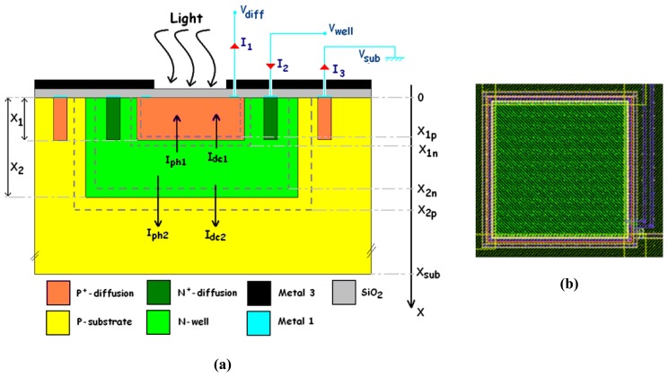
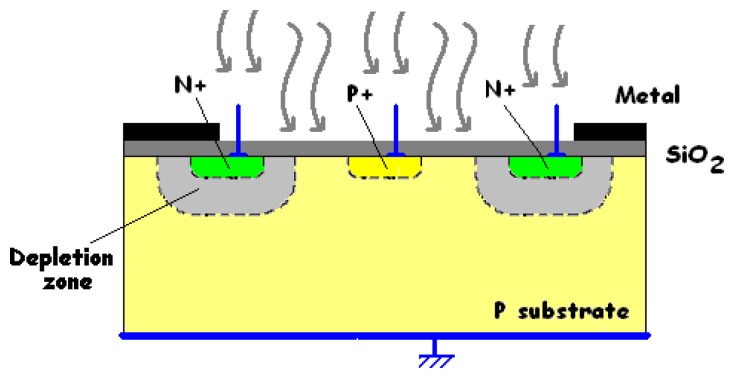
The device consists of two stacked buried photodiodes. Its implementation in a standard n-well CMOS process is illustrated in Figure 1a. It has a vertically stacked shallow P+-diffusion/N-well junction (J1) and a deep P-substrate/N-well junction (J2). The P-substrate is grounded, and two outputs correspond to the P+-diffusion and N-well contacts, respectively. A top metal layer is employed as an optical mask to define the active surface of the detector and to prevent radiation penetration in its peripheral area. The two buried PN junctions (J1 and J2) are reverse-biased, supplying two currents I1 and I2 to the outputs. Observe that the output current I1 flows through the shallow junction, and that the other output current I2 is the sum of the currents passing through both junctions.
Figure 1.
(a) Simplified cross-section of the generic BDJ PD and (b) layout of a square BDJ.
To reverse-bias both junctions, the bias condition is Vwell > Vdiff > Vsub = 0 V, where Vdiff, Vwell and Vsub are the potentials respectively applied to the P+-diffusion, the N-well and the P-substrate (see Figure 1.a).
Under illumination, the current of each junction has two components: a photo-generated component and a dark component. Thus, both output currents can be expressed as:
| (1-a) |
| (1-b) |
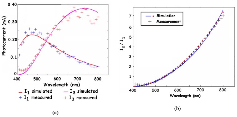
The device operation is based on the strong wavelength dependence of the silicon absorption coefficient α(λ)[3-16, 22, 23, 26, 29-38]. Blue light is absorbed near the silicon surface while red light has a much deeper penetration. Consequently, the shallow junction has a sensitive response to blue light because it collects only photo-generated carriers near the silicon surface. On the other hand, the deep junction is sensitive to red and NIR light thanks to the carriers generated in the deeper region. The spectral responses of both junctions are shown in Figure 2a. Besides, measurements of both output currents allow estimation of the photocurrent ratio I3/I1. This ratio is monotonically increasing with the wavelength, as shown in Figure 2b. Therefore, the BDJ detector can be employed either as a colour- or as a wavelength-sensitive device [3-16, 20].
Figure 2.
Spectral characteristics of a CMOS BDJ detector. (a) Spectral responses of the shallow and deep junctions; (b) photocurrent ratio Iph2/Iph1 versus wavelength.
2.2. Surface reflection
Consider first the bulk silicon surface. Some part of the incident light is reflected. The transmitted part of a photon flux with identical energy can be expressed as:
| (2) |
where R(λ) is the reflection coefficient and Φ(λ) the incident photon flow. R(λ) is given by R = |r|2 where r is the reflection rate calculated from complex Fresnel coefficients [23]. It depends on the air and Si refraction coefficients.
However, a CMOS detector has at least one SiO2 layer on its surface. The reflection index of this surface passivation layer differs from the air and silicon indices. This causes reflections at both the air/SiO2 and SiO2/Si interfaces. Since it is a thin layer, there are interference effects between these reflections, which result in oscillating variations of the effective surface reflection coefficient versus wavelength. Figure 3 shows such variations depending on the SiO2 thickness [3, 10, 27, 28].
Figure 3.
Simulation results of the reflection coefficient R versus wavelength for various SiO2 thickness eox.
The same effects can induce fluctuations on the spectral responses of the detector, as can be observed on the plots of Figure 2a. In the case of CMOS imagers, these reflections may lead to a loss of contrast and sharpness of the obtained images (reflections or “ghosts” on the image). From Equation (2), it can be seen that the reflected light is definitively lost by the detected signal. This leads to a decrease of the quantum efficiency. Solutions for minimizing the reflection effects include anti-reflect coating and a proper choice of the surface layer's thickness.
2.3. Light absorption in silicon and generation rate of electron-hole pairs
When a photon flux with energy hν ≥ EG penetrates inside the silicon bulk, a photoelectric conversion process occurs: ideally, the absorption of one photon creates an electron-hole pair. The generation rate of the electron-hole pairs, at a certain depth from the silicon surface, has the following expression:
| (3) |
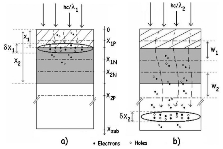
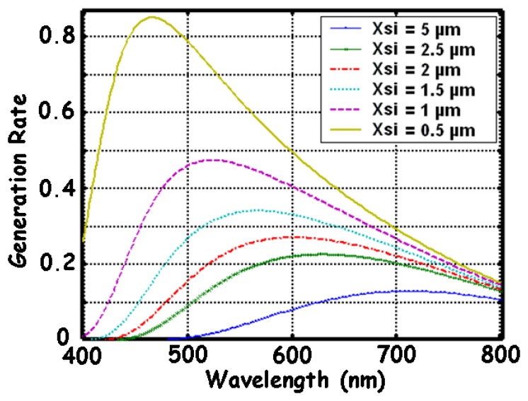
Since it includes the absorption coefficient α, it is dependent of the wavelength. For a given wavelength, the maximum generation rate is proportional to the absorption depth, i.e. × = α-1. This result can mathematically be obtained from Equation (3). It indicates a region depth where most photo-generated carriers are found. For blue light, this depth is about 0.2 μm, and for red light, it is about 5 μm. The region depth of the photo-generated carriers inside a BDJ detector is given as a function of the wavelength in Figure 4. Figure 5 shows the calculated generation rate as a function of the wavelength, for several depths in the silicon.
Figure 4.
Photo-generated carriers inside the BDJ detector in the case of (a) blue light (λ∼450 nm) and (b) red light (λ ∼680 nm).
Figure 5.
Simulation of the normalized generation rate of the electron-hole pairs versus wavelength, for several layers of intrinsic Si.
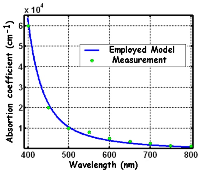
The absorption coefficient in Equation (3) is obviously a key parameter. It strongly depends on the wavelength and on the temperature. There are several analytical or empirical models of the absorption coefficient [29-38], among which the Geist model [29] seems to provide a better agreement with the experimental results at 298 K (see Figure 6). According to this model, the absorption coefficient, expressed in cm-1, can be calculated as:
| (4-a) |
| (4-b) |
The expression (4-a) includes eleven fitted parameters [29], based on [30, 31]: C-11=5030.02 cm-1; C11 = 483.916 cm-1; C-12=1634.30 cm-1; C21 = 79.4079 cm-1; C3=1046.08 cm-1; Ek = 1.09969 eV; E3 = 1.40985 eV; dE1 = 0.0583148 eV; dE2 = 0.0220161 eV; N = 0.394122; dN = 1.23084 eV-1.
Figure 6.
Absorption coefficient of the visible incident light versus wavelength, in silicon, at 298 K.
This equation is an approximation to the theoretical analysis of McLean [30]. The double sum in Equation (4) describes the indirect transition from the parabolic region near the maximum of the valence band to the parabolic region near the minimum of the conduction band. The sum is composed of four terms to describe the emission (j = -1) and the absorption (j = +1) of TO phonons (with energy dE1) and TA phonons (with energy dE2). Finally, the last term in this equation is an attempt to describe the smooth increase beyond the quadratic dependence, as described by McLean. This increase is expected from the increasing density of states in the conduction band due to the deviation of the bands from parabolicity at the higher energies.
To take into account the temperature effect, one may to compute the absorption coefficient by combining this model and experimental data at different temperatures with interpolation techniques [35, 37]. For instance, one may to determine α, by interpolation at any temperature between T1 and T2, is to use the following relationship:
| (5) |
Doping also has an effect on the absorption coefficient. Heavily doped semiconductor may lead to a significant increase of α, due to the band gap narrowing on one hand, and to the absorption contribution of the free carriers on the other hand. However, such an effect may not be noticeable for a doping level lower than 1018 atomes/cm3[38].
2.4. Photocurrents
Under reverse-bias conditions, each junction collects photo-generated charges inside and around its depletion region. The resulting photocurrent across the junction thus has two components: a drift current and a diffusion current [3, 4, 7, 10, 11, 20, 22-24, 26, 40, 43]. The drift component corresponds to charges collected in the depletion layer, and the diffusion current results from charges collected from both quasi-neutral adjacent regions.
The collection process inside the depletion layer of the junction is fast and effective: due to the internal electric field, photo-generated holes and electrons are rapidly separated and flow in opposite directions. Almost all these charges contribute to the photocurrent without being affected by electronhole recombination, which is a much slower process. The drift current can thus be calculated by integrating the generation rate over the depletion layer [3, 4, 7, 10, 11, 19, 20, 22, 24, 26, 40, 43]:
| (6) |
where q is the elementary charge; Aj is the active surface area; θ = 1 or 2 depending on the considered current and W1 and W2 denote the depletion-layer widths.
The diffusion of minority carriers in the quasi-neutral adjacent region toward the depleted region border is a relatively slow process. Due to the recombination, only photo-generated carriers within a diffusion length from the depletion border can be collected and they contribute to the photocurrent. To determine the diffusion currents inside the BDJ detector, the concentration of excess minority carriers should first be calculated by solving the continuity equation with appropriate boundary conditions [3, 4, 7, 10, 11, 19, 20, 24, 26, 40, 43]. Diffusion component can then be determined for any kind of layer by:
| (7-a) |
| (7-b) |
where Dp and Dn represent the diffusion coefficient for holes and electrons respectively; pn and np represent the concentration of excess minority carriers in the observed quasi-neutral region.
Let the minority current through the P+ region be denoted IphD11, while the minority current through the P-substrate will be IphD22. Inside the N-well, two opposite hole diffusion components (IphD12 and IphD21) can be put into evidence. Finally, the following general expression was obtained:
| (8) |
where θ, θ′ = 1 or 2, depending on the considered component; Sθθ′ denotes the diffusion quantum efficiency of the region of interest, which is a function of the geometrical parameters (x1P, W1, etc.), the surface recombination velocity Sr1 (estimated to 107 cm/s, for simulation purposes), the radiation wavelength, the doping profile, etc.
After evaluation of all components, both photocurrents across the shallow and the deep junction can be respectively deduced from the following relationships:
| (9-a) |
| (9-b) |
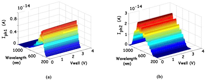
Figure 7 shows an example of the Iph1 and Iph2 computed photocurrents, for a given incident light intensity (1 μW.cm-2). Their variations versus the wavelength represent the spectral responses. The parameters correspond to a 20 μm × 20 μm BDJ detector designed in a 0.35-μm CMOS AMS technology. Since bias voltages are also included in these computations (to determine the depletion-layer depths), the effects of such parameters on the global response can be evaluated. As it appears from Figure 7, the bias voltages have not a strong influence on the photocurrents.
Figure 7.
Matlab computed photocurrents of the BDJ detector versus the wavelength and the reverse bias, considering the reflection coefficient R in SiO2: (a) Photocurrent of the shallow junction J1 and (b) Photocurrent of the deeper junction J2.
In the same way, the temperature dependence of Iph1 and Iph2 can be estimated, provided that the computations include accurate models of the temperature-sensitive parameters such as the absorption coefficient [see Equation (5)], the diffusion coefficient, the carriers' mobility, the intrinsic carrier concentration, etc. In [3], both simulations and measurements show that the peak of Iph1 shifts towards long wavelengths as the temperature increases (a 30 nm variation is estimated between the peaks at 223 K and 338 K) and the spectral response of J1 increases with temperature. For the photocurrent Iph2, the same results were observed.
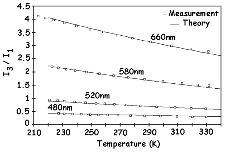
When it operates as a wavelength-sensitive detector, the photocurrent ratio is also an important characteristic of the BDJ sensor. Its temperature-dependence predicted by theoretical computations is confirmed by experimental measurements [3]. Figure 8 depicts an excellent agreement of the results. The photocurrent ratio shows a steady decrease as the temperature increases.
Figure 8.
Photocurrent ratio I3/I1 versus temperature [3].
To compensate temperature effects, it is required to implement some on-chip temperature measurements. One simple solution suggests the use of an N-well resistance as a thermistor [3].
2.5. Response time
In many applications, the response time of the detector to the incident light signal is a benchmark that must be carefully considered and analyzed.
As already mentioned, the photocurrent of a junction has two components: the drift current and the diffusion current. The former has a faster response than the latter, as the charges collecting process differ. Whereas the diffusion current contributes substantially to the overall current (typically in long-wavelength detection), the response time of the detector is primarily set by the diffusion process [3, 21, 25]. Thus, Sedjil et al. [3] studied the impulse response (ideally a Dirac δ(t)) of diffusion currents in quasi-neutral regions, in order to deduce the response to a light pulse (a Heavyside step U(t)). During this very brief moment of illumination, it is assumed that the photo-carriers do neither have time to recombine, nor time to diffuse. Therefore, the density of minority carriers established in each region can lead to the expression of the corresponding diffusion photocurrent component. Since the pulse response is the product of the convolution between the impulse response and a Heavyside step, it can be shown that the time constant of each quasi-neutral region is [3]:
-
▪
which yields τdiff comprised between 0.13 ns and 0.15 ns, with a CMOS 0.8μm technology;(10-a) -
▪
τNwell is in the range [0.14 ns; 0.16 ns];(10-b) -
▪
(10-c)
This corresponds to a time constant τsub between 1 ns and 0.8 μs.
From these equations, we note that the time constants of the quasi-neutral regions depend not only on the lifetimes of the minority carriers (τn1, τn2 and τp) and the minority carrier diffusion constants (Dn1, Dn2 and Dp), but also on the depths of the layer (x1p, x1n, x2n, x2p and xsub). If the thickness of these layers is considered negligible, the lifetime has little influence on the time constant. But for large thicknesses, this time must be taken into account.
An experimental study of the response time of this detector structure has been reported in [25]. With CMOS 1-μm technology and a light wavelength of 783 nm, both rise time and fall time of about 8 ns were observed for the deep junction J2. The surface junction J1 has a shorter response time (about 0.1 ns) because of high doping. These results are typically better than those of a CMOS conventional photodiode, mainly because the BDJ detector has two buried depletion regions instead of one, thus effectively reducing the slow diffusion contribution. In addition to this improvement of the response time, the BDJ detector also has an improved quantum efficiency resulting from its more effective charges collection in silicon.
2.6. Dark currents
Without illumination, the leakage current flowing through a reverse-biased PN junction is called dark current (denoted Idc). This current depends on the junction characteristics and is superimposed to the photocurrent across the junction. It places a limit on the integration duration for measuring the light intensity and it generates a dark noise [19, 20, 46-47]. The value of dark current imposes a physical limit on the two critical benchmarks of any photodetector (PD): the optical detection range and the noise floor.
The particular value of the dark current varies from sample to sample and depends on the temperature, the fabrication quality, the doping level, the bias voltage, the physical design (layout), etc. It is assumed to be mainly due to the thermally generated carriers, but it can be seriously increased due to defects of the semiconductor lattice, dislocations, and unwanted contamination by impurities during fabrication. Furthermore, for image sensors, the dark current may exhibit large variations from pixel to pixel. This dark current non-uniformity increases the Fixed Pattern Noise (FPN) and the Dark Signal Non-Uniformity (DSNU) [19, 20, 48, 49].
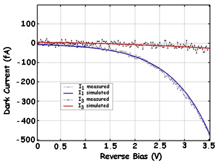
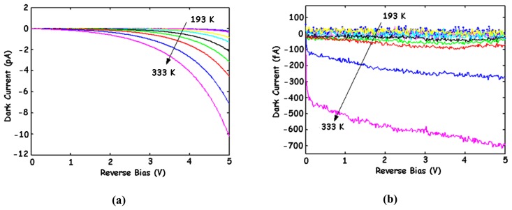
Many physical processes may be involved in the generation of Idc. The most important are the diffusion process, the thermal generation of carriers (Shockley-Read-Hall model), the Band-to-Band Tunnelling (BBT), the Trap-Assisted Tunnelling (TAT) and the impact ionization [17-20, 22, 23, 26, 39, 50-52]. The contributions of these processes depend on the technological and geometrical parameters of the device, the temperature and the bias conditions. The diffusion component may become significant at high temperatures, while the contribution of the thermal generation is related to the depletion-layer width. These two contributions may be identified by their weak dependence on the bias voltage, and their strong dependence on the temperature. In the cases of high-doping and high-bias-voltage conditions, the tunnelling and ionization effects may dominate, which leads to a rapid increase of Idc with the bias voltage. Figure 9 shows the simulated and measured results of both dark currents of a BDJ detector in a 0.35-μm CMOS process. For J1, the dark current exhibits a sensitive increase with the reverse bias voltage, indicating that the diffusion and thermal generation for low voltages (< 1.5 V) and BBT for high voltages (> 1.5 V) are respectively the dominant processes. For J2, the diffusion and thermal generation are the two main contributions, even under a reverse bias up to 3.5 V. The dark current measurements at different temperatures (Figure 10) further confirm this statement [39, 51, 52]. The observed BBT effect on J1 is predictable, because this junction is built with a heavily doped P+-diffusion layer. Finally, both dark currents of the BDJ detector can be expressed as [17-20]:
| (11-a) |
| (11-b) |
where Aj1 and Aj2 are the areas of junctions J1 and J2; Jg1 and Jg2 denote the thermal generation current densities; Jd1 and Jd2 correspond to the diffusion (dark) current densities of J1 and J2; Jt1 is the BBT current density of J1.
Figure 9.
Measured and simulated I–V plots of J1 and J2 junctions in dark, for a 50 × 50 μm2 BDJ at 300 K [17-20].
Figure 10.
Measured dark current of (a) the shallow junction J1 and (b) the deeper junction J2, at various temperatures, for a 50 × 50-μm2 BDJ [51].
To avoid the sharp increase of Idc1 due to the BBT effect, a low reverse bias voltage for J1 is chosen.
3. BDJ SPICE model
The successful design of integrated optical sensor based systems, such as APS for CMOS digital cameras, position sensitive detectors or flame detection, depends on the complete and accurate description of the behaviour of the optical sensor. As simulations are compulsory, an accurate model of the employed photodetector must be found.
A general SPICE model of the BDJ photodetector was proposed for large-, small-signal operations and noise analysis [10, 17-20, 53-55]. An overview is presented in this section, together with its implementation in CAD tools.
3.1. Large-signal, small-signal and noise models
3.1.1. Large-signal model
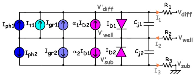
Large-signal operation corresponds to sensor operation either in steady-state or transient state with an intensive incident radiation. The large-signal equivalent circuit is presented in Figure 11, where R1, R2, R3 are parasitic (non-linear) resistances; Cj1, Cj2 denote the junction capacitances; Iph1, Iph2 correspond to the photo-generated currents. The components of Idc1 and Idc2 taken into account are: the thermal G-R components Igr1, Igr2; the BBT current denoted It1. ID1, ID2 stand for the diffusion currents and α1ID2, α2ID1 are the current-controlled current sources performing the mutual coupling between the junctions, like in any Ebers-Moll model of bipolar transistors [17-20, 40, 57].
Figure 11.
Large-signal equivalent circuit of the BDJ PD.
The parasitic resistances correspond to the ohmic contacts and the bulk resistances of the quasi-neutral zones. They reduce the sensor efficiency and slightly modify the junction intrinsic bias (such as , and ). They can be estimated from the sheet and contact resistances (according to the foundry datasheet), from geometrical considerations [57] or by measurement. Thus, for a 20 × 20-μm2 BDJ sensor active area (in the configuration of Figure 1.b), with Vdiff = Vsub = 0 V and Vwell between 0 V and 3.3 V, the worst-case computed parasitic series resistances are around 3 Ω for the P+-diffusion region, 35 Ω for the N-well layer and 7 kΩ for the P-substrate.
Concerning the junction capacitances (Cj1 and Cj2, in Figure 11), as the transition capacitances are negligible under the reverse bias condition, only the non-linear diffusion capacitances are considered. According to [17-20, 26, 58], the junction capacitances can be computed with the following equations:
| (12) |
where the newly introduced parameters are: Pjθ, the perimeter of the considered junction (θ = 1 for J1 and 2 for J2); CjS0θ, the zero-bias junction area capacitance; CjSW0θ, the zero-bias sidewall capacitance; Cj0θ, the zero-bias effective capacitance; Vbiθ, the built-in potential; VbiEFFθ, the effective built-in potential; MjSθ, MjSWθ and Mjθ, dimensionless technological parameters depending on the doping profiles of both PN junctions (with values around 1/2 and 1/3 for the abrupt and the linear junctions respectively); ε0εSi, the silicon permittivity, and .
Note that in the last forms of Equation (12), the area and sidewall contributions are not separated and the capacitance value is estimated with respect to the effective width of the depletion layer [19-20].
3.1.2. Small-signal model
Small-signal operation implies low or variable intensity radiation impinging on the sensor surface. It is usually employed to describe the alternate (dynamic) behaviour of the device due to a perturbation of infinitesimal amplitude, which does not shift the operating point.
As the junction dark and photo-generated currents depend on the optical sensitivities and on the applied bias, the adopted approach consists in taking the exact differential of each DC current equation [17-20]. Obviously, a function depending on the intrinsic junction voltages ( and ) and on the incident optical flow Φt results.
| (13) |
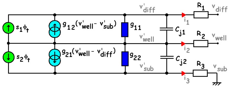
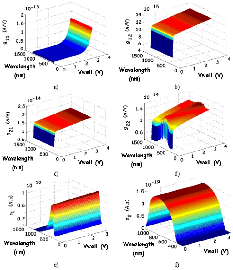
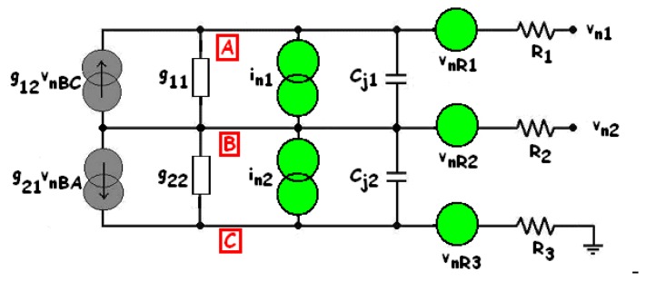
The small-signal equivalent circuit is presented in Figure 12, where, according to Equations (13), the following notation has been adopted: g11 and g22 are the dynamic conductances; g12 and g21 are the transconductances and s1 and s2 are the optical sensitivities (or spectral responses). For a 20 × 20-μm2 sensor in the same conditions as in Figure 7, we find the following maximum values: g11 ≈ 1.4·10-13 S; g22 ≈ 1.5·10-14 S; g12 ≈ 1.4·10-14 A/V and g21 ≈ 2.0·10-14 A/V. As shown in Figures 13.a to 13.d, with an incident red light, the conductance is mainly influenced by the dark and photo-generated G-R current components. Concerning J1, as long as λ is high, the influence of the incident light is not visible and, therefore, only the contribution of the dark current is clearly put in evidence. In contrast, for J2, since Vwell > 0, g22 is monotonically increasing with Vwell and it varies with the radiation wavelength λ consistent with the J2 spectral response. Moreover, for a uniform light as adopted to get the plots of Figure 7, maximum values of 0.5·10-19 A.s.cm2 and 1.49·10-19 A.s.cm2 have been respectively obtained for s1 and s2 (Figures 13.e and 13.f).
Figure 12.
Small-signal equivalent circuit of the BDJ sensor.
Figure 13.
Simulated AC parameters of the BDJ PD (under the same conditions than in Figure 7).
3.1.3. Noise model
The intrinsic electrical noise arises inside the device. It superposes onto the useful signal and tends to obscure its informational content. Considering the various noise mechanisms, the noise equivalent circuit of the BDJ PD (Figure 14) was obtained. It includes three thermal noise voltage generators vnR1, vnR2 and vnR3 to account for the thermal fluctuations arising in the parasitic resistances. It also involves two equivalent current noise generators, denoted In1 and In2, placed at each junction and lumping the effects of the shot, G-R and 1/f noise components. The spectral densities are calculated using the general equations [13, 17-20, 46, 54-56, 59]:
| (14) |
| (15) |
where I corresponds to the DC currents flowing through the considered junction; τT is the relaxation time of the traps; τd denotes the transit mean lifetime of the carriers; f is the frequency of the light radiation; K, σ and κ are device-dependent constants. Typically, we note that 0.5 < σ < 2, 0.8 < κ < 1.3 and K is a constant obtained by fitting experimental data.
Figure 14.
Equivalent noise circuit of the BDJ PD.
3.2. Models implementation in CAD tools
The design of mixed signal systems on chip is nowadays a challenge, especially those including APS for imaging purposes. To simulate such systems, it is necessary to use optoelectronic models of the PDs together with a high level simulator. Conventional circuit simulators, such as SPICE, do not provide models for optoelectronic devices. In order to by-pass this limitation, circuit designers must adopt some tricks that reduce the accuracy. In particular, a simple PN photodiode is normally modelled as a current source, having only a constant capacitance in parallel. In the best case, we have a photocurrent source, modelled from a voltage-controlled current source (where “voltage” is interpreted as the incident power light), in parallel with a diode. However, even if the capacitance and the parasitic resistance of the PD are successfully modelled, the simulation of the photocurrent or dark current behaviours are not satisfactory [18-20, 61-67]. Thus, this simplified approach, although good enough for some applications, is often not suitable to simulate the circuits whose performance is critically dependent on the PD characteristics. To overcome this problem, a rigorous multi-domain approach is generally recommended.
As a first attempt, we have employed SPICE, where a macro-model of PD (using sub-circuits) was proposed to model photocurrents [10-12, 64-67]. After some practice, it appeared clearly that the employment of multi-domains languages, such as Verilog-A and VHDL-AMS, could be very useful. Actually, this approach is the most employed in order to simulate single PD and equally complex Optical System On-Chip (OSOC), having analog and digital parts, with relatively low simulation time [41-44, 68-72]. In this context, the recent availability of the SystemC-AMS language [73, 74] seems to offer the better perspectives for the simulation of complex systems.
Nevertheless, in order to improve the simulation accuracy, various optical sources must also be developed to improve the flexibility of the model implementation in various applications and to allow more realistic simulations. Generally, the optical spectrum is assumed to be white or monochromatic. However, other optical stimuli are possible (light star, incandescent lamps, etc.) and various optical power distributions are possible. For instance, a PD is usually coupled with a LED or a laser, which have a quasi-gaussian spectrum [12, 62, 70, 71].
4. Design and process considerations
This section presents different approaches and considerations to optimize device characteristics, such as noise and dark currents, and spectral responses. Some suggestions point optimal design and proper choice of a given CMOS technology, others require additional process steps. Here, we will mainly focus on the former.
4.1. Solutions to reduce dark currents
Firstly, some efforts are needed to minimize the effects of SiO2/Si interface states. They may generate surface dark current and related shot noise as well as 1/f noise. They may also degrade the blue light response of the detector through surface recombination process. Experimentally, a good rule is to choose P+-diffusion/N-well/P-substrate instead of N+-diffusion/P-well/N-substrate structure, since a high concentration of holes near the silicon surface neutralizes the interface states' effects.
Another rule is to minimize as much as possible the perimeter-to-area ratio. Especially for small-size devices, dark currents are typically dominated by contributions from surface depletion regions [39]. Thus, to minimize side-wall peripheral contribution, instead of adopting BDJs of square-shape, circular or hexagonal shapes are more convenient [75]. Figure 15 shows an example of circular BDJ layout. Circular layout also minimizes BBT effect [76] and junctions capacitances.
Figure 15.
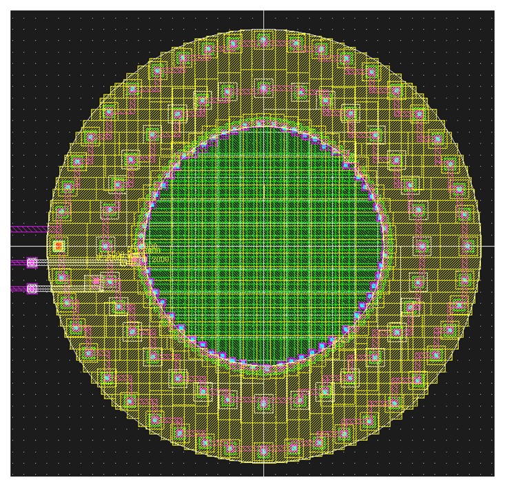
Layout of a circular BDJ PD, where low resistance access, low sidewall component and low crosstalk have been optimized at the expense of the Fill Factor (FF).
Other considerations include effects of some manufacturing steps inducing stress, etching damages etc. For instance, the use of Deuterium annealing instead of the conventional gas annealing process shows good perspectives [77]. Hydrogen annealing was also proved to reduce leakage by passivating the defects [78] In contrast, the use of Shallow Trench Isolation (STI) [79], thin gate oxide, and salicide cause high dark current. To reduce the non-silicided dark current, double-diffused source/drain implantation is used in Active Pixel Sensor (APS) [80].
Aiming at dark current reduction, low bias voltages can be chosen [17-20, 39, 81] and cooling implementation may be considered such as the use of Peltier devices. However, to compensate the temperature effects, some on-chip temperature measurements have to be implemented, by means of thermistors [3].
4.2. Solutions to improve quantum efficiency and Signal-to-Noise Ratio
As it has already been pointed out in Section 2, the spectral response of a buried junction depends on its depth. Consequently, according to the wavelength of interest, the choice of the technology should take into account this aspect. Alternatively, Wolffenbuttel et al. propose to control the spectral sensitivity by modulating the depletion areas (W1 and W2) of both stacked PN junctions [15]. The width of the depletion layers increases with the reverse bias (Vwell-Vdiff and Vwell-Vsub) applied. Hence, their reverse voltages can tune the collecting volumes of both PN junctions. As can be seen from Figure 7, a significant shift of response can be obtained in the region between 360 and 500 nm provided that the width of the depletion layers can vary in the order of 1 μm or more. However, this depletion-width modulation effect can be sensitive only in low doping cases (typically, less than 10-15 cm-3). However, in the most usual submicron CMOS processes, layers with low doping levels are not available.
The most effective optimization is at the process level. Specific implant to control the doping profiles of J1 and J2 may increase quantum efficiency at visible wavelengths and also lower capacitance. Deposition of anti-reflect coating and microlens may improve quantum efficiency. Also, as suggested by Simpson et al. [82], the responsitivity of PDs can also be controlled by using the poly-Si and glass coatings as thin-film optical filters and also by controlling the density of the traps at the interface Si/SiO2. However, these techniques are expensive, requiring specific process optimization and integration.
It is recognized that the use of a shallow junction and a high doping results in a low quantum efficiency. A possible solution, for high visible wavelength, is to use a BiCMOS Buried Triple Junction (BTJ) PD [3-6, 11, 45, 83, 84], where only the middle and the deep junctions are used or, more simply, a P-/N-well/P-sub structure. Moreover, it is admitted that the multi-layer structure increases the quantum efficiency of PDs compared to the simple conventional PN junctions, even for poor quality Si [85-90]. Hence, to increase the quantum efficiency, various SiON materials are being tried out to increase light transmission. Non-silicided deep junctions (such as N-well/P-Sub or N-diff/P-Sub) are generally used [91]. In addition, as it was previously suggested, in connection with our test structures (Figure 1), a metal employed as an optical mask is highly recommended.
Like any photo-sensor, the BDJ detector exhibits several noise sources: shot noise, G-R noise and 1/f noise. It was proved [13, 19, 20] that the Power Spectral Density (PSD) of both the shot and G-R noises increases with the junction current, while, for the 1/f noise, it is a quadratic function of the junction DC current. When the signal level increases, shot (or G-R) noise dominates, but the SNR will still be increased because the photocurrent increases at a faster rate than the noise. At low illumination levels, the 1/f noise may have a significant contribution and all solutions, to reduce it, should be considered. It is well-known that for a zero-voltage bias, the 1/f noise contribution vanishes. However, with zero bias, the PD is rather in the photovoltaic mode, which is not appropriate. Kleinpenning et al. [59] stated that the 1/f noise is proportional to the carriers' lifetime, which, in turn, depends on the doping ( , for an abrupt junction). Thus, the corner frequency, between the shot noise and the flicker noise, decreases with the increasing lifetime. It follows that a lower doping level may help to reduce the 1/f noise. Nevertheless, this possibility is contrary to the actual tendency of continuous downscaling in standard CMOS technologies, where PN junctions at very small depth are made of higher doping layers.
By considering the output signal as the ratio of photocurrents delivered by the BDJ detector, one way to define the SNR is [13]:
| (16) |
Under the assumption that the fluctuations of both photocurrents are uncorrelated, expression (16) shows that this SNR couldn't be higher than those of photocurrents. However, when the noise of the incident light source is dominant, a simultaneous sampling of both output currents is recommended to cancel the common fluctuation part. Consequently, the SNR defined by Equation (16) will be improved.
As far as the deeper junction J2 is concerned, a highly doped epitaxial layer could also be associated with the P-substrate. Thus, the parasitic bulk resistance R3 in Figure 11 will be lowered and the substrate noise will be mitigated. In this way, Wang et al. [91] have implemented their BDJ detector on a high resistivity floating-zone silicon substrate by using ion implantation and this physical structure exhibits low leakage currents.
In order to get better spectral characteristics, some techniques were proposed. To improve the short-wavelength responsivity, some authors [93-95] presented a BDJ detector with a strip-shaped anode geometry (for the shallow junction) to improve UV to green wavelength response. They used interdigitated P+-diffusion fingers to increase the depletion region area near the silicon surface (shown in Figure 16). The idea is similar to that of a lateral photodiode [43], to improve the collecting efficiency of photo-generated carriers near silicon surface. Another valuable idea to obtain a wide spectrum responsitivity was suggested by Pinna [85]. He proposed a structure consisting of two phototransistors, one vertical, the other lateral (see Figure 17). In reference [96], Yang et al. present a method for improving the spectral sensitivity of PDs manufactured in commercial 0.18-μm silicon CMOS technology, without the addition of post-processed colour filters. Similarly to microwaves techniques, combining the BDJ detector and metallic grids on its surface (Figure 18) enhances the sensitivity by an additional control of the spectral sensitivity and by shifting the region of high sensitivity to longer wavelengths. Note that Findlater et al. [97-99] designed a CMOS colour image sensor based on two BDJ detector pixels with deposited colour filters. In this way, four different spectral responses were obtained, which enabled tri-chromatic colour detection.
Figure 16.
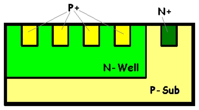
Simplified cross-section of the UV/Blue improved BDJ PD [93-95].
Figure 17.
Simplified cross-section of the large-band light sensor proposed by A. Pinna [85].
Figure 18.
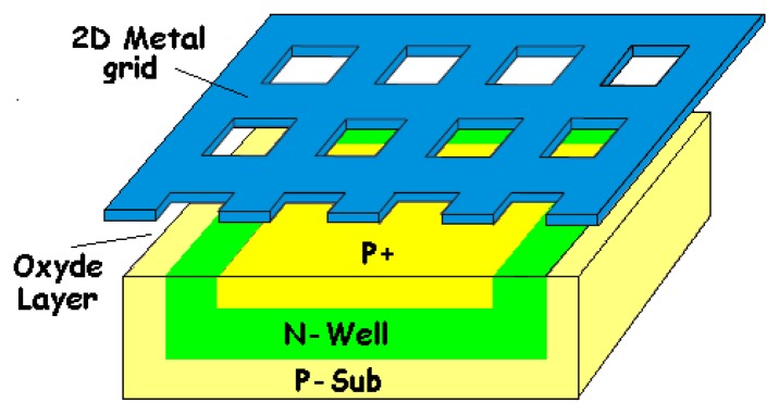
Associating the BDJ PD with a two-dimensional (2-D) metal grid [96].
In practice, various detector sizes are required by specific applications. High-resolution imaging devices call for small-size implementation. In standard CMOS technology, the P+-diffusion layer is surrounded by N-well. Due to peripheral spacing rules imposed by the technology, the Fill Factor (FF) will deteriorate rapidly when the pixel pitch is limited to a few micrometers. However, it is possible (with advanced technologies) to bury thin oppositely-doped layers at different depths for collecting photocarriers [101]. The deep buried layer will not envelop the shallow one and in this way avoids peripheral spacing limitation and thus allows further reduction of pixel size. On the other hand, when very large size detectors are required, another limitation is set by the condition that the bulk substrate potential must not vary along the structure. In practice, for the bias of high-resistivity layers (such as N-well and P-substrate), multi-point contacts between each 100 μm or so should be provided to maintain equipotentiality. As bias contacts for P-substrate and N-well cannot be made in the central area of the detector, a possible solution for a large-size detector is to design an array of parallel-connected pixels.
5. Examples of applications in integrated CMOS optical sensors
This section presents examples of BDJ-based integrated systems especially for imaging applications. Such developments primarily exploit the spectral characteristics of the BDJ detector and its double operations enabling intensity and wavelength detection.
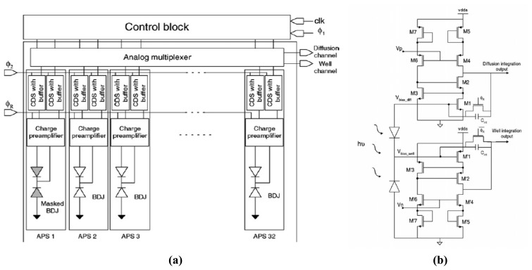
One example, shown in Figure 19, is a CMOS APS linear array [102, 103], dedicated to be a self-wavelength calibration micro-spectrophotometer. Each pixel integrates a BDJ detector both for light intensity measurement (like a photodiode) and for wavelength estimation of the received monochromatic component. The 32-active pixels linear array is designed to meet high-sensitivity and low-resolution requirements. The in-pixel electronic circuit includes a two-channel charge preamplifier and correlated-double-sampling (CDS) stages, as shown in Figure 19.
Figure 19.
(a) Block diagram of the CMOS APS linear array and (b) schematic of one pixel with its two-channel charge preamplifier [102].
The BDJ detector has also gained interest in many 2D imaging systems [3, 4, 20, 53-55, 78, 97-99, 104, 105]. In a project developing colour image sensors, Findlater et al. [98-100] employed two BDJ-based pixels instead of 3 or 4 conventional PD-based pixels for tri-chromatic colour detection. The idea of this example is to exploit the integrated colour filtering properties of the BDJ detector. We can see from Figure 2a that the shallow junction has a selective response for blue light, while the deep junction exhibits a high sensitive response for red and NIR light. Combining such spectral responses with colour filter deposition on top of the two pixels, one may measure the colour by applying a trichromatic method. This approach, compared to 3 or 4-pixel colour imaging, presents several improvements in spatial frequency, resolution and colour accuracy. In [106-108], De Graaf et al. proposed a microsystem for illumination source identification.
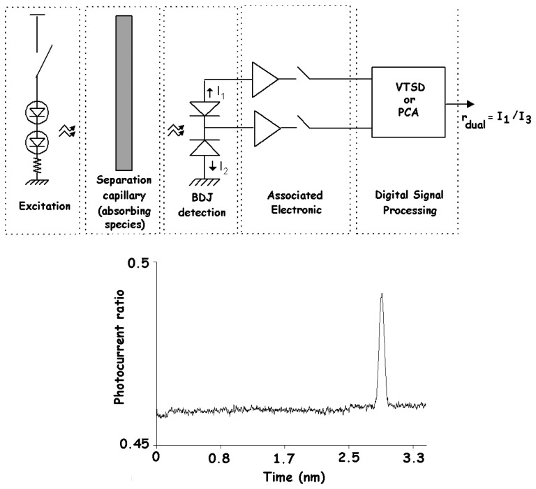
One important feature of the traditional BDJ detector lies in the photocurrent ratio evaluation by measuring its two outputs. Considering the spectral sensitivities plotted in Figures 2a and 2b and remembering that the surface reflection (see Section 2.2) may induce fluctuations on the spectral responses but has no effect on the photocurrent ratio, this may be a key issue in some particular applications. More generally, the fluctuations of the incident light intensity will not affect the photocurrent ratio, provided that both detector outputs are synchronously red [9, 13]. On the other hand, the photocurrent ratio can be exploited both to estimate the wavelength in the case of a monochromatic light source and to detect the spectral variations for the non-monochromatic excitation. This led to the developments of specific optical methods for detecting spectral changes without any dependence on the intensity variations. Figure 20 shows a dual-wavelength method recommended for a quantitative analysis via absorptiometric measurements [110-112].
Figure 20.
Capillary absorptiometric measurement with dual-wavelength method [110].
The operation of the BDJ detector is particularly attractive to implement the optical detection for biochemical analysis. Taking fluorescence detection as an example, its photodiode mode can serve to quantify the species by measuring the fluorescence intensity, while its wavelength-detection mode allows spectral discrimination in the multi-label cases or detected signal estimation [112].
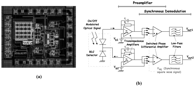
To implement the micro-channel and micro-capillary detection, Figure 21 presents a chip integrating a 4 × 4-array of BDJ pixels. It enables either individual pixel reading or parallel connections of all the pixels operated as a single BDJ detector. For such applications, a large-area detector for the micro-channel adaptation of the optical-fiber-coupling is typically employed and the custom design of associated electronics is suggested to improve the SNR. The custom design allows the on-chip implementation of some noise reduction techniques, such as charge/transimpedance preamplifier, a synchronous detection (see Figure 21b) [110, 112] or high-gain differential approaches [116]. The chip of Figure 21a was used for capillary fluorescence detection. The evaluated limit of detection was below 10-10 M in fluorescein isothiocyanate (FITC) concentration for a small volume of 5 nL [114].
Figure 21.
(a) Chip integrating an array of 4 × 4 BDJ pixels: (b) on-chip charge / transimpedance preamplifier and synchronous detection [112, 113].
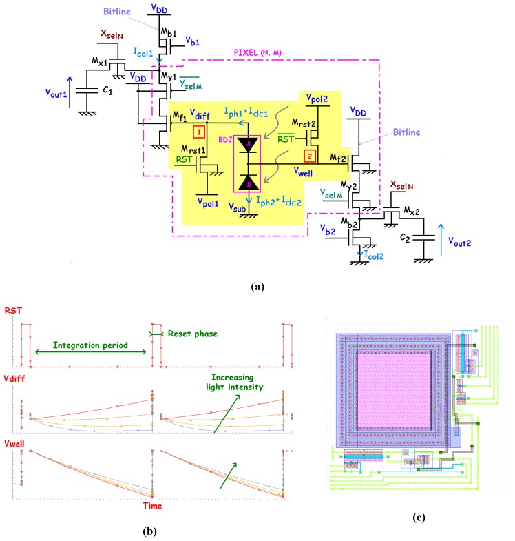
For 2D imaging applications requiring a good spatial resolution, the APS solution is an obvious choice. Many studies on in-pixel BDJ-associated electronics were reported [20, 53-55, 97-99]. Figure 22 shows an active pixel with simultaneous reset, integration and read operations for both channels. This architecture makes use of 6-transistors pixel. Thanks to its synchronous operations for both channels, the obtained photocurrent ratio will not be affected by the temporal fluctuations of the incident light intensity. This architecture can also be improved. For instance, a better FF may be obtained by sharing the same readout circuit between two neighbour pixels. Two shutters (i.e., MOSFETs) can be introduced between the BDJ outputs and the source follower transistors to isolate photo-generated signals (before or after reset transistors [117]). Moreover, according to [104-105], BDJ could be employed in 3D image reconstruction, where the first junction J1 provides the visible response and the second J2 the IR response.
Figure 22.
(a) CMOS BDJ APS architecture, (b) its corresponding timing diagram obtained from simulation and (c) its layout.
6. Conclusions
In this paper, the state of the art of the BDJ optical sensor has been presented. It puts in evidence that this sensor, realized in standard CMOS technology, presents a real interest for low-cost and low-power applications. Since the BDJ provides two responses in a single pixel, this detector presents a better performance than any conventional photodiode. It is obvious that the BDJ photodetector can find a wide range of applications, such as micro-instrumentation (biomedical, chemistry, drug detection, etc.), communication systems, image sensors and more.
References and Notes
- 1.Fossum E.R. Proc. SPIE. Vol. 2172. San Jose, CA, USA: Feb 6-10, 1994. Active Pixel Sensor: Are CCDs Dinosaurs? pp. 2–14. [Google Scholar]
- 2.Meynants G., Dierickx B., Scheffer D. Proc. SPIE. Vol. 3410. San Diego, CA, USA: Jul 19, 1998. CMOS Active Pixel Image Sensor with CCD Performance; pp. 68–76. [Google Scholar]
- 3.Sedjil M. Modélisation de Capteurs de Couleur Intégré et Développement d'Application; Thesis. Vol. 7. University D. Diderot; Paris: 1999. [Google Scholar]
- 4.Ben Chouikha M. Développement de Détecteurs de Couleur dans des Technologies Standards de CI (CMOS et BiCMOS): Application à la Réalisation de Capteurs Intégrés pour l'Imagerie Electronique et l'Instrumentation; Thesis. Vol. 7. University D. Diderot; Paris: 1999. [Google Scholar]
- 5.Ben Chouikha M., Lu G.N., Sedjil M., Sou G. A Photodetector Based on Buried Junctions and Corresponding Method of Manufacture. US Patent. No 08/816383. 1996
- 6.Ben Chouikha M., Viénot F. Proc. IS&T/SPIE. Vol. 9. San Jose, CA, January: 1999. Colorimetric Characterisation of Color Detector, Implanted in a BiCMOS Technology; pp. 105–110. [Google Scholar]
- 7.Sedjil M., Lu G.N., Ben Chouikha M., Alexandre A. Proc. SPIE. Vol. 3680. Denver, CO, USA: Jul 18, 1999. Modeling of BDJ and BTJ Structures for Color Detection; pp. 388–397. [Google Scholar]
- 8.Lu G.N., Ben Chouikha M., Sou G., Sedjil M. Color Detection Using a Buried Double p-n Junction Implanted in the CMOS Process. Electron. Lett. 1996;35:594–596. [Google Scholar]
- 9.Lu G.N., Ben Chouikha M., Sedjil M., Sou G., Alquie G. Investigation of the Buried Double p-n Junction Implanted in CMOS Technology for Wavelength-Sensitive Detection. Int. J. Electron. 1997;83:307–316. [Google Scholar]
- 10.Alexandre A., Ben Chouikha M., Sedjil M., Alquie G. Proc. MSM. San Diego, CA; 2000. An improved BDJ Photodetector Physical Model under Spice; pp. 189–192. Ch. 5. [Google Scholar]
- 11.Alexandre A., Lu G.N., Chea A., Sedjil M., Ben Chouikha M. C2I, Instrumentation, Interdisciplinarité et Innovation. Colloque interdisciplinaire en instrumentation; Paris, France: Nov, 1998. Modèles Spice de Deux Nouveaux Capteurs Optiques Intégrés (BDJ et BTJ) pour le Développement de Microsystèmes; pp. 403–410. [Google Scholar]
- 12.Alexandre A., Sou G., Ben Chouikha M., Sedjil M., Lu G.N., Alquie G. Proc. SPIE. Vol. 4019. San Diego, CA, USA: Jul 30, 2000. Modeling and Design of Multi Buried Junctions Detectors for Color Systems Development; pp. 288–298. [Google Scholar]
- 13.Lu G.N., Sou G., Devigny F., Guillaud G. Design and Testing of a CMOS BDJ Detector for Integrated Micro-Analysis. Microelectronics. 2001;32:227–234. [Google Scholar]
- 14.Ben Chouikha M., Lu G.N., Sedjil M., Sou G. Proc. SPIE. Vol. 3410. San Diego, CA, USA: Jul 19, 1998. A CMOS Linear Array of BDJ Color Detector; pp. 46–53. [Google Scholar]
- 15.Wolffenbuttel R.F. Silicon Photodetectors with a Selective Spectral Response. In: Baltes H., Hesse J., Korvink J., editors. Sensors Update. Vol. 9. Wiley; New York: 2001. pp. 69–101. [Google Scholar]
- 16.Middelhoek S., Audet S.A. Silicon Sensors. Academic Press; New York: 1989. [Google Scholar]
- 17.Feruglio S., Haned F., Vasilescu G., Ben Chouikha M., Sou G., Fouad Hanna V., Alquie G. Proc. IEEE IST. Lyon, France; Jun, 2004. A General Model of the CMOS Buried Double Junction Photodetector; pp. 60–65. [Google Scholar]
- 18.Feruglio S., Vasilescu G., Alquie G., Fouad Hanna V. Modelling of the CMOS Buried Double Junction Photodetector. Microw. Opt. Techn. Lett. 2005;45:507–514. [Google Scholar]
- 19.Feruglio S., Fouad Hanna V., Alquie G., Vasilescu G. Dark Current and Signal-to-Noise Ratio in BDJ Image Sensors. IEEE Trans. Instrum. Meas. 2006;55:1892–1903. [Google Scholar]
- 20.Feruglio S. Etude du Bruit dans les Capteurs d'Images Intégrés, type APS; Thesis. Vol. 6. University Pierre & Marie Curie; Paris: 2005. [Google Scholar]
- 21.Dillon P.L., Brault A.T., Horak J.R., Garcia E., Martin T.W., Light W.A. Fabrication and Performance of Colour Filter Arrays for Solid-State Imagers. IEEE Trans. Electron. Dev. 1978;25:97–101. [Google Scholar]
- 22.Mathieu H. Physique des semi-conducteurs et des composants électroniques. Ed. Masson; Paris: 1998. [Google Scholar]
- 23.Toffano Z. Optoélectronique, Composants photoniques et fibres optiques. Ed. Ellipses: Paris; 2001. [Google Scholar]
- 24.Lee J.S., Hornsey R.I. Photoresponse of Photodiode Arrays for Solid-State Image Sensor. J. Vaccum. Sci. Technol. 2000;18:621–625. [Google Scholar]
- 25.Lalanne P., Rodier J.-C. CMOS Photodiode Based on Vertical p-n-p Junctions. Proc. WOCS. 1997. http://ipdps.cc.gatech.edu/1997/wocs/lalanne.pdf.
- 26.Sze S.M. Physics of Semiconductor Devices. 2ND ed. J. Wiley & Sons; New York: 1981. [Google Scholar]
- 27.Alexandre A., Ben Chouikha M., Alquie G. OHD Conf. Besançon, France: Sep, 1999. Identification de l'épaisseur de l'oxyde de silicium et des longueurs de diffusion dans les différentes couches d'un capteur optique intégré silicium. [Google Scholar]
- 28.Huen T. Reflectance of Thinly Oxidized Silicon at Normal Incidence. Appl. Optics. 1979;18:1927–1931. doi: 10.1364/AO.18.001927. [DOI] [PubMed] [Google Scholar]
- 29.Geist J., Migdall A., Baites H.-P. Analytic Representation of the Silicon Absorption Coefficient in the Indirect Transition Region. Appl. Optics. 1988;27:3777–3779. doi: 10.1364/AO.27.003777. [DOI] [PubMed] [Google Scholar]
- 30.McLean T.P. The Absorption Edge Spectrum of Semiconductors. Prog. Semiconductors. 1960;5:53. [Google Scholar]
- 31.Rajkanan K., Singh R., Shewchun J. Absorption Coefficient of Silicon for Solar Cell Calculations. Solid-State Electron. 1979;22:793–795. [Google Scholar]
- 32.Dash W.C., Newman R. Intrinsic Optical Absorption in Single-Crystal Germanium and Silicon at 77K and 300K. Phys. Rev. 1955;99:1151–1155. [Google Scholar]
- 33.Philipp H.R., Taft E.A. Optical Constant of Silicon in the Region 1 to 10 eV. Phys. Rev. 1960;120:37–38. [Google Scholar]
- 34.Kuhl C., Schlotterer H., Schwidefsky F. Optical Investigation of Different Silicon Film. J. Electrochem. Soc.: Solid-State Sci. Tech. 1974;121 No. 11. [Google Scholar]
- 35.Varshni Y.P. Temperature Dependence of the Energy Gap in Semiconductors. Physica. 1967;34:149. [Google Scholar]
- 36.Rajkanan M., Singh R., Schewchun J. Absorption Coefficient of Silicon for Solar Cell Calculations. Solid-State Electron. 1979;22:793–795. [Google Scholar]
- 37.Dash W.C., Newman R. Intrinsic Optical Absorption in Single-Crystal Germanium and Silicon at 77°K and 300°K. Phys. Rev. 1955;99:1151–1155. [Google Scholar]
- 38.Schmid P.E. Optical Absorption in Heavily Doped Silicon. J. Am. Phys. Soc. 1981;23:5531–5536. [Google Scholar]
- 39.Loukianova N.V., Folkerts H.O., Maas J.P, Verbugt D.W.E., Mierop A.J., Hoekstra W., Roks E., Theuwissen A.J.P. Leakage Current Modelling of Test Structure for Characterization of Dark Current in CMOS Image Sensor. IEEE Trans. Electron. Dev. 2003;50:77–83. [Google Scholar]
- 40.Alexandre A., Pinna A., Granado B., Garda P. DCIS. Bordeaux, France: Nov, 2004. Modeling and simulation of phototransistors using VHDL-AMS. [Google Scholar]
- 41.Dadouche F., Alexandre A., Pinna A., Granado B., Garda P. FDL Conf. Lille, France: Sep, 2004. A VHDL-AMS Configuration for Active Pixel Sensors. [Google Scholar]
- 42.Dadouche F., Pinna A., Garda P., Alexandre A. Proc. IEEE DTIS. Tunisia: Sep 5-7, 2006. Modeling of Pixel Sensors for Image Systems with VHDL-AMS; pp. 289–293. [Google Scholar]
- 43.Alexandre A., Dadouche F., Garda P. Proc. IEEE DTIS. Tunisia: Sep 5-7, 2006. Two Dimensional Model for Lateral Photodiode; pp. 294–298. [Google Scholar]
- 44.Dadouche F., Pinna A., Garda P., Alexandre A. Modeling of Pixel Sensors for Image Systems with VHDL-AMS. Int. J. Electron. 2008;95:211–225. [Google Scholar]
- 45.Ben Chouikha M., Vienot F., Lu G.N. Proc. SPIE. Vol. 3410. Denver, CO, USA: Jul 18, 1999. Temperature Effect on Colorimetric Accuracy of the BTJ Color Detector; pp. 204–214. [Google Scholar]
- 46.Vasilescu G. Electronic Noise and Interfering Signals: Principles and Applications. Springer-Verlag; Heidelberg, Germany: 2005. [Google Scholar]
- 47.Vandamme L.K.J. Noise as a Diagnostic Tool for Quality and Reliability of Electronic Devices. IEEE Trans. Electron. Dev. 1994;41:2176–2187. [Google Scholar]
- 48.El Gamal A., Fowler B., Min H., Liu X. Proc. SPIE. Vol. 3301. San Diego, CA, USA: Jul 19, 1998. Modeling and Estimation of FPN Components in CMOS Image Sensors; pp. 168–177. [Google Scholar]
- 49.Johansson R. Implementation of an Active Pixel Sensor with Shutter and Analog Summing in a 0.35 μm Process. Thesis. University of Linköping; 2003. [Google Scholar]
- 50.Haned F., Ben Chouikha M., Alquie G. MOS Modeling and Parameter Extraction Workshop. Strasbourg, France: Apr, 2005. An Improved BDJ Color Detector Physical Model. [Google Scholar]
- 51.Haned F., Ben Chouikha M., Alquie G. Proc. IEEE MIXDES Conf. Gdynia, Poland: Jun, 2006. Temperature Effect on the Buried Double Junction Color Detector Behavior; pp. 107–110. [Google Scholar]
- 52.Haned F., Ben Chouikha M., Alquie G. ICNMT Conf. Tizi-Ouzou, Algeria: Nov, 2006. I-V Characterization for a Deeper Comprehension of Buried Double Junction Color Detector Behavior. [Google Scholar]
- 53.Feruglio S., Garda P., Vasilescu G. Noise Characterization of a CMOS Two-colour APS. MOC Tech. Dig. 2005:114–115. [Google Scholar]
- 54.Feruglio S., Fouad Hanna V., Alquie G., Vasilescu G. Proc. SPIE. Vol. 5846. San Jose, CA, USA: Feb 27, 2005. Temporal Signal-to-Noise Ratio of a CMOS Buried Double Junction Image Sensor; pp. 180–191. [Google Scholar]
- 55.Feruglio S., Fouad Hanna V., Alquie G., Vasilescu G. Proc. IEEE ISCAS. Vol. 3. Kobe, Japan; May, 2005. Exact Noise Analysis of a CMOS BDJ APS; pp. 2337–2340. [Google Scholar]
- 56.Feruglio S., Pinna A., Chay C., Llopis O., Granado B., Alexandre A., Garda P., Vasilescu G. Proc. WSEAS CSCC. Athens, Greece: 2006. Noise Characterization of CMOS Image Sensors; pp. 102–107. [Google Scholar]
- 57.Laker K.R., Sansen W.M.C. Design of Analog Integrated Circuits and Systems. McGraw-Hill; New York: 1994. [Google Scholar]
- 58.Aharoni H., Ohmi T. Analysis of n+p Silicon Junctions with Varying Substrate Doping Concentrations Made Under Ultra Clean Processing Technology. J. Appl. Phys. 1997;81:1270–1288. [Google Scholar]
- 59.Kleinpenning T.G.M. 1/f Noise in p-n Junction Diodes. J. Vacuum Sci. Technol. A. 1985;3:176–182. [Google Scholar]
- 60.Feruglio S., Pinna A., Llopis O., Chay C., Granado B., Alexandre A., Garda P., Vasilescu G. Noise Characterization in a CMOS 0.6-μm PPS Image Sensors System. WSEAS Trans. Circ. Syst. 2006;5:877–886. [Google Scholar]
- 61.Ravezzi L., Dalla Betta G.-F., Stoppa D., Simon A. A Versatile Photodiode SPICE Model for Optical Microsystem Simulation. Microelectr. J. 2000;31:277–282. [Google Scholar]
- 62.Alexandre A., Sou G., Ben Chouikha M., Sedjil M., Lu G.N., Alquie G. Proc. SPIE. Vol. 4019. San Diego, CA, USA: Jul 30, 2000. Modeling and Design of Multi Buried Junctions Detectors for Color Systems Development; pp. 288–298. [Google Scholar]
- 63.Alexandre A., Sedjil M., Ben Chouikha M., Alquie G. Proc. SPIE. Vol. 4408. San Diego, CA, USA: Jul 29, 2001. Modeling and Simulation Under SPICE of Optoelectronic Systems Including BDJ Detector; pp. 138–146. [Google Scholar]
- 64.Neifeld M.A., Chou W.-C. SPICE-Based Optoelectronic System Simulation. Appl. Optics. 1998;37:6093–6104. doi: 10.1364/ao.37.006093. [DOI] [PubMed] [Google Scholar]
- 65.Desai N.R., Hoang K.V., Sonek G.J. Applications of PSPICE Simulation Software to the Study of Optoelectronic Integrated Circuits and Devices. IEEE Trans. Edu. 1993;36:357–362. [Google Scholar]
- 66.http://www.spectrum-soft.com/news/summer2004/photodiode.shtm
- 67.http://www.orcad.com/documents/community.an/pspice/tn27.aspx
- 68.Haned F., Ben Chouikha M., Baguennier-Desormaux A., Alquie G. MOS Modeling and Parameter Extraction Workshop. Leuven, Belgium: Sep, 2004. Verilog-A Behavioral Models of Optoelectronic Devices for Color Sensor Design. [Google Scholar]
- 69.Haned F., Ben Chouikha M., Baguennier-Desormaux A., Alquie G. Proc. SPIE. Vol. 5677. San Jose, CA, USA: Feb 27, 2005. Optoelectronic Library for color Sensor Design; pp. 16–25. [Google Scholar]
- 70.Haned F., Ben Chouikha M., Baguennier-Desormaux A., Alquie G. MIXDES Conf. Krakow, Poland: Jun, 2005. An Improved BDJ Verilog-AMS Model Implemented in Cadence Virtuoso Plateform for Color Sensor Design. [Google Scholar]
- 71.Haned F., Ben Chouikha M., Baguennier-Desormaux A., Alquie G. READ Conf. Evry, France: Jun, 2005. Développement d'une Bibliothèque de Composants Optoélectroniques pour le Simulateur Spectre. [Google Scholar]
- 72.Haned F., Ben Chouikha M., Baguennier-Desormaux A., Alquie G. CDNLive EMEA Conf. Nice, France: Jun, 2006. Optoelectronic Library Implemented under Cadence Virtuoso Platform for Color Sensor Design. [Google Scholar]
- 73.Vachoux A., Grimm C., Einwich K. Proc. IEEE ISCAS. Vol. 3. Bangkok, Thailand: May 25-28, 2003. Analog and Mixed Signal Modelling with SystemC-AMS; pp. 914–917. [Google Scholar]
- 74.Alassir M., Denoulet J., Romain O., Suissa A., Garda P. Modelling Field Bus Communications in Mixed-Signal Embedded Systems. EURASIP J. Emb. Syst. 2008;2008:733–744. [Google Scholar]
- 75.http://www.dpreview.com/news/0301/03012202fujisuperccdsr.asp
- 76.Tournier A., Roy F., Lu G.-N., Deschamps B. 1.4μm-Pitch, 50%-fill-factor, 1T Charge-Modulation Pixel for CMOS image sensors. IEEE Electron. Dev. Lett. 2008;29:221–223. [Google Scholar]
- 77.Kwon H.I., Kwon O.J., Shin H., Park B.-G., Park S.S., Lee J.D. The Effects of Deuterium Annealing on the Reduction of Dark Currents in the CMOS APS. IEEE Trans. Electron. Dev. 2004;51:1346–1349. [Google Scholar]
- 78.Wuu S.G., Chien H.C., Yaung D.N., Tseng C.H., Wang C.S., Chang C.K., Hsiao Y.K. A High Performance Active Pixel Sensor with 0.18-μm CMOS Color Imager Technology. IEEE IEDM Tech. Dig. 2001:555–558. [Google Scholar]
- 79.Han S.-W., Yoon E. Low Dark Current CMOS Image Sensor Pixel with Photodiode Structure Enclosed by P-well. Electron. Lett. 2006;42:1145–1146. [Google Scholar]
- 80.Merrill R.B. CMOS Image Sensor Employing Silicide Exclusion Mask to Reduce Leakage and Improve Performance. US Pat. 6160282. 2000
- 81.Carrillo G., Lu G.N., Pittet P., Zhao K. Proc. IEEE ICECS. Nice, France: Dec 10-13, 2006. CMOS BDJ Detector Array with Charge Preamplifiers for Sensitive Biochemical Analysis; pp. 367–370. [Google Scholar]
- 82.Simpson M.L., Ericson N.N., Jellinson G.E., Jr., Dress W.B., Wintenberg A.L., Bobrek M. Application Specific Spectral Response with CMOS Compatible Photodiodes. IEEE Trans. Electron. Dev. 1999;46:905–913. [Google Scholar]
- 83.Gilblom D.L., Yoo S.K., Ventura P. Proc. SPIE. Vol. 5074. San Jose, CA, USA: Feb 15-20, 2003. Operation and Performance of a Color Image Sensor with Layered Photodiodes; pp. 318–331. [Google Scholar]
- 84.Billings Merrill R., Brehmer K. Color Separation in an Active Pixel Cell Imaging Array Using a Triple-Well Structure. US Pat.5965875. 1999
- 85.Pinna A. Conception d'une Rétine Connexionniste: du Capteur au Système de Vision sur Puce. Thesis. Vol. 6. University Pierre & Marie Curie; Paris: 2003. [Google Scholar]
- 86.Green M.A. Collection Probability Equals Dark Minority Carrier Concentration and Other Surprising Solar Cell Relations. IEEE Photovoltaic Specialists Conf; New York, USA. Sep 29 - Oct 3, 1997; pp. 211–214. [Google Scholar]
- 87.Green M.A., Zhai J., Zheng G.F. Eur. Photovolt. Solar Ener.Conf. Exhib. Barcelona, Spain: Jun, 1997. High Efficiency Crystalline Silicon Multilayer Solar Cells. [Google Scholar]
- 88.Brecl K., Furlan J. Proc. Eur. Photovolt. Solar Ener. Conf. Vol. 2. Glasgow, UK: May, 2000. Modelling Floating Junction Solar Cells; pp. 1293–1297. [Google Scholar]
- 89.Brecl J., Furlan K. MSM Conf. San Diego, California, USA; Mar 27-29, 2000. Modelling Multilayer Semiconductor Structures; pp. 376–379. [Google Scholar]
- 90.Dierickx B., Bogaerts J. Proc. SPIE. Vol. 5301. Denver, CO, USA: Aug 1, 2004. NIR-Enhanced Image Sensor Using Multiple Epitaxial Layer; pp. 205–212. [Google Scholar]
- 91.El Gamal A. Proc. IEEE IEDM. San Francisco: Dec 8-11, 2002. Trends in CMOS Image Sensor Technology and Design; pp. 805–808. [Google Scholar]
- 92.Wang W.J., Liu X.L., Li W., Ren H.R., Liang K., Han D.J. A Blue-Violet Enhanced BDJ Photodetector and its Applications in the Probe Chip Measurements of the LEDs for Solid-State Lighting. Sens. Actuat. A. 2007;136:168–172. [Google Scholar]
- 93.Pauchard A., Besse P.-A., Popovic R.S. A Silicon Blue UV Selective Stripe-Shaped Photodiode. Sens. Actuat. A. 1999;76:172–177. [Google Scholar]
- 94.Pauchard A., Furrer B., Randjelovic Z., Rochas A., Manic D., Popovic R.S. Integrated Microsystem for Blue/UV Detection. Sens. Actuat. B. 2000;85:99–105. [Google Scholar]
- 95.Yotter R.A., Warren M.R., Wilson D.M. Optimized CMOS Photodetector Structures for the Detection of Green Luminescent Probes in Biological Applications. Sens. Actuat. B. 2000;103:43–49. [Google Scholar]
- 96.Yang F., Titus A.H. Integrated Colour Detectors in 0.18-μm CMOS Technology. Electron. Lett. 2007;43:1279–1281. [Google Scholar]
- 97.Findlater K.M. A CMOS Camera Employing a Double Junction Active Pixel. Thesis. University of Edinburgh; 2001. [Google Scholar]
- 98.Findlater K.M., Denyer P.B., Hurwitz J.E.D., Raynor J.M., Renshaw D. Proc. IEEE CCDs & AIS. Santa Clara, CA: Jun 28-29, 1999. Buried Double Junction Pixel Using Green and Magenta Filters; pp. 60–64. [Google Scholar]
- 99.Findlater K.M., Renshaw D., Hurwitz J.E.D., Henderson R.K., Bailey T.E.R., Smith S.G., Purcell M.D., Raynor J.M. Proc. IEEE CCDs & AIS. Lake Tahoe, California: Jun 7-9, 2001. A CMOS Image Sensor Employing a Double Junction Photodiode; pp. 60–63. [Google Scholar]
- 100.Malhotra V. Method of using DC Photocurrent Measurements to Sense Wavelength or Color of Light or to Characterize Semiconductor Materials. US Pat. 5270536. 1993
- 101.Hynecek J., Merrill R.B., Martin R.A. Method and apparatus for improving sensitivity in vertical color CMOS image sensors. US Pat. Appl. 20050194653. 2005
- 102.De Graaf G., Riedijk F.R., Wolffenbuttel R.F. Colour-Sensor System with Frequency Output and an ISS or I2C Bus Interface. Sens. Actuat. A. 1997;61:441–445. [Google Scholar]
- 103.De Graaf G., Wolffenbuttel R.F. Smart Optical Sensor Systems in CMOS for Measuring Light Intensity and Colour. Sens. Actuat. A. 1998;67:115–119. [Google Scholar]
- 104.De Graaf G., Wolffenbuttel R.F. Illumination Source Identification Using a CMOS Optical Microsystem. IEEE Trans. Instrum. Meas. 2004;53:238–242. [Google Scholar]
- 105.De Graaf G., Wolffenbuttel R.F. Optical CMOS Sensor for Detection of Light Sources. Sens. Actuat. A. 2004;10:77–81. [Google Scholar]
- 106.Kolar A., Graba T., Pinna A., Romain O., Granado B., Ea T. Proc. IEEE ICECS. Vol. 10. Nice, France: Dec 10-13, 2006. An Integrated Digital Architecture for Real-Time Reconstruction in VSIP Sensor, Electronics, Circuits and Systems; pp. 144–147. [Google Scholar]
- 107.Kolar A., Graba T., Pinna A., Romain O., Granado B., Belhaire E. DCIS Conf. Sevilla, Spain: Nov 2007, A Multi Shutter Time Sensor for Multispectral Imaging in a Reconstruction Embedded Sensor. [Google Scholar]
- 108.Sedjil M., Lu G.N. A Seawater pH Determination Method Using BDJ Detector. Meas. Sci. Technol. 1998;9:1587–1592. [Google Scholar]
- 109.Lu G.N. A Dual-Wavelength Method Using the BDJ Detector and its Application to Iron Concentration Measurement. Meas. Sci. Technol. 1999;10:312–315. [Google Scholar]
- 110.Pittet P., Lu G. N., Bertoncini N., Renaud L. CMOS Absorbance Detection System for Capillary Electrophoresis. Mater. Sci. Eng. C. 2006;26:282–289. [Google Scholar]
- 111.Lu G.N. A Dual-Wavelength Method Using the BDJ Detector and its Application to Iron Concentration Measurement. Meas. Sci. Technol. 1999;10:312–315. [Google Scholar]
- 112.Lu G.N., Pittet P., Sou G., Carrillo G., El Mourabit A. Proc. IEEE ICECS. Croatia, Yugoslavia: Sep 15-18, 2002. On-Chip Synchronous Detection for CMOS Detection; pp. 355–358. [Google Scholar]
- 113.Lu G.N., Pittet P., Sou G., Carrillo G., El Mourabit A. A Novel Approach to Implementing On-Chip Synchronous Detection for CMOS Optical Detector Systems. Analog Integr. Circ. S. 2003;37:57–66. [Google Scholar]
- 114.Pittet P., Galvan J.-M., Lu G.N., Blum L.J., Leca-Bouvier B.D. CMOS LIF Detection System for Capillary Analysis. Sens. Actuat. B. 2003;97:355–361. [Google Scholar]
- 115.Pittet P., Lu G. N., El Mourabit A. Proc. IEEE ICECS. Croatia, Yugoslavia: Sep 15-18, 2002. On-Chip Transimpedance Preamplifier for CMOS BDJ Optical Detector Using Active Enhanced Impedance Loads; pp. 351–354. [Google Scholar]
- 116.Xu W., Mathine D.L., Barton J.K. High-Gain Differential CMOS Transimpedance Amplifier with On-Chip buried Double Junction Photodiode. Electron. Lett. 2006;42:803–805. [Google Scholar]
- 117.Wäny M., Israel G.P. CMOS Image Sensor with NMOS-Only Global Shutter and Enhanced Responsivity. IEEE Trans. Electron. Dev. 2003;50:57–62. [Google Scholar]


