Abstract
The quest for a solid state universal memory with high-storage density, high read/write speed, random access and non-volatility has triggered intense research into new materials and novel device architectures. Though the non-volatile memory market is dominated by flash memory now, it has very low operation speed with ~10 μs programming and ~10 ms erasing time. Furthermore, it can only withstand ~105 rewriting cycles, which prevents it from becoming the universal memory. Here we demonstrate that the significant photovoltaic effect of a ferroelectric material, such as BiFeO3 with a band gap in the visible range, can be used to sense the polarization direction non-destructively in a ferroelectric memory. A prototype 16-cell memory based on the cross-bar architecture has been prepared and tested, demonstrating the feasibility of this technique.
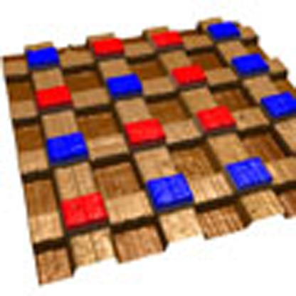 Ferroelectric RAM is considered a promising candidate on the quest for a universal memory, but the concept is still problem prone. Here, the authors use the ferroelectric photovoltaic effect as a non-destructive read-out method for a new prototype memory, which shows good data retention and fatigue resistance.
There are several contenders being actively explored by the industry for the universal memory. These include resistive switching random access memory based on filamentary conduction and/or interface barrier modulation by defects1,2, phase change memory3,4 and magnetic random access memory, which uses tunnelling magnetoresistance effect5,6. Though they operate at higher speed than flash memory7, all of them have high-energy consumption, which is detrimental for portable applications, besides other drawbacks.
A ferroelectric random access memory (FeRAM) stores information using the spontaneous polarization of ferroelectric materials. An external voltage pulse can switch the polarization between two stable directions, representing ‘0’ and ‘1’. It is non-volatile and the read/write process can be completed within nanoseconds. However, despite its great promise, FeRAM has a negligible share of today’s memory market, mainly due to process integration and cost issues. One problem associated with conventional FeRAM is that reading is performed by applying a bias to the ferroelectric capacitor and detecting the polarization-switching current. This process is destructive and a rewrite step is needed. Furthermore, it also requires a minimum capacitor size to generate enough current for the sensing circuit. To realize the full potential of FeRAM, it is highly desirable to have a non-destructive read-out method. Recently, the resistance change of a ferroelectric tunnel junction upon polarization reversal has been demonstrated and it can be used to sense the polarization direction non-destructively8,9,10. However, this approach requires the ferroelectric layer to be several nanometres thick at most, which poses a tremendous challenge on the device fabrication.
The photovoltaic effect has been observed in ferroelectrics several decades ago11. Indeed, early work had even proposed the use of the photovoltaic effect for information transfer and storage applications12,13. Although the maximum open circuit voltage (Voc) is typically limited by the band gap of the material, in some cases, anomalously large values of Voc have been reported. Recently, it was proposed that energy band bending at domain walls may be the origin of above band gap Voc (ref. 14). In a ferroelectric single crystal or epitaxial film, a combination of residual depolarization field and interface depletion layers can explain the polarization-dependent photovoltaic effect15. BiFeO3, a multiferroic material with robust ferroelectric and magnetic order at room temperature16, and a band gap (~2.7 eV) that is within visible light range17, offers a unique opportunity for memory application. As both signs of Voc and short circuit photocurrent (Isc) depend on the polarization direction18,19,20, they can serve as the read-out signal in a memory device.
We have investigated the photovoltaic effect of single-domain BiFeO3 films. Both Voc and Isc can be reversed by voltage pulses as short as 10 ns, indicating high writing speed of the memory. The data retention, fatigue performance and energy consumption of the device compare favourably with other technologies under development. A prototype memory using the cross-bar architecture has been prepared and tested. The results clearly demonstrate the feasibility of this concept.
Results
Device preparation and characterizations
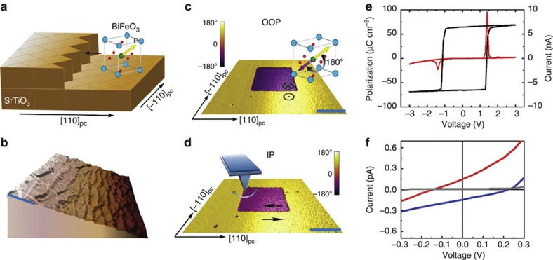
Epitaxial BiFeO3 films of 100 nm are grown using pulsed laser deposition (PLD) on (001) SrTiO3 single-crystal substrates. We use La0.7Sr0.3MnO3 as the bottom electrode (see Methods for details). Basic properties of the films are summarized in Supplementary Figure S1. To eliminate complications from multiple domains in BiFeO3, we have used miscut substrates (4° towards (110)) to obtain single-domain films as illustrated in Fig. 1a–d. The BiFeO3/La0.7Sr0.3MnO3 interface at the step edge lifts the degeneracy of the multiple domains in BiFeO3, and the preferred polarization direction is indicated. Following the BiFeO3 deposition, an array of 5-μm × 5-μm Fe electrodes (5 nm thick) are patterned on top for subsequent electrical and photovoltaic characterizations (Supplementary Fig. S2a). Five nanometer Pt is deposited on top of Fe to prevent oxidation. Fe is chosen as the top electrode based on our investigation on the polarization fatigue in BiFeO3. We have learned that charge injection at the electrode/BiFeO3 interface leads to domain pinning. When the pinned domains grow across the film, macroscopic fatigue occurs21. Furthermore, our recent study has revealed that the Schottky barrier at the interface is critical for the charge injection process. By using a low work function metal to reduce the barrier height, charge injection can be greatly reduced and fatigue performance significantly improved22. The transmission coefficient of the Pt/Fe layer is about 35% within the visible spectrum (Supplementary Fig. S3).
Figure 1. Properties of as-grown BiFeO3 thin films.
(a) Schematic drawing of BiFeO3 unit cell on SrTiO3 substrate with 4° miscut towards (110) direction. The interface between the bottom electrode and BiFeO3 at the step edge favors one of the eight degenerate polarization directions. (b) Topography of the BiFeO3 film with steps that are clearly visible and obtained by atomic force microscopy (AFM). (c) Out-of-plane (OOP) and (d) in-plane (IP) domain images of the BiFeO3 film. A 2-μm × 2-μm square region with opposite polarization direction was created by scanning the area with a DC bias applied to the AFM tip. (e) Typical P–V hysteresis loop (black) obtained at room temperature using 1 kHz triangle wave. The I–V curve (red) is also shown. (f) Current–voltage curves of the as-grown film obtained with and without illumination (grey line: in dark; red line: under light with polarization down; blue line: under light with polarization up. Light source: halogen lamp; energy density: 20 mW cm−2). Scale bars, 1 μm.
The ferroelectric polarization–voltage (P–V) hysteresis loop shown in Fig. 1e (measured at 1 kHz. See Supplementary Fig. S4 for frequency-dependent P–V loops) reveals a remnant polarization of ~65 μC cm−1 along the [001]pc (the subscript pc refers to pseudo cubic) direction, consistent with earlier reports and indicative of the high quality of the films16,23. The coercive voltage is about 1.3 V, which can be further reduced by decreasing the film thickness or by chemical substitution in BiFeO3. The applied voltage is termed as positive (negative) if a positive (negative) bias is applied to the top electrode. After poling the polarization up (down) by applying a voltage pulse of −3 V (+3 V), the I–V curves demonstrate clear photovoltaic effect under light (light source: halogen lamp; energy density: 20 mW cm−2, which is 1/5 of one sun intensity). As shown in Fig. 1f, the Voc is 0.21 V and Isc is −0.15 pA for the polarization up state, and −0.13 V/0.15 pA for the polarization down state. It is thus possible to determine the polarization direction (stored information) by sensing the photovoltage or photocurrent, and this process is non-destructive. The switchable nature of the photovoltaic effect implies that it is related to the spontaneous polarization of BiFeO3. This has been discussed in detail in the literature18,19,20. Basically, due to incomplete compensation of the polarization charges, the residual depolarization field is always in the opposite direction of the polarization. The depolarization field drives the photo-generated electrons and holes into opposite direction before they recombine. The asymmetric Voc and Isc under positive and negative polarization directions is likely due to the different work functions of the top and bottom electrodes, which also induces an internal field that does not depend on the polarization direction.
Photovoltaic behaviour
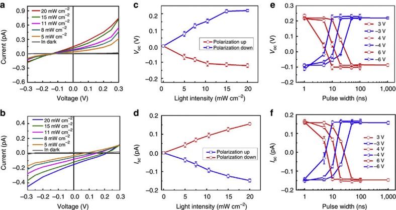
As expected, the photovoltaic response of the device depends on the intensity of the light. When the light intensity increases, both Voc and Isc increase (Fig. 2a–d). Although the Voc saturates at ~0.21 and –0.13 V, no saturation is observed for Isc up to 20 mV cm−2. Increasing light intensity can generate more electron-hole pairs which are separated by the internal field and lead to larger Voc and Isc. To assess the operation speed of the memory cells, we measure the influence of the poling pulse width on the photovoltaic response and the results are shown in Fig. 2e. Square pulses of 1 ns to 1 ms are used to control the polarization direction of the film, and the I–V curves under 20 mW cm−2 light were measured subsequently. When 6 V pulses are applied, the spontaneous polarization starts to switch within several nanoseconds. At 10 ns, the polarization is fully reversed and both Voc and Isc reach expected values. This result demonstrates that the memory cell can be written within 10 ns. However, this is by no means the limit. In fact, polarization switching by pulses of <1 ns has been reported in the literature, with the ultimate limit being set by the acoustic phonon mode (velocity of sound) in the material24. For the reading process, as it does not require switching of polarization and the light can be kept on whenever the device is in operation, so the photovoltaic response of every cell is always ready for reading and the speed is only limited by the RC-time constant of the circuit. What’s even more attractive is that, if we use Voc as the sensing signal, the memory cell can be as small as lithography technique allows, as Voc does not depend on the lateral size of the capacitor.
Figure 2. Photovoltaic effect of the Fe/BiFeO3/La0.7Sr0.3MnO3/SrTiO3 device.
Current-voltage curves measured under different light intensity for (a) polarization down and (b) up states. (c) Voc and (d) Isc as functions of light intensity for both polarization directions. Pulse width dependences of (e) Voc and (f) Isc measured with different pulse heights.
Retention and fatigue
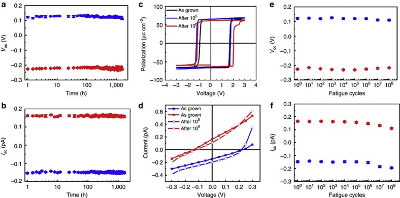
For non-volatile memory application, long data retention and superior fatigue resistance are two critical requirements. We have monitored the Voc and Isc of several memory cells for 4 months, no deterioration in the signal has been observed (Fig. 3a). Furthermore, the memory cells have been subjected to bipolar switching for up to 108 cycles and show no sign of fatigue (Fig. 3c–f). It is also well known in the ferroelectric community that fatigue can be mitigated by using oxide electrodes, suggesting that the non-volatile memory can sustain much more read/write cycles than flash memory.
Figure 3. Retention and fatigue behavior of the memory cell.
(a) Voc and (b) Isc for both polarization directions show negligible change after 4 months. (c) P–V loops and (d) current-voltage curves measured after repetitive switching by pulses of ±3 V, 1 ms reveal no fatigue after 108 cycles. In (a,b,d–f), blue: under light with polarization up; red: under light with polarization down.
Prototype device characterization
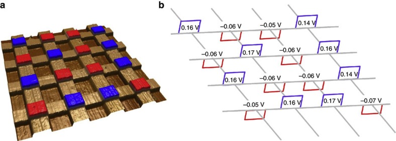
To assess the scalability of the photovoltaic effect-based FeRAM, we have prepared and tested a prototype memory using the cross-bar architecture. The bottom La0.7Sr0.3MnO3 film is patterned through photolithography process and etched into stripes of 2,000 μm × 10 μm. After deposition of the BiFeO3 film, top Pt/Fe electrodes of the same size are prepared (see Methods for details). The measurement setup is schematically shown in Supplementary Fig. S2b. Figure 4a depicts the topographic image of the device and each junction represents a memory cell. Despite the large size of each cell, limited by our lithography facility, all of them are fully functional. After poling the polarization direction in each cell randomly, we obtain the Voc under 20 mW cm−2 light by measuring the I–V curve of each cell. The results are shown in Fig. 4b. The absolute values are slightly different from those obtained from the single capacitors. But the results clearly demonstrate the feasibility of this concept. Typical memory performance, that is, data retention and fatigue, has been tested for the cross-bar device. The results are similar to that of the single capacitors (Supplementary Fig. S5).
Figure 4. Performance of a prototype 16-cell memory based on the cross-bar architecture.
(a) Topography of the device with preset polarization direction. Blue: polarization up, red: polarization down. (b) Voc of all 16 cells are indicated. These are measured under 20 mW cm−2 light.
A fundamental problem for the cross-bar architecture is that sneak paths may form, which bypass the target memory cell being addressed. Practically, this can be prevented by integrating a transistor with each cell even though it reduces the memory density. In fact, the 1 transistor 1 capacitor structure is employed in conventional ferroelectric memory. However, in the proposed device, each cell generates Voc and Isc under light by itself. No external driving force is needed during the reading process. The sneak path problem is rather different from that in the memresistive cross-bar memory. Further study is underway to clarify this issue.
Discussion
It is noteworthy that the results reported here are obtained from typical BiFeO3 capacitors as proof of concept. Further optimization on the film thickness and electrode materials selection could improve the Voc and the Isc for better performance. For example, using electrodes with larger screening length should enhance Voc due to increasing depolarization field. Furthermore, the concept is not limited to BiFeO3. Other ferroelectric materials, for example, PZT and BaTiO3, should give rise to similar behaviour. Compared with flash memory, the photovoltaic FeRAM reported here has much higher operation speed and lower energy consumption. It also compares favourably with other non-volatile memories that are under development currently, for example, magnetic random access memory and resistive switching random access memory (see Supplementary Table S1). In summary, we report here a novel approach to create a non-volatile memory technology that uses the polarization-dependent photovoltaic effect in ferroelectrics.
Methods
Device preparation
PLD technique was used to prepare the La0.7Sr0.3MnO3 bottom electrode and epitaxial BiFeO3 films. High-energy KrF excimer laser (λ=248 nm) was used. La0.7Sr0.3MnO3 of 20 nm was deposited at 670 °C with the oxygen partial pressure of 300 mTorr. The laser energy density and repetition rate were 1 J·cm−2 and 3 Hz, respectively. Following the deposition of the bottom electrode, epitaxial BiFeO3 film was grown using a Bi0.8FeO3 target with substrate temperature of 680 °C and oxygen partial pressure of 50 mTorr. The laser energy density and repetition rate were 1 J·cm−2 and 10 Hz, respectively. After the deposition of BiFeO3, photolithography was conducted to prepare the 5-μm × 5-μm top electrodes. The sample surface was first coated with a buffer layer of LOR 5 A (Microchem) using spin coater at 4,000 r.p.m., followed by baking at 110 °C for 2 min. After this, a layer of positive photoresist EPG 510 (Everlight) was coated at 4,000 r.p.m. and baked at 110 °C for 2 min. The sample was then attached to a photomask for UV light (350 W) exposure for 6 s using LithoPack 300 (SUSS MicroTec). The desired patterns were obtained by developing in TMAH (Kanto) solution for 18 s to remove the exposed photoresist. After the photolithography, Pt (5 nm)/Fe (5 nm) electrodes were deposited by PLD. The remaining photoresist was removed by a remover solution (MicroChem).
For the cross-bar device, photoresist in the shape of 2,000 μm × 10 μm stripes were created on the bottom La0.7Sr0.3MnO3 film through photolithography. The rest of the La0.7Sr0.3MnO3 film was etched away in a KI/HCl (1:9) solution. The remaining photoresist was removed by remover. After this, the SrTiO3 substrate with La0.7Sr0.3MnO3 electrodes was cleaned by acetone and ethanol, followed by BiFeO3 deposition. The top Pt/Fe electrodes are of the same size as the bottom La0.7Sr0.3MnO3 electrodes but in the perpendicular direction. So a capacitor of 10 μm × 10 μm is formed at each junction.
Electrical characterizations
Piezoresponse force microscopy measurement was carried out on a commercial atomic force microscope (Asylum Research MFP-3D) using Pt/Ir-coated tip. I–V curves were measured using a pA metre/direct current (DC) voltage source (Hewlett Package 4140B) on a low noise probe station. The light source was a Halogen lamp and the illumination energy density used in this study ranged from 5 to 20 mW cm−2. Ferroelectric properties and switching experiments were carried out using a commercial ferroelectric tester (Radiant Technologies, Inc.) and a pulse generator (Keithley 3401).
Author contributions
J.W. conceived and designed the experiments. R.G. prepared the films and devices. R.G., L.Y., Y.Z., Z.S.L. and X.Z. conducted the electrical and photovoltaic characterizations. R.G., L.C., R.R. and J.W. wrote the paper. All the authors discussed the results and commented on the manuscript.
Additional information
How to cite this article: Guo, R. et al. Non-volatile memory based on the ferroelectric photovoltaic effect. Nat. Commun. 4:1990 doi: 10.1038/ncomms2990 (2013).
Supplementary Material
Supplementary Figures S1-S5 and Supplementary Table S1
Acknowledgments
This work is supported by National Research Foundation of Singapore under project NRF-CRP5-2009-04. R.R. acknowledges partial support from the NSF E3S Center.
References
- Yang J. J. et al. Memristive switching mechanism for metal/oxide/metal nanodevices. Nat. Nanotech. 3, 429–433 (2008). [DOI] [PubMed] [Google Scholar]
- Waser R. & Aono M. Nanoionics-based resistive switching memories. Nat. Mater. 6, 833–840 (2007). [DOI] [PubMed] [Google Scholar]
- Wuttig M. & Yamada N. Phase-change materials for rewriteable data storage. Nat. Mater. 6, 824–832 (2007). [DOI] [PubMed] [Google Scholar]
- Kolobov A. V. et al. Understanding the phase-change mechanism of rewritable optical media. Nat. Mater. 3, 703–708 (2004). [DOI] [PubMed] [Google Scholar]
- Chappert C. Fert A. & Van Dau F. N. The emergence of spin electronics in data storage. Nat. Mater. 6, 813–823 (2007). [DOI] [PubMed] [Google Scholar]
- Åkerman J. Toward a universal memory. Science 308, 508–510 (2005). [DOI] [PubMed] [Google Scholar]
- Shim S. I. Yeh F. C. Wang X. W. & Ma T. P. SONOS-type flash memory cell with metal/Al2O3/SiN/Si3N4/Si structure for low-voltage high-speed program/erase operation. IEEE Elec. Dev. Lett. 29, 512–514 (2008). [Google Scholar]
- Chanthbouala A. et al. Solid-state memories based on ferroelectric tunnel junctions. Nat. Nanotech. 7, 101–104 (2011). [DOI] [PubMed] [Google Scholar]
- Garcia V. et al. Giant tunnel electroresistance for non-destructive readout of ferroelectric states. Nature 460, 81–84 (2009). [DOI] [PubMed] [Google Scholar]
- Gajek M. et al. Tunnel junctions with multiferroic barriers. Nat. Mater. 6, 296–302 (2007). [DOI] [PubMed] [Google Scholar]
- Brody P. & Crowne F. Mechanism for the high voltage photovoltaic effect in ceramic ferroelectrics. J. Electron. Mater. 4, 955–971 (1975). [Google Scholar]
- Brody P. Ferroelectric photovoltaic method and apparatus for transferring information. US Patent US4103341 (1978).
- Thakoor A. P. & Thakoor S. Thin film ferroelectric electro-optic memory. US Patent US005206829A (1993).
- Yang S. Y. et al. Above-bandgap voltages from ferroelectric photovoltaic devices. Nat. Nanotech. 5, 143–147 (2010). [DOI] [PubMed] [Google Scholar]
- Yuan G. L. & Wang J. L. Evidences for the depletion region induced by the polarization of ferroelectric semiconductors. Appl. Phys. Lett. 95, 252904 (2009). [Google Scholar]
- Wang J. et al. Epitaxial BiFeO3 multiferroic thin film heterostructures. Science 299, 1719–1722 (2003). [DOI] [PubMed] [Google Scholar]
- Ihlefeld J. F. et al. Optical band gap of BiFeO3 grown by molecular-beam epitaxy. Appl. Phys. Lett. 92, 142908–142903 (2008). [Google Scholar]
- Choi T. Lee S. Choi Y. J. Kiryukhin V. & Cheong S. W. Switchable ferroelectric diode and photovoltaic effect in BiFeO3. Science 324, 63–66 (2009). [DOI] [PubMed] [Google Scholar]
- Ji W. Yao K. & Liang Y. C. Bulk photovoltaic effect at visible wavelength in epitaxial ferroelectric BiFeO3 thin films. Adv. Mater. 22, 1763–1766 (2010). [DOI] [PubMed] [Google Scholar]
- Yi H. T. Choi T. Choi S. G. Oh Y. S. & Cheong S. W. Mechanism of the switchable photovoltaic effect in ferroelectric BiFeO3. Adv. Mater. 23, 3403–3407 (2011). [DOI] [PubMed] [Google Scholar]
- Zou X. et al. Mechanism of Polarization Fatigue in BiFeO3. ACS Nano 6, 8997–9004 (2012). [DOI] [PubMed] [Google Scholar]
- Zhou Y. et al. Mechanism of polarization fatigue in BiFeO3: the role of Schottky barrier. Preprint at http://arxiv.org/abs/1304.7935 (2013).
- Baek S. H. et al. Ferroelastic switching for nanoscale non-volatile magnetoelectric devices. Nat. Mater. 9, 309–314 (2010). [DOI] [PubMed] [Google Scholar]
- Li J. et al. Ultrafast polarization switching in thin-film ferroelectrics. Appl. Phys. Lett. 84, 1174–1176 (2004). [Google Scholar]
Associated Data
This section collects any data citations, data availability statements, or supplementary materials included in this article.
Supplementary Materials
Supplementary Figures S1-S5 and Supplementary Table S1


