Main Text
Localized surface plasmon resonance (LSPR), owing to collective oscillation of conduction-band electrons in noble-metal (Au, Ag) nanostructures, induces greatly enhanced electric (E) fields in confined nanoscale locations, such as on the tips of nanorods or in the junctions of nanodimers.[1] These locations are called hot spots. In the vicinity of hot spots, Raman scattering spectra of biochemicals can be substantially amplified with E4 dependence due to E-field enhancement of both the incident light and Raman scattering spectra.[1c] This phenomenon is called Surface Enhanced Raman Scattering (SERS)[2] and has drawn intensive research interest due to the potential applications in label-free and multiplex biochemical detection.[3] The effect of SERS is so pronounced that the enhancement factor (EF) can reach 1010 at the junctions of Ag nanoparticles,[4] where single-molecule events can be readily observed.[1c, 4a, 5] However, the practical applications of SERS for ultrasensitive biochemical detection is still challenging because (1) it is difficult to create a large number of hotspots with controlled junctions at a low cost for sensitive and relatively reproducible detection[6]. (2) It is even more arduous to flexibly assemble the hotspots at desirable positions for location predicable sensing.
Previous research in biochemical detection with SERS spectroscopy utilized aggregates of colloidal plasmonic nanoparticles, where the hotspots are random in dimensions, quantity, and location by nature.[7] The recent breakthrough of On-Wire Lithography (OWL)[8] has made it possible to control the gap sizes of metallic nanodisk/rod pairs to a few nanometers and has demonstrated single-molecule sensitivity for various biochemicals such as methylene blue,[1d] p-mercaptoaniline,[9] and Cy-3-labeled DNA.[10] However, the OWL applications are still limited by the low density of hot spots. Other methods including E-beam lithography,[11] nanosphere/colloidal lithography[12], and porous template assisted deposition[13] were explored for sensitive and location-predictable SERS sensing. However, creating a large number of strong hotspots remains challenging due to the difficulty in controlling the gap size to only a few nanometers. Recently, an elegant concept for manufacturing self-assembled nanofingers has been explored to tackle the aforementioned problems. Li et al. have successfully created ordered arrays of gold-capped-polymer nanofingers in a large area by nanoimprint lithography.[14] Controlled numbers of nanofingers can be readily snapped together by surface tension from solvent evaporation where hotspots were created in the junctions with an EF of ~ 1011.[14a] [14b] However, nanoimprint lithography requires elaborate instruments and once the mask pattern is made, the arrangement of hotspots cannot be easily altered. Based on a similar concept, Schmidt et al. economically created hotspots in assembled silver-capped Si nanopillars via maskless reactive ion etching. At the most closely packed configuration of the nanopillars, a hotspot density of 30/µm2 and an EF 2.1×10¹¹ were achieved. However, the positions of the hotspots cannot be precisely controlled due to the irregular positioning of nanopillars.[15]
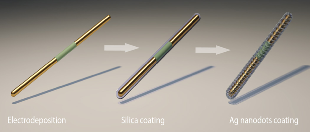
In this work, we tackle the aforementioned problems by economically synthesizing SERS nanocapsules and flexibly assembling them into designed arrays with electric fields for ultrasensitive and location-predictable biochemical sensing. A plasmonic nanocapsule consists of a tri-layer structure with a three-segment Ag/Ni/Ag nanorod as the core, a thin layer of silica as the capsulating layer, and uniformly distributed Ag NPs on silica as the hotspot layer (Scheme 1). Each layer in these nanocapsules serves a specific purpose. The inner metallic nanorod cores can be electrically polarized and thus manipulated by electric tweezers[16] based on combined AC and DC electric fields and the embedded Ni magnets in the nanorods assist the assembly of the nanocapsules onto patterned nanomagnets at designated locations; the central silica layer provides a supporting substrate for the synthesis of the Ag NP arrays, which also effectively separates the plasmonic Ag NPs from the metallic nanorod cores to eliminate plasmonic quenching; finally, the outermost layer made of Ag NPs with optimized sizes and junctions provides a large number of hot spots (~1200/µm2) for ultrasensitive detection. We have transported and assembled such nanocapsules into ordered arrays using our recent nano-manipulation invention, the “electric tweezers”. A prototype of 3×3 nanocapsule sensor array has demonstrated of the ability to successfully detect various biochemicals. Such Raman nanosensors are designed and fabricated to remove obstacles that hinder the applications of SERS and may inspire new designs of Raman nanosensors.
Scheme 1.
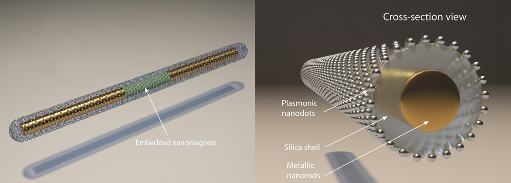
Structure of a tri-layer nanocapsule.
The fabrication of nanocapsules follows the steps in Scheme 2: we started with the synthesis of multisegment Ag/Ni/Ag nanorods (300 nm in diameter, LAg= 2.5 µm, LNi= 1 µm) by electrodeposition in nanoporous anodized aluminum oxide membranes that have been described previously.[8c, 8d] In brief, a Cu layer of 500 nm in thickness was sputtered onto the back of the membrane to seal the pores and also serve as the working electrode in a three-electrode electrodeposition system. The electrodeposition of the nanowires from the working electrode commenced at the bottom of the nanopores. The amount of electric charge passing through the circuit controls the length of the segments of the Ag/Ni/Ag nanowires in the membrane. After dissolving the membrane in 2 M NaOH solution, the nanowires were washed by sonication and centrifuging in ethanol and deionized (D.I.) water twice before resuspended in D.I.water.
Scheme 2.
Synthesis process of nanocapsules.
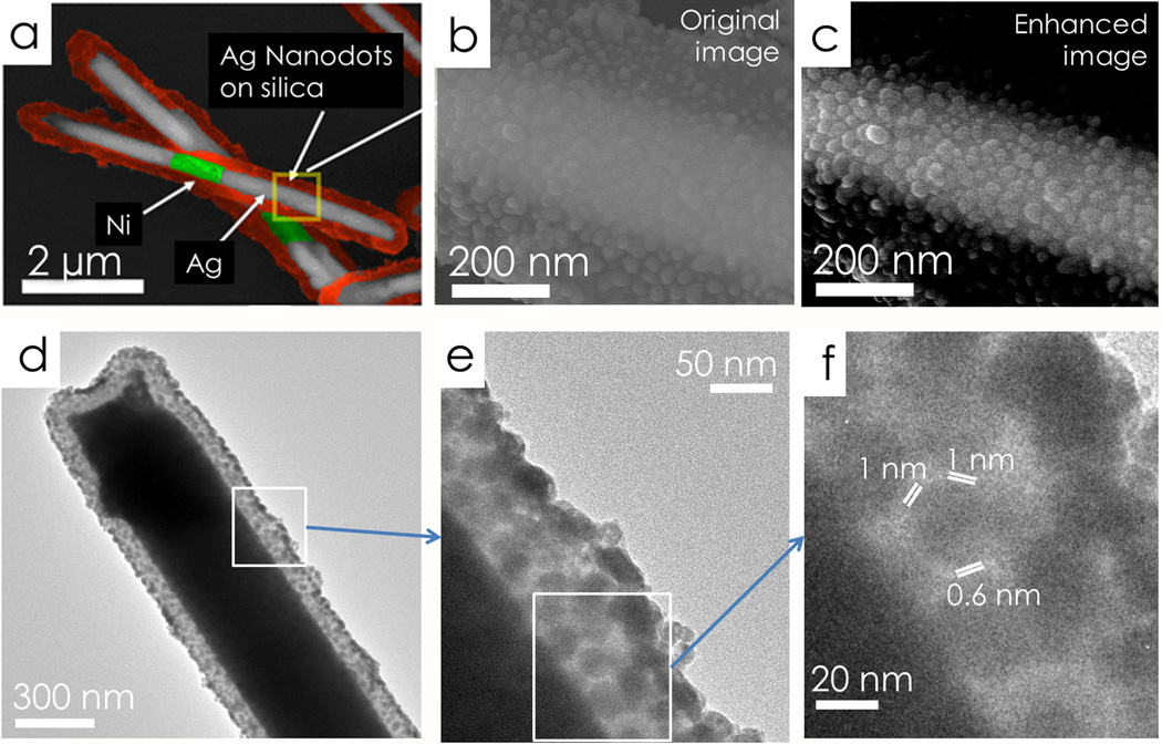
Next, the Ag/Ni/Ag nanorods were coated with 150 nm amorphous silica via hydrolysis of tetraethyl orthosilicate.[17] Here, the silica layers served as supporting substrates for synthesis of Ag nanodot arrays. Freshly prepared silver nitrate (AgNO3, 0.06 M, 400 µl), ammonia (NH3•H2O, 0.12 M, 400 µl), and nanorods (5.7 × 10⁸/ml, 400 µl) were mixed and stirred for 1 hour to let the silica adsorb adequate Ag ions before polyvinylpyrrolidone (PVP) (in ethanol, 10 ml of 2.5×10⁻⁵ M) was added. The reactant mixture was incubated at 70 °C to allow PVP to reduce ionic Ag into metallic Ag NPs on silica. After the 7-hour reaction, arrays of Ag NPs were obtained on the surface of the nanorods as shown in Figs. 1(a) and 1(b). By varying the reaction conditions, the average particle size can be tuned from 8 nm to 25 nm (supporting information S1). The highest enhancement of SERS was obtained from nanocapsules fabricated according to the conditions described above with a particle size of 25±6 nm as shown in the enhanced SEM image[18] in Fig. 1(c). Such nanocapsules offer an estimated Ag NP density of 1600/µm2. The junction sizes between the close neighboring NPs were analyzed with methods given by the supporting materials S1. If we only consider junctions of less than 2 nm between closely neighboring Ag NPs as hotspots, where the E field is much stronger than that on the Ag NPs or in wider junctions, the hotspot density is estimated to be 1200/µm2. TEM images evidenced large arrays of narrow junctions (< 2 nm) in Fig.1 (d–f).
Figure 1.
Color enhanced SEM images of tri-layer nanocapsules at (a) low magnification and (b) high magnification. (c) The contrast enhanced image of (b). (d–e) TEM images of a typical nanocapsule show a fairly uniform distribution of Ag NPs. (f) Arrays of junctions of the Ag NPs <2 nm.
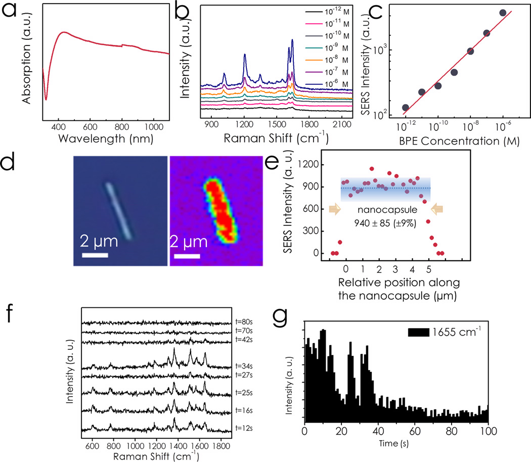
Before characterizing the SERS sensitivity of the nanocapsules, we studied the optical absorption of the nanocapsules to determine the optimal condition for SERS sensing. Here the Ag/Ni/Ag metal-cores were removed with the understanding that most excitation light was absorbed by the outermost Ag nanodot layers while little energy actually goes to the metal cores. The nanocapsules exhibited an absorption peak at 450 nm due to the collective plasmonic resonance of assembled Ag NPs [Fig. 2(a)].[19] Since the absorption was very sensitive to both the size and geometry of nanoparticles, it showed a broad background due to the size and shape distribution of the Ag NPs. With available lasers from 532–633 nm, a 532 nm laser (random polarized) was chosen as the excitation source for Raman scattering measurement because the wavelength of 532 nm is closer to the absorption peak and laser energy can be more effectively absorbed by the nanocapsules, which results in high intensity E-field focused at the hot spots and thus high EF for SERS detection. Indeed, the nanocapsules detected Raman spectra of 1,2-bi-(4-pyridyl) ethylene (BPE) with a concentration as low as 10−12 M (1 pM) [Fig. 2(b)]. The intensity of the SERS at 1644 cm−1 logarithmically increased with the concentration of BPE from 1 pM to 1 µM as shown in Fig. 2(c). The experimental details can be found in supporting information S2).
Figure 2.
(a) Optical absorption of the tri-layer nanocapsules; (b) SERS characterization of BPE from 1 pM to 1 µM shows clear SERS spectra; (c) SERS intensity increases with BPE concentrations; (d) Raman mapping profile of 1 µM R6G dispersed on a tri-layer nanocapsule shows uniform SERS intensity on the entire surface of the nanocapsules. (1655 cm−1, scan step 250 nm, integration time 0.5s) (e) SERS intensity distribution along the nanocapsule. (f) Variation of SERS spectra of R6G molecules in a 100-sec time frame with 1-sec integration for each spectrum. (g) Intensity of SERS at 1655 cm−1 as a function of time.
We further evaluated the SERS EF of the nanocapsules. The EF of the nanocapsules was measured and estimated to be 1.1×10¹⁰ following a widely used method[14a, 15] as described in supporting information S3. According to the bi-analyte and temperature-dependent SERS vibrational pumping methods, an EF of the order of 107–108 is sufficient for detection of single molecules of various analytes.[20] A SERS substrate with EF of 5×10⁹ has detected a single BPE molecule.[21] Therefore, the high EF value found in the nanocapsules suggests their single-molecule sensitivity. Moreover, we observed both a strong intensity and frequency fluctuation of Raman spectra from extremely low-concentration R6G (1 pM), which are consistent with single-molecule behaviors attributed to molecular diffusion into and out of hotspots [Fig. 2(f–g) and supporting information S4], according to previous reports.[7, 22] As a result, the SERS characterizations have placed the sensitivity of the nanocapsules in the single molecule regime, even though they are not absolute proofs.[22a]
Raman mapping of R6G shows that SERS enhancement was fairly uniform on the nanocapsules. At a concentration of 1 µM, R6G forms a monolayer on the nanocapsules (Experimental details can be found in supporting information S2). Different colors in the Raman mapping represent different Raman intensities of R6G. The Raman intensity at 1655 cm−1 was essentially uniform along the axis of the nanocapsules and reduced to zero towards the edges of the nanocapsules due to the deflated laser on the edges [Fig. 2(d)]. Analysis along the nanocapsules shows that the variation of the Raman intensity (at 1655 cm−1) is within ±9% [Fig. 2(e)]. This low variation suggests that the nanocapsules can readily detect monolayer analyte with good repeatability and predictability over their entire surface. Note that the tolerance of detection is actually less than ±9% since the coverage of R6G on nanocapsules cannot be absolutely uniform. Two factors determine this uniformity: (1) the controlled sizes and spacing of the Ag NPs, which gives relatively low variation of EF among hotspots; (2) the large number of hotspots of around 240 in each detection area [1200/µm2 (hot spot density) × 0.2 µm (1/3 of nanocapsule diameter due to nanocapsule curvature)× 1 µm (laser spot size)]. As a result, the SERS effect is uniform along the nanocapsules because of the averaged EF from all the hotspots in each detection position. We further note that the uniform SERS detection demonstrated on our nanocapsules is for monolayer chemicals. With reduced concentration of the analyte (less than that of a monolayer), we should expect larger variation of SERS along the nanocapsules and the ultimate tolerance is determined by the difference of EF from individual hotspots on the entire nanocapsules.
Different from most previous reports of SERS sensing nanostructures, our Raman nanocapsule sensors are designed for facile assembly at designated locations. Previously, seek-and-find efforts are generally required for SERS sensing devices due to the randomness of hot-spots. The illogicality of these efforts has greatly hindered the development of SERS for realistic applications. It is highly desirable to assemble the hot-spots at designated locations for location-predictable biosensing. Previously, substantial efforts were carried out to tackle such a problem;[11–13] however, it remains a daunting task to obtain Raman sensors with reliable spatial accuracy. Here, we present how the strategical design of the nanocapsules facilitate the rational assembly of hot-spots for location-predictable Raman sensing by using electric tweezers, our recently invented and contactless nanomanipulation technique.
Electric tweezers is based on combined DC and AC electric fields for precision orientation and transport of metallic nanowires in aqueous suspension, the fundamentals of which have been reported elsewhere[16a, 16c–f, 23]. In brief, in a combined DC and AC electric (E) field, a longitudinal nanoparticle can be transported by the DC E field due to electrophoretic force and aligned by the AC E field due to dielectrophoretic force. The transport and alignment can be controlled completely independently by the DC and AC E fields, respectively. Applying the combined E fields in both X and Y directions with controlled duration, longitudinal nanoparticles such as nanowires can be readily transported along prescribed trajectories on a 2-D surface with a precision of at least 150 nm14a, 14d.
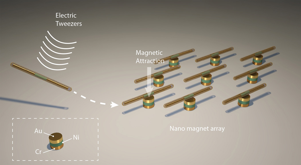
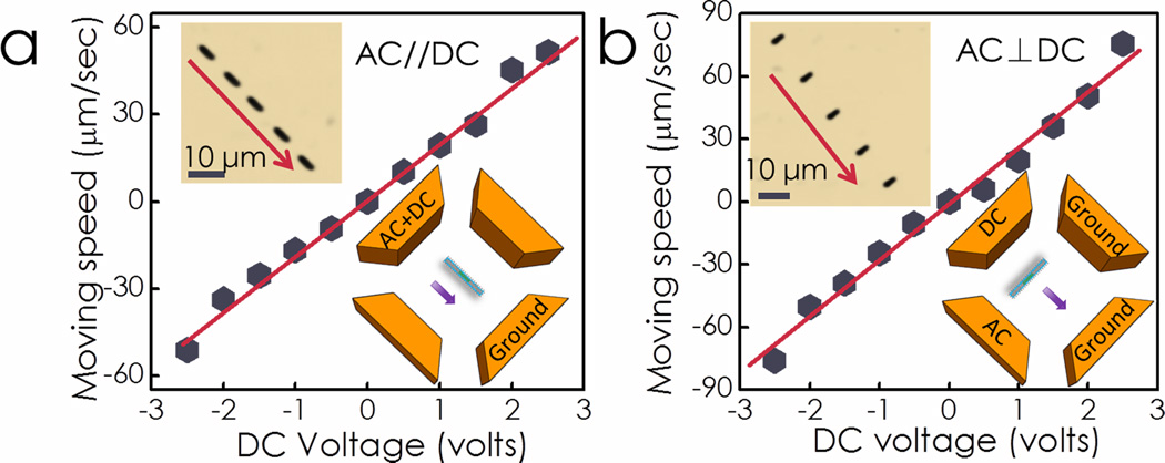
In this work, we leveraged the electric-tweezers manipulation technique and the unique magnetic Ni embedment in the Ag/Ni/Ag core of the nanocapsules to assemble an ordered plasmonic nanosensor array on prepatterned nanomagnets as shown in Scheme 3. Uniform AC and DC E fields were established in a quadruple microelectrode chip with two pairs of parallel-electrodes separated at a distance of 500 µm. At the center of the quadruple microelectrode, we fabricated a 3×3 nanomagnet array through standard e-beam lithography [Fig. 4(a)]. Each nanomagnet with diameter of 1 µm actually consists of a trilayer structure: 6 nm Cr adhesion layer on the substrate, 100 nm Ni layer providing magnetic fields, and 100 nm Au layer for tuning the magnetic interaction force. Nanocapsules suspended in D.I. water were dispersed at the center of the quadruple electrodes. The nanocapsules can be readily transported parallel [Fig. 3(a), AC//DC] or perpendicular to their orientations [Fig. 3(b), AC//DC], similar to earlier manipulation of Au nanowires[16a, 16d, 16e], by applying electric tweezers with a combined AC (15V, 20MHz) and DC voltages (−2.5V to +2.5V) on the quadruple electrodes,. The transporting speed linearly increased with the applied DC voltages for both orientations and reached approximately 80 µm/second at 2.5 V in vertical transport. We noticed that the Ag/Ni/Ag nanorod cores in the nanocapsules played a critical role in steering the transport orientations. After their metallic cores had been etched away,[24] the hollow nanotubes were transported by a DC E field; however, the orientations of the nanotubes were uncontrollable by AC E field due to the weak polarization and low alignment torques of insulating silica nanotubes in an AC E field (supplementary material S5). Therefore, it is essential to have the metallic Ag/Ni/Ag rod in the Raman nanosensors in order to facilitate steering of the orientation.
Scheme 3.
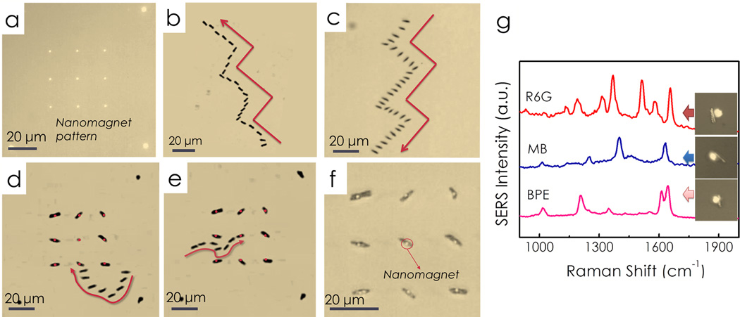
With the electric tweezers, nanocapsules can be transported and assembled onto a pre-patterned array of nanomagnets by utilizing the magnetic attraction force between the Ni segments in the nanocapsules and the magnetic layers inside the nanomagnets.
Figure 4.
Nanocapsules can be precisely transported and assembled on the nanomagnets with electric tweezers. (a) A 3×3 array of nanomagnets fabricated using E-beam lithography. With combined AC and DC E fields applied in both X and Y directions, nanocapsules were transported along prescribed trajectories such as “stairs” with (b) parallel and (c) transverse orientations. (d, e) Overlapped snapshots show the assembling process of a nanocapsule, where the nanomagnets were highlighted in red. The nanocapsules can be maneuvered and positioned at designated positions, showing the high flexibility and precision of the assembling. (f) An assembled 3×3 nanocapsules array. The bright nanomagnets are in the center of the nanocapsules, indicating that the attachment is due to the magnetic attraction between the Ni segments in the center of the nanocapsules and the magnetic layers in the patterned magnets. All the images were taken by reflective optical imaging. (g) From assembled nanocapsules, we have detected various chemicals including R6G, methylene blue, and BPE.
Figure 3.
AC and DC configurations on quadruple electrodes for the manipulation of nanocapsules. The nanocapsules are aligned in the direction of AC E field and transported in the direction of the DC E field. Nanocapsules were transported with controlled speed and orientation using "electric tweezers", (a) parallel (AC//DC) and (b) perpendicular (AC⊥DC) to their own alignment directions as shown in the overlapped optical images. Transporting speed is linearly proportional to the applied DC voltage.
After the nanocapsules were successfully transported in the microelectrodes, the next task was to assemble them on arrays of nanomagnets for location predictable SERS sensing. By programming the AC and DC E fields in both X and Y direction, we have compelled the nanocapsules to move along a prescribed trajectory, such as “steps”, with orientations either parallel [Fig. 4(b)] or perpendicular [Fig. 4(c)] to their transport directions. When nanocapsules were maneuvered into the vicinity of nanomagnets by the electric tweezers, the magnetic attraction force securely anchored the nanocapsules on the top of the nanomagnets. The magnetic force was between the nickel segments in the core of the nanocapsules and the Ni layer in the patterned nanomagnets on the chip. The manipulation of the nanocapsules was so versatile and precise that we easily maneuvered a nanocapsule to pass by a few neighboring nanomagnets and anchored it on a nanomagnet at the center of the array and other locations [Figs. 4(d) and 4(e)]. In this manner, we have assembled an array of nanocapsules on top of nanomagnets as shown in Fig. 4(f), where the bright circles indicate nanomagnets. A representative video clip of the assembling process is provided in the supporting information. Finally, from the assembled nanocapsule arrays, we successfully detected SERS of various chemicals including R6G, methyl blue and BPE and realized location predictable biochemical sensing by design as shown in Fig. 4(g). Note that the probability of single-molecule detection increases with the number of hot-spots on the nanocapsules excited by the laser. This can be readily achieved by increasing the size of the laser spot, having prescribed scanning along the nanocapsules, and even by trapping multiple nanocapsules on a single nanomagnet.
In summary, we rationally designed and fabricated a new type of nanocapsule SERS sensor to tackle the two great obstacles in the development of SERS technology: (1) the lack of a large quantity of hotspots with controlled gaps; (2) the difficulty of assembling SERS probes at designated locations. Our nanocapsule sensors consist of three functional layers. The outer sensing layers, made of large numbers of plasmonic NPs with controlled size and gaps, offer ultrasensitive SERS detection on the entire surface of the nanocapsules. The central silica coating layer provides support for the outer sensing layers and eliminates the plasmonic quenching effect. The inner metallic Ag/Ni/Ag core is the key component for steering the orientation of nanocapsules during manipulation by the electric tweezers. With electric tweezers, we have transported and anchored nanocapsules on patterned nanomagnet arrays due to the magnetic attraction between the Ni segment within nanocapsules and the patterned nanomagnets. As a result, an ordered array of Raman nanosensors has been rationally designed and fabricated for application in ultrasensitive and position-predictable SERS detections. Our design and fabrication of nanocapsules can provide valuable inspiration for investigating new types of Raman nanosensors to realize the full potential of SERS effect.
Supplementary Material
Acknowledgements
We are thankful for the facility support from Prof. Rodney S. Ruoff (Mechanical Engineering, University of Texas at Austin, TX, USA). We are grateful for the support of Welch Foundation (Grant No. F-1734) and National Institute of Health (NIH) under the Small Business Technology Transfer Research (STTR) program (Grant No. 1R41EB012885-01). We also thank Ms. Esther Huang and Anna Huang for proof reading the manuscript. ((Supporting Information is available online from Wiley InterScience or from the author)).
References
- 1.a) Bailo E, Deckert V. Chem. Soc. Rev. 2008;37:921. doi: 10.1039/b705967c. [DOI] [PubMed] [Google Scholar]; b) McMahon JM, Henry AI, Wustholz KL, Natan MJ, Freeman RG, Van Duyne RP, Schatz GC. Anal Bioanal Chem. 2009;394:1819. doi: 10.1007/s00216-009-2738-4. [DOI] [PubMed] [Google Scholar]; c) Camden JP, Dieringer JA, Wang Y, Masiello DJ, Marks LD, Schatz GC, Van Duyne RP. J. Am. Chem. Soc. 2008;130:12616. doi: 10.1021/ja8051427. [DOI] [PubMed] [Google Scholar]; d) Qin L, Zou S, Xue C, Atkinson A, Schatz GC, Mirkin CA. Proc. Nat. Acad. Sci. USA. 2006;103:13300. doi: 10.1073/pnas.0605889103. [DOI] [PMC free article] [PubMed] [Google Scholar]
- 2.Campion A, Kambhampati P. Chem. Soc. Rev. 1998;27:241. [Google Scholar]
- 3.a) Kneipp J, Kneipp H, McLaughlin M, Brown D, Kneipp K. Nano Lett. 2006;6:2225. doi: 10.1021/nl061517x. [DOI] [PubMed] [Google Scholar]; b) Kang T, Yoo SM, Yoon I, Lee SY, Kim B. Nano Lett. 2010;10:1189. doi: 10.1021/nl1000086. [DOI] [PubMed] [Google Scholar]
- 4.a) Kleinman SL, Ringe E, Valley N, Wustholz KL, Phillips E, Scheidt KA, Schatz GC, Van Duyne RP. J. Am. Chem. Soc. 2011;133:4115. doi: 10.1021/ja110964d. [DOI] [PubMed] [Google Scholar]; b) Xu HX. Appl. Phys. Lett. 2004;85:5980. [Google Scholar]
- 5.a) Qian XM, Nie SM. Chem. Soc. Rev. 2008;37:912. doi: 10.1039/b708839f. [DOI] [PubMed] [Google Scholar]; b) Nie S, Emory SR. Science. 1997;275:1102. doi: 10.1126/science.275.5303.1102. [DOI] [PubMed] [Google Scholar]
- 6.Moskovits M. Nature. 2011;469:307. doi: 10.1038/469307a. [DOI] [PubMed] [Google Scholar]
- 7.Michaels AM, Jiang J, Brus L. J. Phys. Chem. B. 2000;104:11965. [Google Scholar]
- 8.a) Liusman C, Li SZ, Chen XD, Wei W, Zhang H, Schatz GC, Boey F, Mirkin CA. Acs Nano. 2010;4:7676. doi: 10.1021/nn102495f. [DOI] [PubMed] [Google Scholar]; b) Jones MR, Osberg KD, Macfarlane RJ, Langille MR, Mirkin CA. Chem Rev. 2011;111:3736. doi: 10.1021/cr1004452. [DOI] [PubMed] [Google Scholar]; c) Banholzer MJ, Qin LD, Millstone JE, Osberg KD, Mirkin CA. Nature Protocols. 2009;4:838. doi: 10.1038/nprot.2009.52. [DOI] [PMC free article] [PubMed] [Google Scholar]; d) Qin LD, Park S, Huang L, Mirkin CA. Science. 2005;309:113. doi: 10.1126/science.1112666. [DOI] [PubMed] [Google Scholar]; e) Zheng GF, Chen XD, Mirkin CA. Small. 2009;5:2537. doi: 10.1002/smll.200901000. [DOI] [PMC free article] [PubMed] [Google Scholar]
- 9.Qin L, Banholzer MJ, Millstone JE, Mirkin CA. Nano Lett. 2007;7:3849. doi: 10.1021/nl072606s. [DOI] [PMC free article] [PubMed] [Google Scholar]
- 10.Banholzer MJ, Osberg KD, Li S, Mangelson BF, Schatz GC, Mirkin CA. ACS Nano. 2010;4:5446. doi: 10.1021/nn101231u. [DOI] [PubMed] [Google Scholar]
- 11.Huebner U, Schneidewind H, Cialla D, Weber K, Zeisberger M, Mattheis R, Moeller R, Popp J. Biophotonics: Photonic Solutions for Better Health Care Ii. 2010:7715. [Google Scholar]
- 12.Haynes CL, Van Duyne RP. J. Phys. Chem. B. 2001;105:5599. [Google Scholar]
- 13.Lee SJ, Morrill AR, Moskovits M. J. Am. Chem. Soc. 2006;128:2200. doi: 10.1021/ja0578350. [DOI] [PubMed] [Google Scholar]
- 14.a) Hu M, Ou FS, Wu W, Naumov I, Li X, Bratkovsky AM, Williams RS, Li Z. J. Am. Chem. Soc. 2010;132:12820. doi: 10.1021/ja105248h. [DOI] [PubMed] [Google Scholar]; b) Ou FS, Hu M, Naumov I, Kim A, Wu W, Bratkovsky AM, Li X, Williams RS, Li Z. Nano Lett. 2011;11:2538. doi: 10.1021/nl201212n. [DOI] [PubMed] [Google Scholar]
- 15.Schmidt MS, Hübner J, Boisen A. Adv. Mater. 2012;24:OP11. doi: 10.1002/adma.201103496. [DOI] [PubMed] [Google Scholar]
- 16.a) Fan DL, Cammarata RC, Chien CL. Appl. Phys. Lett. 2008;92:093115. [Google Scholar]; b) Fan DL, Zhu FQ, Cammarata RC, Chien CL. Appl. Phys. Lett. 2004;85:4175. [Google Scholar]; c) Fan DL, Zhu FQ, Cammarata RC, Chien CL. Appl. Phys. Lett. 2006;89:223115. [Google Scholar]; d) Fan DL, Zhu FQ, Cammarata RC, Chien CL. Nano Today. 2011;6:339. doi: 10.1016/j.nantod.2011.05.003. [DOI] [PMC free article] [PubMed] [Google Scholar]; e) Fan D, Yin Z, Cheong R, Zhu FQ, Cammarata RC, Chien CL, Levchenko A. Nature Nanotech. 2010;5:545. doi: 10.1038/nnano.2010.104. [DOI] [PMC free article] [PubMed] [Google Scholar]; f) Fan D, Zhu F, Cammarata R, Chien C. Phys. Rev. Lett. 2005;94 [Google Scholar]
- 17.a) Inaba S, Fujino S, Sakai K. Phys. Chem. Glass.-Euro. J. Glass. Sci. Tech. Part B. 2010;51:304. [Google Scholar]; b) Yi DK, Selvan ST, Lee SS, Papaefthymiou GC, Kundaliya D, Ying JY. J. Am. Chem. Soc. 2005;127:4990. doi: 10.1021/ja0428863. [DOI] [PubMed] [Google Scholar]; c) Graf C, Vossen DLJ, Imhof A, van Blaaderen A. Langmuir. 2003;19:6693. [Google Scholar]; d) Zhu YF, Shi JL, Shen WH, Dong XP, Feng JW, Ruan ML, Li YS. Angew. Chem. Int. Edit. 2005;44:5083. doi: 10.1002/anie.200501500. [DOI] [PubMed] [Google Scholar]
- 18.Processed by Image J. http://rsbweb.nih.gov/ij/index.html.
- 19.a) Amendola V, Bakr OM, Stellacci F. Plasmonics. 2010;5:85. [Google Scholar]; b) Liu ZX, Wang HH, Li H, Wang XM. Appl. Phys. Lett. 1998;72:1823. [Google Scholar]
- 20.Le Ru EC, Blackie E, Meyer M, Etchegoin PG. J. Phys. Chem. C. 2007;111:13794. [Google Scholar]
- 21.Blackie EJ, Ru ECL, Etchegoin PG. J. Am. Chem. Soc. 2009;131:14466. doi: 10.1021/ja905319w. [DOI] [PubMed] [Google Scholar]
- 22.a) Stranahan SM, Willets KA. Nano Lett. 2010;10:3777. doi: 10.1021/nl102559d. [DOI] [PubMed] [Google Scholar]; b) Weber ML, Litz JP, Masiello DJ, Willets KA. ACS Nano. 2012;6:1839. doi: 10.1021/nn205080q. [DOI] [PubMed] [Google Scholar]; c) Nie SM, Emery SR. Science. 1997;275:1102. doi: 10.1126/science.275.5303.1102. [DOI] [PubMed] [Google Scholar]; d) Lim D-K, Jeon K-S, Kim HM, Nam J-M, Suh YD. Nature Mater. 2009;9:60. doi: 10.1038/nmat2596. [DOI] [PubMed] [Google Scholar]; e) Dieringer JA, Lettan RB, 2nd, Scheidt KA, Van Duyne RP. J. Am. Chem. Soc. 2007;129:16249. doi: 10.1021/ja077243c. [DOI] [PubMed] [Google Scholar]; f) Michaels AM, Nirmal M, Brus LE. J. Am. Chem. Soc. 1999;121:9932. [Google Scholar]; g) Blackie EJ, Le Ru EC, Etchegoin PG. J. Am. Chem. Soc. 2009;131:14466. doi: 10.1021/ja905319w. [DOI] [PubMed] [Google Scholar]
- 23.Gao JH, Liang GL, Cheung JS, Pan Y, Kuang Y, Zhao F, Zhang B, Zhang XX, Wu EX, Xu B. J. Am. Chem. Soc. 2008;130:11828. doi: 10.1021/ja803920b. [DOI] [PubMed] [Google Scholar]
- 24.Xu X, Hasan D, Wang L, Chakravarty S, Chen RT, Fan DL, Wang AX. Appl. Phys. Lett. 2012;100:191114. doi: 10.1063/1.4714710. [DOI] [PMC free article] [PubMed] [Google Scholar]
Associated Data
This section collects any data citations, data availability statements, or supplementary materials included in this article.


