

Abstract
We report the implementation of an on-chip microscope system, termed fluorescence optofluidic microscope (FOFM), which is capable of fluorescence microscopy imaging of samples in fluid media. The FOFM employs an array of Fresnel zone plates (FZP) to generate an array of focused light spots within a microfluidic channel. As a sample flows through the channel and across the array of focused light spots, the fluorescence emissions are collected by a filter-coated CMOS sensor, which serves as the channel's floor. The collected data can then be processed to render fluorescence microscopy images at a resolution determined by the focused light spot size (experimentally measured as 0.65 μm FWHM). In our experiments, our established resolution was 1.0 μm due to Nyquist criterion consideration. As a demonstration, we show that such a system can be used to image the cell nuclei stained by Acridine Orange and cytoplasm labeled by Qtracker®.
In the past few years, there has been significant research and development in the area of chip-scale microscopy.1,2 An inexpensive, highly compact and easy-to-use chip-scale microscope can be an important lab-on-a-chip component for point-of-care medical systems, low-cost diagnostic tools for developing country applications, and high-throughput automated bioscience analysis systems. Furthermore, a high-resolution and generally usable fluorescence on-chip microscopy technique can significantly expand the utility range of such chip-scale microscopes, as the high sensitivity of the fluorescence signal detection and the broad array of fluorophore species and expression techniques available make fluorescence one of the most important read-out modes for microscopy.3
This recognition has driven a number of research efforts in developing a useful fluorescence on-chip microscopy technique. However, the incoherent nature of fluorescence and the need for high quality optical filters are significant design obstacles. Coskun et al.show that it is possible to superpose an indication of the fluorophore concentration sites onto brightfield in-line holography derived images of samples as long as the fluorophores are clustered and the clusters are well separated (by ~10 μm).4 A progression of that effort5 uses bundled fibers to collect and channel fluorescence to a sensor and was able to generate fluorescence images that have a claimed resolution of ~4 μm. Improving the technique's resolution to the point where sub-cellular fluorescence features are resolvable may prove challenging as finer fiber tips will further diminish the effective fluorescence collection angle and the light channeling efficiency.
In this paper, we report a chip-scale imaging method, termed fluorescence optofluidic microsope (FOFM), which adapts the scan-based imaging strategy of the optofluidic microscopy method to accomplish high-resolution fluorescence microscopy imaging. Compared with aperture based on-chip imaging platform developed in our group,6 this approach is highly efficient at fluorescence light collection. It is also capable of placing the plane of highest acuity at any desired height within the sample and its resolution can be adjusted by a straightforward alteration of its design's parameters. Our FOFM prototypes were able to achieve 0.60 μm full width at half maximum (FWHM) in the focused spot size for excitation wavelength of 405 nm and 0.65 μm for 488 nm excitation. The FOFM is particularly suitable for mass-manufacture in a semiconductor foundry, and therefore FOFM devices have the potential to be made very compactly and cost-effectively. In the next section, we will describe the FOFM's imaging principle. Then, we will describe the fabrication steps involved in our prototype construction. Next, we will discuss our characterization of the experimental results and report on our demonstration experiments that use our prototypes for fluorescence microscopy imaging of cells.
The FOFM basic design is centered around a microfluidic channel. An array of Fresnel zone plates (FZP)7 patterned on a metal layer forms the ceiling of the channel. Under uniform plane illumination with an appropriate excitation light source from the top, each FZP focuses light into a tight spot within the microfluidic channel. As a sample flows through the channel, this focused light spot will locally excite fluorophores within the sample. The fluorescence signal collection is accomplished by a low-cost CMOS sensor which is coated with a filter that effectively blocks the excitation light and that efficiently transmits fluorescence emissions well. The time varying fluorescence signal associated with each spot represents a single line scan across the sample. The FZP array spans the channel diagonally such that the distance between the adjacent scan lines is less than the FWHM of the point spread function of each focus. This assures that we can fully scan all parts of the sample and that by appropriately compositing all line scans, we can then generate a high-resolution fluorescence image of the sample at a resolution that is limited by the focused spot size.
We note that this OFM design uniquely enables fluorescence microscopy imaging, which is not achievable with earlier versions of OFM designs.1,6 For previous OFM designs, the effective plane of highest acuity is right above the sensor surface. The achievable image resolution degrades as a function of object-to-sensor separation.1 The placement of an optical filter layer on the sensor surface to accomplish fluorescence imaging would necessarily introduce an unacceptable separation and degrade the image resolution significantly. In this current FZP OFM design, the plane of highest acuity (where the light spots focus) can be set at arbitrary height within the microfluidic channel and, as such, can tolerate a significant object-to-sensor separation. This freedom allows us to place an appropriate optical filter on the sensor for fluorescence imaging purpose.
For each of our FOFM prototypes, we fabricated the FZP array on a 300 nm thick chrome layer that was plated on a quartz substrate. Each FZP is composed of a series of transparent and opaque concentric rings.7 To create the focus at a focal length f the zones should switch from opaque to transparent at radii
| (1) |
where k is an integer, λ is the wavelength of the light and n is the refractive index of the medium in which the focus is formed. The resolution, δ,7 of a focal spot of a zone plate depends on the smallest zone width
| (2) |
where ΔrK is the outer most zone width, which is determined by the fabrication limit. In our case, the FZP pattern was defined by electron beam lithography with a minimum achievable line width of 400 nm. The depth of the focus Δ,8 defined the half distance between two adjacent axial intensity minima of a FZP focus, can be calculated as
| (3) |
where N is the number of transparent zones, which is 5 in our design. Fig. 1(c) shows a scanning electron microscopy image of a single FZP in our prototypes. The distance between each FZP was 20.8 μm - this corresponds to the length of 4 sensor pixels on the CMOS sensor. The exact FZP ring parameters are governed by eqn (1) and they differ between the two groups of FOFM prototypes we implemented. The designed focal length was 13 μm and the diameter of each FZP was 15 μm. One group was designed to work at an excitation wavelength of 405 nm and the other at an excitation wavelength of 488 nm.
Fig. 1.

(a) Schematics of the Fresnel zone plate based Fluorescence Opto-fluidic Microscope (FOFM). A sample flows in the microfluidic channel on top of the filter coated image sensor. The Fresnel Zone Plate array creates an array of foci inside the channel. (b) Schematic of the device (top view). The Fresnel zone plates are defined on the top floor of the microfluidic channel and span across the whole microfluidic channel (blue lines). (c) SEM image of a Fresnel zone plate. (d) Photograph of our FOFM prototypes.
To verify the focus quality, we observed the focus formed by the FZP by a 40X, 0.85 N.A. water immersion microscope objective. Here we used the water immersion microscope objective to match the refractive index of the medium in the microfluidic channel. A piece of the top plate with FZP arrays was mounted on a vertical motorized stage. The stage moved with a step size of 0.5 μm, and a camera captured images of the focus at each step. Fig. 3 shows the experimental results. The FWHM of the focus was 0.60 μm for 405 nm excitation, and 0.65 μm for 488 nm excitation, which were slightly larger than the theoretical value of 0.5 μm. The focal depth for the 405 nm version was 4.0 μm, and the focal depth for the 488 nm version was 3.5 μm.
Fig. 3.
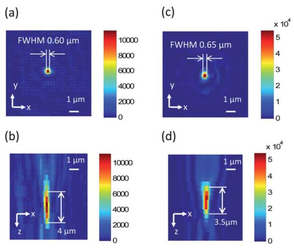
The intensity profile of the focus generated by Fresnel zone plate. (a) The intensity of the focus at the focal plane by 405 nm excitation. (b) The depth-wise cross-section of the intensity of the focus by 405 nm excitation. (c) The intensity of the focus at the focal plane by 488 nm excitation. (d) The depth-wise cross-section of the intensity of the focus by 488 nm excitation.
The base of each of our FOFM prototypes was a monochromatic CMOS sensor. The sensor (Aptina, MT9M001) consists of 1280 × 1024 pixels of size 5.2 μm. Prior to usage, we removed the glass cover to allow direct sensor surface access. We then planarized the sensor surface with a layer of Poly(methyl methacrylate) (PMMA).
Next we coated the sensor with an appropriate filter layer. The FOFM filter layers consisted of an appropriate filter pigment dissolved in a photo-resist based material and patterned and cured directly onto the sensor. Two different filter pigments, Aptina green1 and Aptina red1 (provided by Aptina Imaging), were used. The transmission spectra of the filter materials are shown in Fig. 2. The green filter is a band pass filter that provides an optical density (OD) difference of about 6 between 488 nm excitation and 520 nm emission at a filter thickness of 8 μm. The red filter, which transmits the wavelength above 560 nm, provides an OD difference of 9 between 405 nm excitation and 625 nm emission for a filter thickness of 6 μm.
Fig. 2.

The transmission spectrum of 6 μm thick red filter layer and 8 μm thick green filter layer. The arrows indicate the emission peaks of Acridine Orange and Qdot 625. The 405 nm and 488 nm excitation lines are also marked for reference.
The microfluidic channel was fabricated using polydimethylsiloxane (PDMS).9 A stamp with positive channel pattern was defined by the photo-resist SU-8 (2015, Microchem Inc.) on a glass substrate. A spin coater coated a 20 μm thick SU-8 layer at a spin speed of 1700 rpm. An uncured PDMS droplet was placed on the sensor. The channel on the stamp was set at an angle of 0.03 radian to the direction of a row of the pixels. This ensured that adjacent FZPs overlapped each other by 0.5 μm across the width of the channel (see Fig. 1(b)). The stamp was then pressed onto the sensor while applying the heat. The PDMS was cured at 85 °C with 15 min bake time. After the removal of the stamp, a profiliometer measured the depth of the channel. This process introduced an extra layer of PDMS underneath the channel.10 The thickness of the layer was measured to be 2–3 μm. Finally a mask aligner (MJB3, Karl Suss) aligned an FZP array to the fabricated sensor chip with the microfluidic channel and filter layer.
In our demonstration a 488 nm laser (Cyan OEM488 nm, Spectra-Physics) and a 405 nm laser (OEM Laser System Inc.) were used as the excitation sources for the FOFM. The power at each FZP generated focal spot was about 10 μW. During operation, the imaging frame rate was 1 kHz.
Finally, in all of our FOFM prototypes, we opened a window in the chrome layer of the channel ceiling. Under illumination with a white LED (MCWHL2, Thorlabs Inc.), we were able to capture 200 frames of low-resolution brightfield images of sample flowing through that segment of the microfluidic channel. These images can then be processed to form a higher-resolution image by using the sub-pixel resolving OFM (SROFM) method described in ref. 11 The SROFM method's resolving ability degrades as a function of sample-to-sensor separation. Since the FOFM sensor chips were coated with a ~13 μm thick layer of filter material and PDMS material, the acquired SROFM images are relatively low in resolution. Nevertheless, they could be used to provide outlines of the samples imaged. In applications where high-resolution brightfield microscopy images are required, the on-chip microscope can be designed to exclude the filter material from the SROFM portions of the sensor chip.
To verify the proper operation of our FOFM prototypes, we first conducted a verification experiment by employing an FOFM device to image a control which consisted of a fluorescence microsphere of diameter 8 μm (DG06M, Bangs Laboratories Inc.). The fluorophores were evenly distributed within the sphere. The excitation wavelength used was 488 nm and the center emission fluorescence wavelength was 520 nm. Since we know the power distribution associated with each focused light spot from the data presented in Fig. 3, we can calculate the expected fluorescence emission measured by the sensor pixels as the microsphere traverses a single focused light spot. We compared the result derived from a calculation to our experimental results as shown in Fig. 4. The good agreement verified the proper operation of our FOFM prototypes.
Fig. 4.
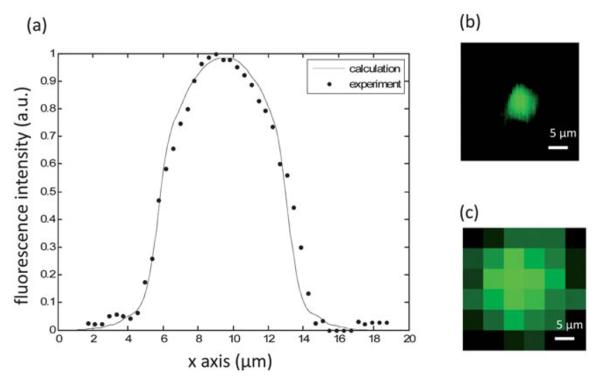
(a) A line trace of a fluorescence microspheres by a single FZP, comparing to the calculation result. (b) The fluorescence image of a fluorescence microsphere collected by FOFM. (c) The fluorescence image of a fluorescence microsphere by direct readout from the sensor with uniform illumination.
We next employed our FOFM prototypes to image fluorescence stained cells. The cell samples used in the experiments were suspended HeLa cells (CCL-2, ATCC). We prepared two types of stained cells. In one preparation, we loaded quantum dots (QDs) in the cytoplasm with Qtracker® 625 Cell Labeling Kit (A10198, Invitrogen). The kit uses a custom targeting peptide to deliver Qdot 625 into the cytoplasm of live cells.12 Qdot 625 can be excited at 405 nm and has an emission peak wavelength of 625 nm. In a second preparation, we stained the nuclear content of the cells with Acridine Orange (A1301, Invitrogen). For this, we incubated live cells with 20 μg ml−1 Acridine Orange solution (PBS buffered) for 5 min and triple rinsed with PBS before imaging. Acridine Orange can be excited at 488 nm and has an emission peak at 525 nm. We flowed the stained cells in our FOFM prototypes to acquire fluorescence images.
The flow speed was approximately 500 μm s−1, and the frame period was 1 ms, corresponding to the displacement of 0.5 μm per frame. Each sample's flow speed uniformity was monitored by the SROFM segments of the prototypes, and the yield rate was comparable to those of earlier OFM systems.1 The green filter coated FOFM captured images of the Acridine Orange stained cells, and the red filter coated FOFM captured images of the Qtracker® stained cells. The fluorescence images captured by FOFM prototypes were superimposed with the super-resolution bright field images. Fig. 5 shows images of the HeLa cell nuclei stained by Acridine Orange. The fluorescence signal is concentrated within the center of a cell. Fig. 5 also shows the images of the HeLa cytoplasm labeled by Qtracker®. The Qtracker contrast agents are non-specific-binding quantum dots. The Qtracker stain pattern is expected to vary from cell to cell. We also acquired images with a conventional microscope operating with a 20× 0.4 N.A. objective for comparison (Fig. 5d, h). We can see that the fluorescence images acquired with the FOFM prototypes agree with those acquired with a conventional fluorescence microscope.
Fig. 5.

Fluorescence images of stained HeLa cells collected by FOFM. (a–c) The fluorescence images of Acridine Orange stained HeLa cells acquired by FZP FOFM superimposed on defocused bright field SROFM images to provide the outline. (e–g) The fluorescence images of Qtracker labled HeLa cells acquired by FZP FOFM superimposed on defocused bright field SROFM images. (d,h) The fluorescence image superimposed on a bright field image acquired by a conventional 20X 0.4 N.A. microscope.
We note that the FOFM's resolution is fundamentally set by the FZP's focused spot size. However, in our prototypes, our sampling step-sizes in both x- and y-axis impose a resolution limit of 1 micron to our fluorescence images due to Nyquist sampling criterion considerations.13 To achieve the resolution set by the FZP's focused spot size, we would need to increase the sampling frame rate and increase the line scan overlap by approximately a factor of 2 each. There is no technological limitation that prevents these improvements. We simply designed our FOFM prototypes conservatively in our experiments.
At this point, we would like to point out several features of our FOFM design that are worth noting.
First, the choice of using a filter coated CMOS sensor to serve as the device's floor carries two advantages. Specifically, we can optimally collect fluorescence from the sample without requiring the use of a more elaborate collection optics scheme. The FOFM design can collect almost all fluorescence from the bottom semi-sphere of an isotropic fluorescence source, which is close to 50% of the total emission. In contrast, a 0.65 N.A., 40× microscope objective is only able to collect ~12% of the total emission. In addition, this simple planar and monolithic collection design is very compatible with semiconductor mass-manufacture.
Another noteworthy point of this FOFM design is that, by spacing the FZP apart from each other at an adequate distance, it is possible to separate the detected fluorescence associated with each focused spot by the CMOS sensor without ambiguity. More interestingly, if the approximate size of the sample is known, we need only space the FZP at a distance larger than the sample size to guarantee that cross-talk is absent - in this case, only one focused spot can interrogate the sample at any given time and any signal we see on the sensor can be automatically attributed to that focused spot. In fact, our FOFM prototypes made good use of this design point. A thick layer of filter material and PDMS separates the sensor pixels from the channel: the overall thickness was about 13 microns. The fluorescence from a fluorophore in the center of one of the focused light spot would spread over an area of diameter at least 30 μm (or 6–7 sensor pixel lengths) on the sensor. This implies that at our FZP-to-FZP distance of 20.8 μm, fluorescence signal associated with adjacent focused light spots could overlap and contribute cross-talk to each other. The cells used in our experiments are less than 20 μm in diameter and, as such, only one focused light spot can excite a given cell at anytime and we were able to avert cross-talk problems. To work with large cells or samples, we simply would need to increase the FZP-to-FZP distance.
On a different note, it is worth contrasting the use of an FZP array with the use of a conventional lenslet array in the FOFM design. The FZP fabrication process is compatible with semiconductor mass-manufacture. This is a relevant consideration as we envision the mass-manufacture of OFM to occur in semiconductor foundries. Further more, the FZP approach allows for the generation of tight focus spot with short focal length that would be very difficult to accomplish with a refractive optical element. As a case in point, if we are to replace one of the FZP elements in our prototype with a ball lens of the same diameter, the ball lens would have to possess a refractive index of at least 2.7 (in comparison to quartz glass, which has a refractive index only 1.45 in the optical band) to achieve the same focal length. The FZP approach does come at a flexibility price, since the focal length of the FZP depends strongly on the optical wavelength. As such, each FOFM needs to be designed with a specific excitation wavelength in mind. Finally, our current FZP is able to direct ~10% of the incident light into the focused spot. If application requirements demand higher efficiency, the current binary FZP can be switched to a binary phase FZP, which has 40.4% (4/π2) efficiency, or a Fresnel lens, which in principle can reach 100% efficiency.
In summary, we described the imaging principle and fabrication methods of the FOFM system based on an FZP arrays. We demonstrated the imaging ability of our FOFM prototypes by imaging HeLa cell nuclei stained by Acredine Orange and HeLa cytoplasm labeled by Qtracker® 625. The resolution of such systems is limited by the focused spot size of the FZP. For our prototype, these are 0.60 μm for 405 nm, and 0.65 μm for 488 nm excitation. This FOFM design intrinsically achieves high fluorescence collection efficiency and its planar and monolithic design should allow straightforward semiconductor foundry-based mass manufacture.
Acknowledgements
We would like to express our thanks to Guoan Zheng, Seung Ah Lee, Dr Jigang Wu, Dr Benjamin Judkewitz, Rick Lake, Dr Marc Sulfridge, and Dr Swarnal Borthakur for the discussions and their generous help. We acknowledge support from the Gates Foundation and a generous gift from Aptina Imaging.
References
- 1.Cui X, Lee LM, Heng X, Zhong W, Sternberg PW, Psaltis D, Yang C. Proc. Natl. Acad. Sci. U. S. A. 2008;105:10670. doi: 10.1073/pnas.0804612105. [DOI] [PMC free article] [PubMed] [Google Scholar]
- 2.Heng X, Erickson D, Baugh LR, Yaqoob Z, Sternberg PW, Psaltis D, Yang C. Lab Chip. 2006;6:1274–1276. doi: 10.1039/b604676b. [DOI] [PubMed] [Google Scholar]
- 3.Tsien RY, Ernst L, Waggoner A. Handbook of biological confocal microscopy. 2006. pp. 338–352. [Google Scholar]
- 4.Coskun AF, Sencan I, Su TW, Ozcan A, Mylonakis E. PLoS One. 2011;6:896–903. doi: 10.1371/journal.pone.0015955. [DOI] [PMC free article] [PubMed] [Google Scholar]
- 5.Coskun AF, Sencan I, Su TW, Ozcan A. Analyst. 2011;136:3512–3518. doi: 10.1039/c0an00926a. [DOI] [PMC free article] [PubMed] [Google Scholar]
- 6.Pang S, Cui X, DeModena J, Wang YM, Sternberg P, Yangab C. Lab Chip. 2010;10:411–414. doi: 10.1039/b919004j. [DOI] [PMC free article] [PubMed] [Google Scholar]
- 7.Young M. J. Opt. Soc. Am. 1972;62:972–976. [Google Scholar]
- 8.Sussman M. Am. J. Phys. 1960;28:394–398. [Google Scholar]
- 9.Xia YN, Whitesides GM. Annu. Rev. Mater. Sci. 1998;28:153–184. [Google Scholar]
- 10.Heckele M, Schomburg WK. J. Micromech. Microeng. 2004;14:R1. [Google Scholar]
- 11.Zheng G, Lee SA, Yang S, Yang C. Lab Chip. 2010;10:3125–3129. doi: 10.1039/c0lc00213e. [DOI] [PubMed] [Google Scholar]
- 12.Umezawa N, Gelman MA, Haigis MC, Raines RT, Gellman SH. J. Am. Chem. Soc. 2002;124:368–369. doi: 10.1021/ja017283v. [DOI] [PubMed] [Google Scholar]
- 13.Oppenheim AV, Schafer RW. Discrete-Time Signal Processing. 2nd Edition Prentice Hall; 1998. p. 146. [Google Scholar]