Abstract
In pondering of new promising transparent conductors to replace the cost rising tin-doped indium oxide (ITO), metal nanowires have been widely concerned. Herein, we demonstrate an approach for successful synthesis of long and fine Cu nanowires (NWs) through a novel catalytic scheme involving nickel ions. Such Cu NWs in high aspect ratio (diameter of 16.2 ± 2 nm and length up to 40 μm) provide long distance for electron transport and, meanwhile, large space for light transmission. Transparent electrodes fabricated using the Cu NW ink achieve a low sheet resistance of 1.4 Ohm/sq at 14% transmittance and a high transparency of 93.1% at 51.5 Ohm/sq. The flexibility and stability were tested with 100-timebending by 180°and no resistance change occurred. Ohmic contact was achieved to the p- and n-GaN on blue light emitting diode chip and bright electroluminescence from the front face confirmed the excellent transparency.
Transparent electrodes (TEs) which conduct electrical current and allow light to pass through are widely used as the essential component in various optoelectronic devices such as light-emitting diode, photovoltaic cells, photodetectors, solar control windows and touch screens1,2,3,4. As the name implies, an excellent TE itself ought to possess high conductivity and high transparency. Meanwhile, from an application point of view, low resistance between TE and active electronic materials which are generally semiconductors, also plays a crucial role in achieving high-performance devices. Over the past few decades, promising TE materials that have come on stage include transparent conductive oxides, metal grids5, metal nanowire (NW) networks6 and graphene3. Tin-doped indium oxide (ITO) is the best transparent conductive oxide layer with the lowest resistivity on a commercial scale7, which has been the prevailing material in flat-panel displays. However, ITO is too expensive owing to the high cost of indium. In addition, ITO thin films are too brittle to be used in flexible devices8 and low optical transmittance in blue wavelength regions6. Nanoscale carbon-based materials9 such as graphene have recently come up with exceptionally high mobility and excellent transparency10,11. However, handicaps of large amount of grain boundaries and wrinkles formed during growth lead to the limitation of graphene sheet resistance (100–1000 Ohm/sq at 80–90% transmittance)12. Moreover, the substrate-based synthesis by chemical vapor deposition (CVD) has to face challenges in large-scale production at low cost. Another possibility is offered by metallic nanograting patterns prepared by roll-to-roll nanoimprint lithography13 or metal patterning method14. In respect to TEs composed of metallic nanostructures, interlaced metal NW networks seem to hold a greater promise, which have well met most of the TE requirements such as good performance, mass synthesis (through solution method) and low cost. Since the initial work reported by P. Peumans et al, wherein TEs with a performance exceeding that of conventional metal oxide were prepared using Ag NW mesh, interlaced metal NW networks have attracted increasing attentions15. For example, large area Ag NWs network with a sheet resistance of 50 Ohm/sq at 90% transmittance was achieved by Scardaci, V. et al.16, meanwhile more excellent performances of R = 34 ± 2 Ohm/sq at 98% transmittance and 8 ohms/sq and 80% diffusive transmittance in the visible spectral range for silver nanowires electrodes were reported by Leem, D.-S. et al17 and Y. Cui's group18, respectively. Wiley and co-workers have been focusing their attention in Cu nanowires TEs, who obtained a sheet resistance 61 Ohm/sq at 67% transmittance for Cu NWs TEs19 and then improved the optoelectronic performance to 60 Ohm/sq at 94.4%20. Furthermore, in order to optimize the oxidation-resistant ability of the Cu NWs TEs, they coated Cu NWs with Ni shell. A more effective solution was offered by coating layers of aluminum-doped zinc oxide onto the electrospun copper nanofibers21. More recently, based on electrospinning and metal deposition, transparent conductive electrode with remarkable optoelectronic performance (sheet resistance of about 2 Ohm/sq at 90% transmission) and mechanical flexibility was achieved in Y. Cui's group22. The obviously contradicting relationship between the high transmittance and low resistivity in metal NW networks strongly restricts its further improvement and wide applications, which has been a crucial problem to overcome. Where does this conflict stem from? It was observed that the thicker the NW layer is, the higher the conductivity of TE could be but the worse the transmittance would become meanwhile23. This is because the light has been largely blocked by the thick media. Recently, metal nanowires include Ag NWs24, Cu NWs19,25 and Cu@Ni core-shell NWs26, have been synthesized through chemical solution route. These metal NWs in the form of inks were then imprinted onto substrates to form desired TEs. According to previous reports, the metal NWs generating in solution usually have large diameter, short length and a great number of nanoparticles attached27. For example, the Ag NWs synthesized by Lee et al. have a diameter between 100 ~ 150 nm24. The Cu NWs reported by Wiley et al. are in a diameter of 90 ± 10 nm and in a length of 10 ± 3 μm, meanwhile, spherical nanoparticles are absorbed at the end of the NWs19. As a result, the transparent conductor consisting of the as-synthesized Cu NWs has a sheet resistance of 61 Ohm sq−1 at a transmittance of just 67%. On this issue, Hu and his coworkers proposed the percolation theory to predict the threshold areal NW density of Nth = (4.236/L)2/π (L being the wire length) for achieving the onset of TE conductivity23. From this relation, we can know that a longer wire length could provide a higher conductivity with less NWs. Furthermore, a network with thinner NWs is also beneficial to give wider spacing as the light's pathway. Thus, an important solution to the conflict and the crucial challenge lies in producing perfectly ultra-long and thin metal NWs with smooth surfaces27.
Catalytic effect has been widely used by chemists to synthesize a variety of chemical compounds since this concept was recommended to chemical science by Berzelius in the 18th century. Based on this concept, here we demonstrate a novel method with nickel ions to large-scale catalytic synthesis of ultra-long and fine Cu NWs in hydrophobic solution with excellent dispersibility and very high aspect ratio. The catalytic growth mechanism and network connection model were further elucidated, which could be extended to synthesis of other metallic NWs such as Ag and Au NWs. The imprinted TE with the as-prepared Cu NWs achieves a sheet resistance of 51 Ohm sq−1 at 93% transparency, which has been comparable to the commercial ITO thin film and exceeded some of the available metal-based TEs (see Supplementary Information, Fig. S1). Moreover, Ohmic contact to n- and p-type GaN conducting layers have been fabricated and succeeded in electroluminescence of GaN-based blue light emitting diodes (LEDs).
Results
Synthesis and characterization of Cu NWs
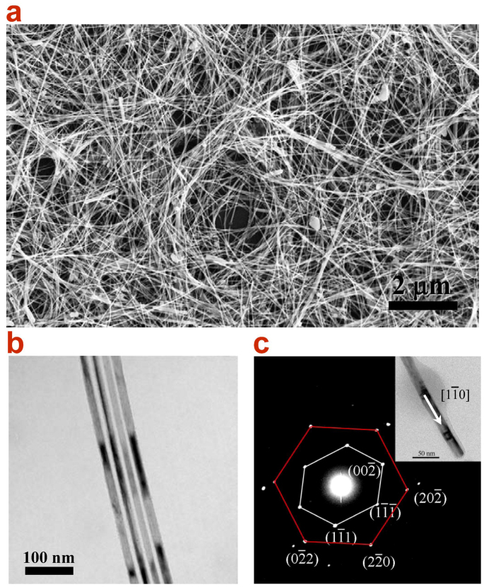
In a typical experimental procedure, Cu NWs with high aspect ratios were synthesized in Oleylamine solution through a Ni(acac)2 catalytic formation process. A representative SEM image of the as-grown Cu NWs is presented in Fig. 1a. It demonstrates that the Cu NWs have a uniform diameter and are well dispersed. No particle-like structure which will be less conductive or large-scaled bundles forming by the aggregation of Cu NWs is observed. From the SEM image in a vaster scale (see Supplementary Information, Fig. S2), it can be seen that these Cu NWs possess an entire length up to 40 μm. This is critical for improving the conductivity of a single Cu NWand reducing the overall resistivity of NW networks, which will be further discussed below. Figure 1b shows the TEM image of the Cu NWs, illustrating that there is a uniform diameter distribution throughout all NWs. The average diameter is only 16.2 ± 2 nm (averaged over 55 NWs randomly selected from TEM images, see Fig. S3a), which is quite fine compared to former reports, e.g. ~ 24 nm for Cu NWs synthesized by glucose reduction of CuCl2 in the presence of hexadecylamine25, ~ 50 nm for Cu NWs prepared in the organic phase through the controlled disproportionation of Cu(I)28 and ~ 79 nm for Cu NWs synthesized via a self-catalytic growth process within a liquid-crystalline medium of hexadecylamine and cetyltriamoninum bromide29. Although ultra-thin they are, these NWs show an excellent flexibility and some of them can endure a nearly 180° bending without being broken (Fig. S3b). This feature can contribute to a Cu NW electrode suitable for highly flexible film as flat-panel display. The selected area electron diffraction (SAED) pattern (Fig. 1c) obtained from an individual Cu NW shown in the inset shows two sets of separated diffraction patterns which can be assigned to the [110] and [111] zone axes of face-centered cubic (fcc) structure, respectively. The superposition of blended diffraction spots30 indicates a five-fold twinned pentagonal structure of the Cu NW that has a [1 0] growth direction. This twinned pentagonal structure is an important factor for the high mechanical strength and high electrical conductivity of the Cu NWs according to the viewpoint presented by Lu et al31.
Figure 1.
(a) SEM and (b) TEM images of Cu NWs synthesized by the Ni(acac)2 catalytic procedure. The ultra-long, super-fine and uniform NWs can be observed, which show an average diameter of 16.5 nm. (c) SAED pattern of an individual Cu NW (inset). Two sets of diffraction patterns show the five-fold twinned pentagonal structure of the Cu NW and indicate the growth along the [1–10] direction.
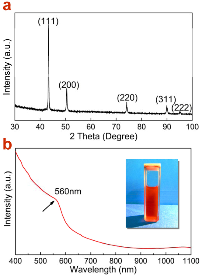
In order to characterize their stability, the as-synthesized Cu NWs had been exposed in air at room temperature for 100 days and the X-ray diffraction (XRD) pattern was then recorded (Fig. 2a). The peaks at 2θ = 43.3, 50.4, 74.2, 90.0 and 95.2° correspond to the diffractions from the {111}, {200}, {220}, {311} and {222} crystalline planes of fcc Cu (JCPDS #03-1018). No additional peaks relating with Ni, CuNi alloy or CuO were observed, indicating the high chemical purity and high stability of these NWs. The absence of Ni can be confirmed by the red color of the dispersing solution of Cu NWs (Fig. 2b inset)32 and energy dispersive X-ray spectroscopy (EDS) (see Supplementary Information, Fig. S4). Fig. 2b further shows the UV-Vis-NIR extinction spectra of the Cu NWs dispersed in hexane, from which an absorption peak locating at 560 nm is observed. The weak peak may result from the fact that the surface plasmon resonance band of the Cu NWs locating in the region of the interband transitions (below 590nm) because of the small diameter of Cu NW. It is meaningful for the high transmittance of the Cu NW networks33. Meanwhile, only the transverse SPR mode is observed in the extinction spectra because the peak from longitudinal plasmon resonance may red-shift to the far infrared band which is beyond the detection range of the UV-Vis-NIR spectrophotometer. This phenomenon also qualitatively reflects the representative properties of the large length-to-diameter ratio of the as-prepared Cu NWs. Low energy ion scattering spectra (LEISS) and Auger electron spectroscopy (AES) were employed to profile the chemical composition on the Cu NWs (exposed in air for 100 days) through sputtering off surface absorbed substance. The spectrum after sputtering for 8 min shows a distinct peak corresponding to Cu and another weak signal of Cl (see Supplementary Information, Fig. S5). The presence of Cl was also confirmed by AES detection (Fig. S6), indicating the adsorption of Cl− on the NW surface during the reaction in the solution. On the other hand, we did not observe any signal from Ni. This indicates the effect of oxidation resistance with the surface adsorbates like Cl and oleylamine, which is very important for the low nanowelding temperature to form conductive networks34.
Figure 2.
(a) XRD pattern of Cu NWs after exposing in air for 100 days, demonstrating the fcc crystalline structure of the Cu NWs. (b) UV-Vis-NIR extinction spectra of the Cu NWs dispersed in hexane. The inset in (b) shows the photograph of the dispersing solution of Cu NWs.
Cu nanowire transparent electrodes
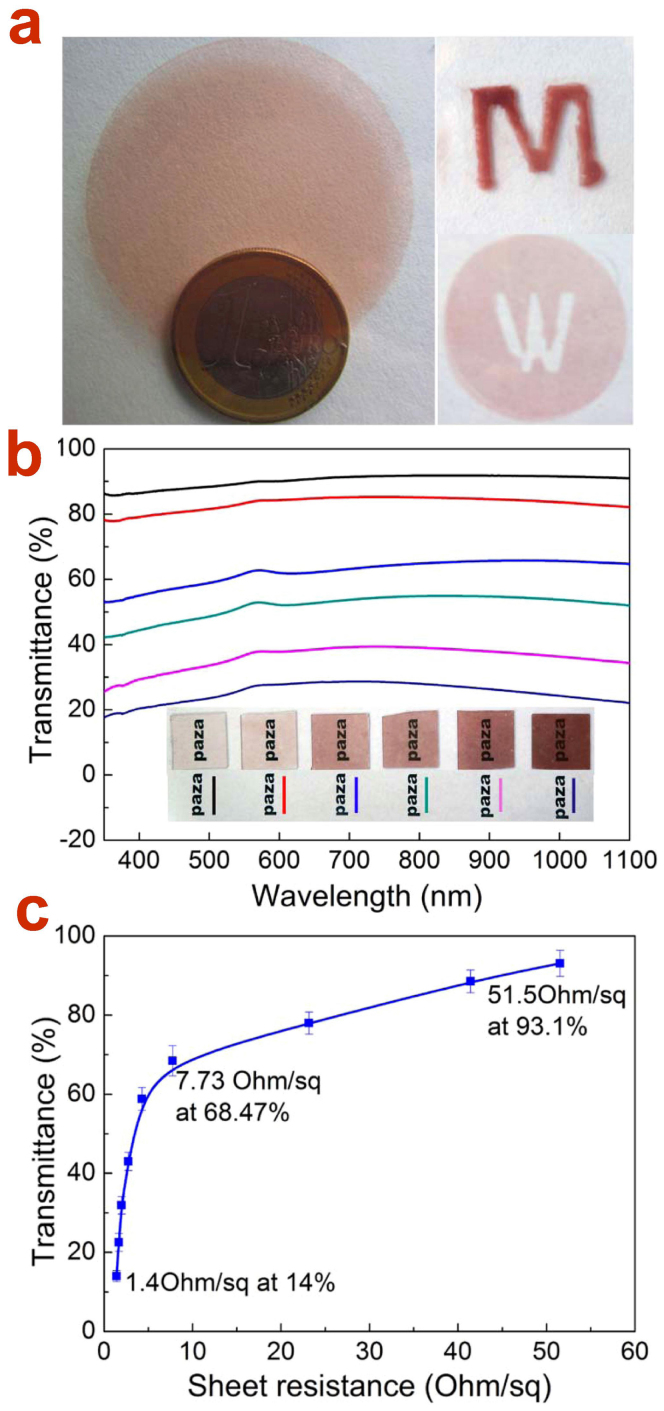
With these Cu NW “inks”, highly flexible, transparent and conductive thin films were prepared by percolation Cu NW nanoinks onto nitrocellulose membrane uniformly through vaccum suction. Then the percolation networks can be imprinted to any targeted substrates such as glass, Polyethylene terephthalate (PET), polyimide (PI), semiconductor wafer and etc., without any surface modification or bonding epoxy. Via this manner, selective area pattern and unlimited size can be easily achieved by the design of the filter and nitrocellulose membrane (Fig. 3a). The patterned Cu NW TEs are prepared by putting a mask on the membrane during vacuum filtration, as shown in the left panel of Fig. 3a. These as-transferred Cu TEs remain insulative due to the NW separation. Therefore, a thermal annealing at 100 ~ 200°C in vacuum oven is required to remove the surfactants and, more importantly, to accomplish the conductive network through nanowelding at the junctions between Cu NWs. By varying the concentration of Cu NW inks, a series of Cu NW network TEs in various thicknesses were prepared and their transmittances (Fig. 3b) and sheet resistances were measured. From Fig. 3b, one can see that the transmittance keeps nearly constant over the entire UV-Vis-NIR region and can be improved with decreasing the concentration of the Cu NW ink. This broad transparent windowof the Cu NW TE implies its wide application potential in optoelectronic devices covering from UV lighting to even infrared photovoltaic system4. The transmittance as a function of TE sheet resistance is plotted in Fig. 3c. One may see that the transparency of Cu TE increases steeply in the low resistance and then slowly gets saturated under higher resistance. The turning point appears at about 65% transmittance. It is found that the higher concentration Cu NW ink will lead to thicker NW networks and consequently results in lower sheet resistance (Fig. 3b and c). Specifically, Cu NWs TEs prepared in this work demonstrates an excellent optoelectronic performance (resistance versus transmittance): 1.4 Ohm/sq @ 14%, 2.2 Ohm/sq @ 32%, 2.9 Ohm/sq @ 43%, 4.6 Ohm/sq @ 58.6%, 7.73 Ohm/sq @ 68.47%, 23.3 Ohm/sq @ 78.1%, 41.6 Ohm/sq @ 88.8% and 51.5 Ohm/sq @ 93.1%. These results are comparable to (94.4% at 60 ohm/sq)20 or even overcome some of the TEs composed of Cu nanowires synthesized via solution route (90 Ohm/sq @ 90%)29, and including Cu nanofiber webs (50 Ohm/sq @ 90%)6 fabricated by electrospun as well.
Figure 3.
(a) Photographs of large scale and patterned Cu NW TEs imprinted on PET. This indicates that the unlimited size TEs in any desired pattern could be easily achieved though imprint technique. (b) UV-Vis-NIR transmission spectra for the Cu NW TEs fabricated with Cu NW inks in various concentrations (corresponding photographs in the inset). (c) Transmittance as a function of sheet resistance for Cu NWTEs, percolated with Cu NW inks in different concentrations.
Ohmic contact to active electronic materials
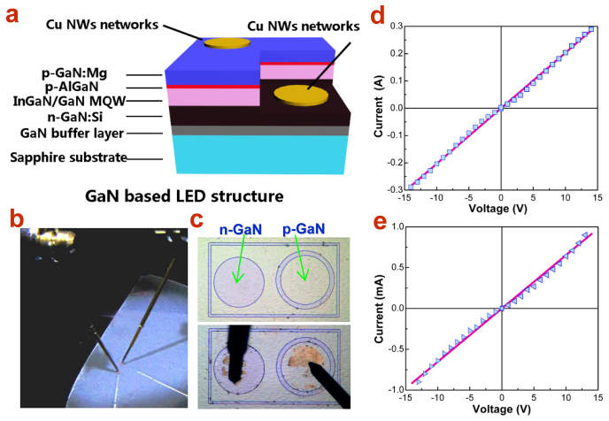
The Cu NW networks were applied as the TEs for GaN-based light emitting diodes (LEDs), in regard to its high conductivity and transmittance. The blue LED chips were fabricated by using metal-organic chemical vapor deposition (MOCVD) method. Fig. 4a displays the entire LED structure in a schematic cross-sectional view, consisting of the LED active layers and the contact of the Cu NW TEs to the p-type and n-type area. Although the Cu NW TE itself has embodied excellent performances, applications on optoelectronic devices would further require a high quality of contact with the semiconductor conducting layers, i.e., Ohmic contact. To improve the contact between the Cu NW TE and the GaN conducting layers, the 90%-transmittance Cu NW networks were imprinted onto the surface of p-GaN and n-GaNepilayers, respectively, as contact electrodes and the annealing temperature for nanowelding and contact was optimized. It is found that after annealing at 200°C for 1 h, the measured electrical I-V curves of these samples exhibit pretty good Ohmic type character over a wide voltage range, as shown in Fig. 4d and 4e. This approach may be also attributed to the nature of the ultra-long and super-fine shape of the Cu NWs, which are soft and flexible and may provide more contacting point with the beneath conducting layer. Therefore, even under a quite low annealing temperature compared to traditional NiAu electrodes, the Ohmic contact can be easily achieved.
Figure 4.
(a) Schematic illustration of the GaN-based LED structure together with Cu NW TEs on n- and p-type areas; (b) photograph of the setup of EL measurement of LED devices on a probe station; (c) optical micrographs of an individual LED unit before and after imprint of Cu NW TEs; (d) and e) I-V characteristics of the contact of Cu NW TEs to n-GaN and p-GaN, respectively. The Ohmic contact behavior is obtained with optimized annealing condition.
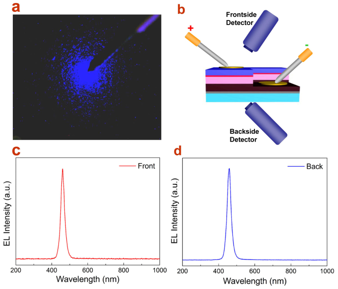
Based on the technique of Ohmic contact, the similar Cu NW TEs were imprinted through a designed pattern onto the etched n-type GaN and p-type GaN stage, respectively, in an individual LED chip (Fig. 4c). The picture of the measurement setup of electroluminescence (EL) on a probe stage is displayed in Fig. 4b. Figure 4c shows the Cu TE contacted p-type and n-type area with tip probes approached before applying input current. It can be seen that the Cu NW TEs have a high transmittance which may be significant for improving the light extraction from the LED active layers. When the input current is applied, as shown in Fig. 5a, bright blue light emits from the p-type injection area even at a low input current of about 100 μA. Most importantly, no dark area caused by light blocking is observed, which reflects the excellent transparency of the Cu NW TEs. In order to further confirm the effect of TE transparency, detecting fiber is set to collect the EL signal from the front face, where light will pass through the TE, or from the back face, where light comes out directly through the completely transparent sapphire substrate (Fig. 5b). As can be seen form Fig. 5c and d, the front-face EL spectrum has a comparable intensity with that of the back-face and meanwhile, no defect band relating with the TE contact is present. Thus, it is convinced that the Cu NW networks could be applied as excellent transparent electrode on advanced optoelectronic devices like LEDs.
Figure 5.
(a) Optical image of the blue light EL of InGaN-based LED with Cu NW TEs. The TE well transmits light without visible blocking. (b) Schematic of the detection setup for evaluation of the transparency of Cu NW TEs on LED device, with collection of EL spectra from the frontside and backside. (c) and (d) show the corresponding EL spectra, respectively.
Discussion
The absence of Ni in the products strongly suggests the catalytic role of Ni2+ ions during the Cu NW formation. To verify the catalytic role of Ni2+ ions and elucidate the reaction process, we designed two control experiments with different reaction solutions: one without any Ni2+ ions at all and the other with neutral Ni nanoparticles instead of Ni2+ ions. For the former case, it was found that no product was generated even by heating the solution up to 300°C. Because Cu2+ ions in Oleylamine solution were strongly coordinated by Cl−, which prevented they from being reduced. For comparison, Cu(NO3)2 was used as single precursor. As a result, Cu nanoparticles were generated after aging at 260°C for 60 min because of the absence of Cl− in the solution (see Supplementary Information for experimental details and Fig. S7). For the later, nickel nanoparticles (Fig. S8a) were synthesized in Oleylamine solution with 0.4 mmol Ni(acac)2 as precursor and dispersed in oleylamine solution containing 0.8 mmol CuCl2. After ageing at 175°C for 30 min (see Supplementary Information for experimental details), chaotic CuNi alloyed nanostructures (Fig. S8b and S9) were obtained and the rest Ni nanoparticles were dissolved in solution. This process can be explained by the oxidation of Ni(0) back to Ni2+ during the galvanic replacement reaction with Cu2+ ions. Thus, one can easily conclude that Ni2+ ions are necessary for the Cu NW synthesis as critical catalysts.
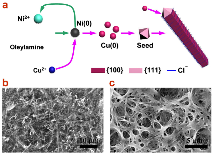
On the basis of above analysis, the formation process of Cu NWs is rather clear and can be described as follows, as shown in the schematic of Fig. 6a. Firstly, Ni2+ ions in Oleylamine solution will form Ni(0) atoms under heating. Secondly, Cu2+ ions involve into the galvanic replacement reaction with Ni(0) and the products Cu and Ni2+ come into being. The Ni2+ accomplishes its catalytic mission. Thirdly, dispersed Cu atoms begin to nucleate and form Cu nanocrystal seeds. In this stage, the NW is slowly growing. Fourthly, elongation of ultra-fine Cu NW is carried out with the presence of Cl− ions. The Cl− ions from CuCl2 precursor is indispensable because Cl− would attach onto the {100} facets and lead to a strongly anisotropic growth. In contrast, once Cu(CH3COO)2 was used to replace CuCl2 as copper precursor salts in the typical procedure, CuNi alloyed nanoparticles (see supporting information for experimental details and Fig. S10) instead of Cu NWs. This results in the rapid elongation along the [110] direction and the slow down growth rate on {100} facets, which restricts the diameter of Cu NWs. By well control of the reaction temperature, the ultra-long and fine Cu NWs can be successfully synthesized, overcoming the limit of the aspect ratio on metal nanowires. To further confirm this mechanism, we introduced Ni2+ by replacing the precursor Ni(acac)2 with Ni(OAc)2 or Ni(NO3)2, without other changes from the typical procedure. Figure 6b and c display the SEM images of Cu NWs synthesized with Ni(OAc)2 and Ni(NO3)2 as catalysts, respectively. Representative EDS spectra and XRD pattern of the Cu NWs synthesis with Ni(ac)2 as catalyst are shown in Fig. S8. These results well indicate that this Ni2+-catalyst mechanism could be valid for any Ni2+-containing salts as catalyst to generate Cu NWs.
Figure 6.
(a) Schematic of the formation mechanism of Cu NWs. The Ni2+ and Cl− ions play critical roles in promoting the growth of high aspect ratio Cu NW. (b) and (c), SEM images of Cu NWs synthesized with Ni(OAc)2 and Ni(NO3)2 as precursors, respectively, which confirm the catalytic effect with the presence of Ni2+ ions.
Obviously, this outstanding performance in Cu NW electrodes is mainly attributed to their geometric features and way of network connecting: super length, small diameter, particle free, and firm welding. i), the super length of Cu NWs plays the dominant role in forming excellent conductivity. As aforementioned, the percolation theory for one-dimensional wires Nth = (4.236/L)2/π shows that conductivity of a nanowire network can be largely enhanced with the elongation of the nanowires. If we look the free electron as a car, then the nanowires could be the single-lane highway. Once the car is driven onto a super-long highway, it can just keep at a constant high speed for a long distance without frequently slowing down and changing at the crossing. This is the reason why the good conductivity of Cu NW TE could be achieved even with a low Cu NW concentration (Fig. 7a). ii), the small diameter pushes the transparency and flexibility. When the Cu NWs are made into networks, the fine NWs provides wider spacing which allows light to pass through. On the other hand, the small diameter makes the Cu NW soft enough to bend in any shape without being broken. In addition, the nanowelding temperature to form a relatively strong welding spot between two Cu NWs can be lowered due to the small contact volume. iii), particle free on the Cu NW surface could reduce the surface conductivity and iv), firm welding of connection point between NWs is attributed to the low nanowelding temperature (100 ~ 200°C). The last point will be further revealed below.
Figure 7.
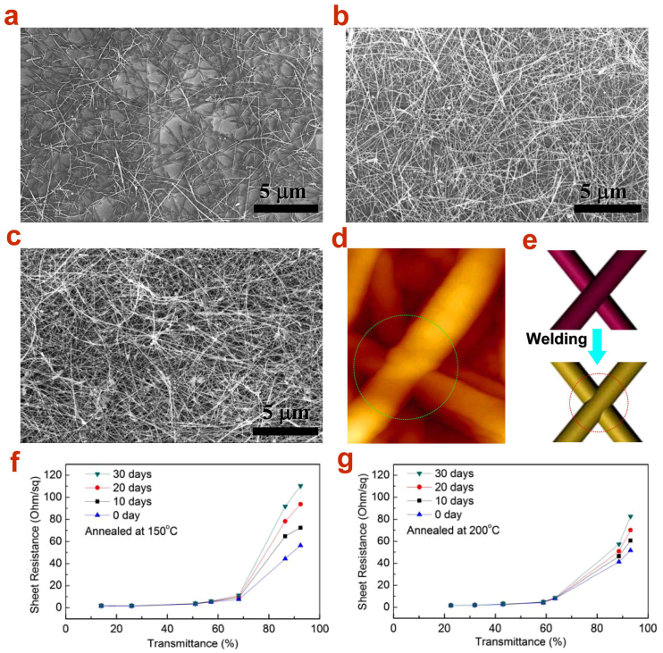
(a–c) SEM images of the Cu NW TEs on glass substrates with a transmittance at 87%, 62.8% and 32.8%, respectively. (d) AFM image of Cu NW after annealing at 200°C for 1 h, where the welding point has been formed, and (e) schematic of the nanowelding between two NWs before and after annealing. (f) and (g) Transmittance vs. sheet resistance for the Cu NW TEs which were annealed at 150°C and 200°C, respectively, and exposed in air for 30 days. Annealing at 200°C can significantly improve the stability of Cu NW TEs.
Fig. 7a–c display the SEM images of the Cu NW TEs on glass substrates with a transmittance at 87%, 62.8%, 32.8%, respectively, after annealed at 200°C in a vacuum oven for 1 h. Clearly, the Cu NWs remain interconnected and continuous, and no aggregation or fracture is observed. The AFM image in Fig. 7d shows the connecting point between two crossing Cu NWs after annealing treatment, which has been fused together. As schematically demonstrated in Fig. 7e, the toughing point after thermal annealing process will eat each other and form a firm thermo welding junction that becomes conducting. The Cu TEs have been subjected to mechanical bending and stretching by 180° for 100 times and finally, the conductivity is still well preserved (Fig. S11).
It has been well known that copper will be oxidized by oxygen in the air. In this regard, a series of aging experiments were carried out on these Cu NW TEs to characterize their stability. Two groups of control samples of Cu NW networks were prepared and annealed under 150°C and 200°C, respectively, for 1 h. Then they were exposed in the air for 30 days and the sheet resistance and transmittance was measured every 10 days. Fig. 7f shows the results for the group annealed at 150°C. It can be seen clearly that the transmittance of TEs remains unchanged and the sheet resistances of samples with a transmittance below 60% appears rather stable. Whereas, for the samples with higher transmittance (>60%), the resistance begins to increase and becomes 120 Ohm/sq for the 93% sample after 30 days. This aging effect reflects that the influence by the oxidation of Cu would be significant for the sample with incompact NWs (high transparency). Actually, it is the formation of oxides such as CuO at the surface of the welding spot which deteriorates the conductivity of the contact point. The more compact Cu NWs network processes a more excellent oxidation-resistant ability. In contrast, this problem has been largely improved for the group annealed at 200°C, as shown in Fig. 7g. Although the resistance still has a tendency of increasing as a function of aging time, the increment for the 93%-transmittance sample is only about 31 Ohm/sq from 51.5 Ohm/sq to 82.6 Ohm/sq after exposure for 1 month. This means that the higher annealing temperature will make a more firm welding junction with less active Cu surface, which might lead to a higher oxidation resistance for the Cu NW TEs. Sheet resistances of the samples annealed at 100°C were fluctuant versus the transmittance after exposed in the air for a couple days (Fig. S12). It may result from the unstable junctions between Cu NWs. The welding junctions were formed basing on a diffusion process between a couple Cu NWs touching with each other, which were highly sensitive to oxidation damage compared to the body of Cu NWs. Therefore, the oxidation on the welding junction would play a vital role in affecting the Cu NW stability. Work along this line with temperature optimization and oxidation-resistant coating is still in process.
In summary, highly dispersed Cu NWs possessing a long (entire length up to 40 μm) and fine (average diameter of 16.2 ± 2 nm) geometric nature have been successfully synthesized through nickel ion catalytic process. A series of experiments were carried out to clarify the critical mechanism of the newly developed catalytic scheme, which demonstrates that active Ni2+ and Cl− ions play a key role in pushing the stable NW elongation and meanwhile restricting the lateral diameter. Such nanowire geometry is crucial for overcoming the limit of transparency and conductivity of metal nanowire TEs. As a result, the Cu NW TEs showed a significantly superior conductivity (1.4 Ohm/sq) and transmittance (93% @ 51 Ohm/sq) over a broad band from ultraviolet to infrared. Furthermore, the Cu NW ink could be unrestrictedly percolated onto filter membrane in any size and with any desired pattern, and then transferred onto various substrates to form TEs. As an example, application of Cu NWs as contact electrodes was made on GaN-based blue LED units. Ohmic contact to n- and p-type GaN was easily formed with low temperature annealing (200°C) and the bright EL was achieved showing the excellent transparency. In virtue of the superior properties, low cost and capability of mass synthesis, further improvement of the performance stability is believed to lead to a replacement of traditional ITO in the near future.
Methods
Chemicals
Copper(II) chloride dihydrate (CuCl2·H2O, AR, SCRC), Nickel(II) acetylacetone (Ni(acac)2, 95%, Strem Chemicals Inc.), nickel(II) acetate tetrahydrate (Ni(ac)2·4H2O, AR, SCRC), nickel(II) nitrate (Ni(NO3)2·6H2O, AR, SCRC), hexane (AR, SCRC), toluene (AR, SCRC), trichloromethane (CHCl3, AR, SCRC) and oleylamine (80 ~ 90%, Acros Organics) were all used as received.
Preparation of Cu NWs
In a typical procedure, 0.8 mmol CuCl2·H2O and 0.4 mmol Ni(acac)2 were mixed with 10 ml oleylamine in a 50 ml three-necked flask and kept under a flow of high-purity argon at 80°C for 20 min with strong magnetic stirring. After fully dissolution, the resulting solution was heated up to 175°C and kept at this temperature for 10 h. After cooling down to room temperature naturally, excess hexane was added into the red solution to give a red precipitate which was isolated via centrifugation (10000 rpm for 10 min). Cu NWs ink was obtained by washing the precipitate with a mixture of hexane and acetone, and then dispersing them into hexane by bath sonication for 10 min. Equivalent mole C4H6O4Ni·4H2O/Ni(NO3)2·6H2O instead of Ni(acac)2 was used to catalytic synthesis of Cu NWs following the same procedure mentioned above.
Fabrication of transparent conductive films from the Cu NWs ink
Thin films were percolated by vacuum filtration and transfer to substrate. Typically, Cu NWs ink was filtered onto a nitrocellulose membrane uniformly by vacuum suction to form Cu NWs percolation network. Afterward, the nitrocellulose membrane which contact intimately with Cu NWs was put onto targeted substrate flat. Then the nitrocellulose membrane was peeled off to leave Cu NWs network on the substrate after applying a uniform pressure on the other side of membrane for 30 seconds. The thin films can also be patterned easily by putting a mask on the membrane during the vacuum filtration. Finally, a subsequent thermal annealing aiming for surface surfactant removing and nanowelding among Cu NWs was applied in a vacuum oven at 200°C for 1 hour.
Fabrication of LED devices with Cu NWs transparent electrodes
The GaN-based LED epitaxy-layers were grown on a c-plane sapphire substrate by metal-organic chemical vapor deposition (MOCVD). A 2.9 μm thick undopedGaN layer and 4 μm thick n-GaN:Si layer were grown at 1020°C on sapphire substrate before the growth of three InGaN(3 nm)/GaN(10 nm) multiple quantum wells (MQWs) at 770°C, and this was followed by the growth of 3 nm p-AlGaN. Then, a 200 nm thick p-GaN:Mg layer were grown at 950°C. After that, the epitaxy layers were etched by an inductively coupled plasma (ICP) etching process using Cl2/CH4/H2/Ar source gases in the presence of protective photoresist as an etch mask until the n-GaN layer was exposed. To form Cu NWs networks as transparent electrodes for Ohmic contact to GaN-based LED, anitrocellulose membrane covered with Cu NWs networks was flattened upon the GaN-based LED, then a a uniform pressure was applied on the p-typed and n-typed areas from the opposited side to transfer the Cu NW networks to the trageted areas, respectively. Finally, annealing treatment aiming for surfactant removing, nanowelding and interfacial modification was carried out at 200°C in a vacuum oven for 1 hour. For the ohmic contact test, Cu NWs networks were transferred onto the surface of p-GaN or n-GaN by the same process.
Characterization
The as-obtained Cu NWs and electrodes were characterized by means of X-ray diffraction measurements (Panalytical X'pert PRO diffractometer using Cu Kα radiation, operating at 40 kV and 30 mA), scanning electron microscope (LEO S-4800 scanning electron microscope operated at 20 kV) and transmission electron microscope (TECNAI F-30 transmission electron microscope operated at 300 kV). The transmttance was tested on a Shimadzu UV-2550 ultraviolet-visible-near-infrared spectrophotometer. The sheet resistance was measured using a four-wire resistivity measure with a Keithley 2400 measurement system at room temperature. The current-voltage (I-V) characteristics measurement was carried out on a probe station with a Keithley617 system and an optical microscope for electroluminescene microscopic images taking. Atomic force microscope (AFM) characterization was carried out using a Scan Asyst-Air (Bruker Multimode 8, Bruker ASX Inc., Madison, WI, USA). Measurements were carried out in air using non-contact AFM mode.
Author Contributions
H.G., D.C., D.P. and Y.C. designed the research and co-wrote the paper. H.G., D.C., N.L., Z.W. and Q.X. performed the experiment and analysis the data. T.Z., N.G., S.L. and J.K. fabricated the GaN LED.
Supplementary Material
Copper Nanowires as Fully Transparent Conductive Electrodes
Acknowledgments
The authors gratefully acknowledge financial support from the National Basic Research Program of China (no. 2012CB933103), the National Outstanding Youth Science Foundation of China (grant no. 50825101), the “973” programs (2012CB619301 and 2011CB925600) and “863” (2011AA03A111), the FRFCU (2012121011 and 2011121042), the National Natural Science Foundation (51171158, 61204101, 61227009, and 90921002).
References
- Katayama M. TFT-LCD technology. Thin Solid Films 341, 140–147 (1999). [Google Scholar]
- Liu H. Y., Avrutin V., Izyumskaya N., Ozgur U. & Morkoc H. Transparent conducting oxides for electrode applications in light emitting and absorbing devices. Superlattice Microst. 48, 458–484 (2010). [Google Scholar]
- Gomez De Arco L. et al. Continuous, Highly Flexible, and Transparent Graphene Films by Chemical Vapor Deposition for Organic Photovoltaics. ACS Nano 4, 2865–2873 (2010). [DOI] [PubMed] [Google Scholar]
- Granqvist C. G. Transparent conductors as solar energy materials: A panoramic review. Sol. Energ. Mat. Sol. C. 91, 1529–1598 (2007). [Google Scholar]
- Kang M. G. & Guo L. J. J. Vac. Sci. Technol. B 25, 2637–2641 (AVS). [Google Scholar]
- Wu H. et al. Electrospun Metal Nanofiber Webs as High-Performance Transparent Electrode. Nano Lett. 10, 4242–4248 (2010). [DOI] [PubMed] [Google Scholar]
- Betz U., Kharrazi Olsson M., Marthy J., Escolá M. F. & Atamny F. Thin films engineering of indium tin oxide: Large area flat panel displays application. Surf. Coat. Tech. 200, 5751–5759 (2006). [Google Scholar]
- Leterrier Y. et al. Mechanical integrity of transparent conductive oxide films for flexible polymer-based displays. Thin Solid Films 460, 156–166 (2004). [Google Scholar]
- Doherty E. M. et al. The spatial uniformity and electromechanical stability of transparent, conductive films of single walled nanotubes. Carbon 47, 2466–2473 (2009). [Google Scholar]
- Bae S. et al. Roll-to-roll production of 30-inch graphene films for transparent electrodes. Nat. Nanotechnol. 5, 574–578 (2010). [DOI] [PubMed] [Google Scholar]
- Reina A. et al. Large Area, Few-Layer Graphene Films on Arbitrary Substrates by Chemical Vapor Deposition. Nano Lett. 9, 30–35 (2008). [DOI] [PubMed] [Google Scholar]
- Kim U. J. et al. Graphene/Carbon Nanotube Hybrid-Based Transparent 2D Optical Array. Adv. Mater. 23, 3809–3814 (2011). [DOI] [PubMed] [Google Scholar]
- Ahn S. H. & Guo L. J. Large-Area Roll-to-Roll and Roll-to-Plate Nanoimprint Lithography: A Step toward High-Throughput Application of Continuous Nanoimprinting. ACS Nano 3, 2304–2310 (2009). [DOI] [PubMed] [Google Scholar]
- Ahn S. H. & Guo L. J. Spontaneous Formation of Periodic Nanostructures by Localized Dynamic Wrinkling. Nano Lett. 10, 4228–4234 (2010). [DOI] [PubMed] [Google Scholar]
- Lee J.-Y., Connor S. T., Cui Y. & Peumans P. Solution-Processed Metal Nanowire Mesh Transparent Electrodes. Nano Lett. 8, 689–692 (2008). [DOI] [PubMed] [Google Scholar]
- Scardaci V., Coull R., Lyons P. E., Rickard D. & Coleman J. N. Spray Deposition of Highly Transparent, Low-Resistance Networks of Silver Nanowires over Large Areas. Small 7, 2621–2628 (2011). [DOI] [PubMed] [Google Scholar]
- Leem D.-S. et al. Efficient Organic Solar Cells with Solution-Processed Silver Nanowire Electrodes. Adv. Mater. 23, 4371–4375 (2011). [DOI] [PubMed] [Google Scholar]
- Hu L., Kim H. S., Lee J.-Y., Peumans P. & Cui Y. Scalable Coating and Properties of Transparent, Flexible, Silver Nanowire Electrodes. ACS Nano 4 (2010). [DOI] [PubMed] [Google Scholar]
- Rathmell A. R., Bergin S. M., Hua Y.-L., Li Z.-Y. & Wiley B. J. The Growth Mechanism of Copper Nanowires and Their Properties in Flexible, Transparent Conducting Films. Adv. Materi. 22 (2010). [DOI] [PubMed] [Google Scholar]
- Rathmell A. R., Nguyen M., Chi M. & Wiley B. J. Synthesis of Oxidation-Resistant Cupronickel Nanowires for Transparent Conducting Nanowire Networks. Nano Lett. 12, 3193–3199 (2012). [DOI] [PubMed] [Google Scholar]
- Hsu P.-C. et al. Passivation Coating on Electrospun Copper Nanofibers for Stable Transparent Electrodes. ACS Nano 6, 5150–5156 (2012). [DOI] [PubMed] [Google Scholar]
- Wu H. et al. A transparent electrode based on a metal nanotrough network. Nat Nano 8, 421–425 (2013). [DOI] [PubMed] [Google Scholar]
- Hu L., Wu H. & Cui Y. Metal nanogrids, nanowires, and nanofibers for transparent electrodes. MRS Bulletin 36, 760–765 (2011). [Google Scholar]
- Lee P. et al. Highly Stretchable and Highly Conductive Metal Electrode by Very Long Metal Nanowire Percolation Network. Adv. Mater. 24, 3326–3332 (2012). [DOI] [PubMed] [Google Scholar]
- Jin M. et al. Shape-Controlled Synthesis of Copper Nanocrystals in an Aqueous Solution with Glucose as a Reducing Agent and Hexadecylamine as a Capping Agent. Angew. Chem. Int. Edit. 50, 10560–10564 (2011). [DOI] [PubMed] [Google Scholar]
- Guo H., Chen Y., Ping H., Jin J. & Peng D.-L. Facile synthesis of Cu and Cu@Cu-Ni nanocubes and nanowires in hydrophobic solution in the presence of nickel and chloride ions. Nanoscale 5, 2394–2402 (2013). [DOI] [PubMed] [Google Scholar]
- Ellmer K. Past achievements and future challenges in the development of optically transparent electrodes. Nat. Photon. 6, 809–817 (2012). [Google Scholar]
- Ye E., Zhang S.-Y., Liu S. & Han M.-Y. Disproportionation for Growing Copper Nanowires and their Controlled Self-Assembly Facilitated by Ligand Exchange. Chem. A Eur. J. 17, 3074–3077 (2011). [DOI] [PubMed] [Google Scholar]
- Zhang D. et al. Synthesis of Ultralong Copper Nanowires for High-Performance Transparent Electrodes. J. Am. Chem. Soc. 134, 14283–14286 (2012). [DOI] [PubMed] [Google Scholar]
- Huang X. & Zheng N. One-Pot, High-Yield Synthesis of 5-Fold Twinned Pd Nanowires and Nanorods. J. Am. Chem. Soc. 131, 4602–4603 (2009). [DOI] [PubMed] [Google Scholar]
- Lu L., Shen Y., Chen X., Qian L. & Lu K. Ultrahigh Strength and High Electrical Conductivity in Copper. Science 304, 422–426 (2004). [DOI] [PubMed] [Google Scholar]
- Guo H., Chen Y., Ping H., Wang L. & Peng D.-L. One-pot synthesis of hexagonal and triangular nickel-copper alloy nanoplates and their magnetic and catalytic properties. J. Mater. Chem. 22, 8336–8344 (2012). [Google Scholar]
- Atwater H. A. & Polman A. Plasmonics for improved photovoltaic devices. Nat. Mater. 9, 205–213 (2010). [DOI] [PubMed] [Google Scholar]
- Jeong S. et al. Controlling the Thickness of the Surface Oxide Layer on Cu Nanoparticles for the Fabrication of Conductive Structures by Ink-Jet Printing. Adv. Funct. Mater. 18, 679–686 (2008). [Google Scholar]
Associated Data
This section collects any data citations, data availability statements, or supplementary materials included in this article.
Supplementary Materials
Copper Nanowires as Fully Transparent Conductive Electrodes


