Abstract
Surface-enhanced Raman scattering (SERS) is attracting increasing interest for chemical sensing, surface science research and as an intriguing challenge in nanoscale plasmonic engineering. Several studies have shown that SERS intensities are increased when metal island film substrates are excited through a transparent base material, rather than directly through air. However, to our knowledge, the origin of this additional enhancement has never been satisfactorily explained. In this paper, finite difference time domain modeling is presented to show that the electric field intensity at the dielectric interface between metal particles is higher for “far-side” excitation than “near-side”. This is reasonably consistent with the observed enhancement for silver islands on SiO2. The modeling results are supported by a simple analytical model based on Fresnel reflection at the interface, which suggests that the additional SERS signal is caused by near-field enhancement of the electric field due to the phase shift at the dielectric interface.
Surface-enhanced Raman scattering (SERS) provides a sensitive method for detecting trace levels of a wide range of chemical and bio-chemical compounds adsorbed on nanostructured plasmonic metal surfaces1,2,3. The most commonly used metals include silver, gold and copper4. The process is related to normal Raman scattering, where a small fraction of incident laser light is inelastically scattered by molecular vibrational modes of the target molecule, producing a ‘signature' spectrum of the chemical compound. SERS boosts the typical Raman scattering cross section by a factor of 106 or more5,6.
The enhancement arises primarily from the enhanced electromagnetic field (EM mechanism) produced by resonant excitation of the surface electrons in the metal nanostructures by laser light7. This EM mechanism can be used to explain several facets of SERS including the distance dependence, metal specificity, nanoparticle shape and size dependence and the generation of SERS ‘hot spots'7,8,9,10. Computer-based modeling of the EM mechanism not only provides a quantification of the effect but can also guide efforts to engineer the surface geometry in order to maximize the signal yield6. In addition to the EM mechanism there is also a sample dependent “chemical” enhancement mechanism that may arise due to charge transfer interactions with the metal11. A further enhancement can be generated by excitation of a higher electronic state of the molecule, referred to as surface-enhanced resonance Raman scattering (SERRS). A unified description of these various factors has been proposed in terms of Herzberg-Teller vibronic coupling12.
A number of different methods have been employed for the fabrication of nanostructured metal surfaces suitable for SERS13. In many cases, metal particles are deposited on a dielectric substrate, which is typically glass. Traditionally, the resulting SERS substrate is then excited from the “air” side in a backscattering geometry. Efforts to identify alternative measurement geometries have led to several reports that a larger SERS signal is obtained by excitation through the dielectric medium than by excitation through air14,15,16,17,18. Jennings et al.14 reported the use of glass slides with vacuum deposited silver/indium island films and a 90° scattering geometry. They did not quantify the extra enhancement, but suggested a ‘first layer effect', where the analyte layer that is closest to the enhancement field generates a higher signal. However, this argument appears to have fallen out of favour in later work where the extra enhancement was observed for monolayer adsorbates15. Bello et al. excited a silver-coated titanium dioxide nanoparticle substrate in the far-side illumination at a 90° scattering geometry and reported the observation of a SERS signal that was 11 times higher than in the direct illumination16. A similar behavior was observed by the same group again using silver-coated microspheres17. In the absence of a convincing mechanism or explanation via current theoretical accounts18, this additional enhancement appears to have been relatively neglected since then.
A better understanding of the far-side excitation is particularly important for remote sensing applications of SERS where the laser light is coupled through an optical fibre to excite the sensing element either at the distal end or along the cylindrical surface19,20. In this case the higher than expected signal could be exploited to produce a more sensitive detector.
The work presented here demonstrates the extra enhancement in the far-side excitation geometry using SERS substrates fabricated by oblique angle deposition (OAD)20,21 on glass cover slips with a refractive index of 1.47. It is shown that these substrates exhibit an enhancement that is approximately three times higher than the direct illumination. This observation is supported by finite-difference time-domain (FDTD) modeling of the plasmon behavior at the dielectric boundary between pairs of hemispherical nanoparticles. Further analysis of Fresnel reflection and transmission terms suggests a simple physical explanation of this phenomenon based on the phase shift of light at the dielectric-air interface.
Results
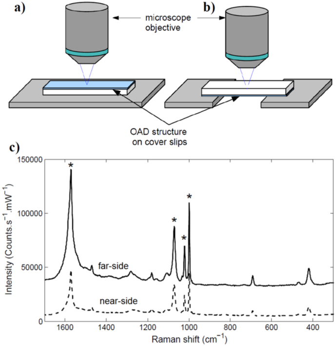
In order to investigate the SERS response in the near- and far-side excitation geometries, the arrangements shown in Fig. 1(a) and (b) were used. In both geometries the microscope objective was focused on the surface which contained the silver island film. Typical thiophenol SERS spectra are shown in Fig. 1(c) for near- and far-side excitation with a 5 × objective. The measurements were taken using several different microscope objectives, which provided a range of collection apertures as listed in Table 1.
Figure 1. Cover slips coated with silver using OAD and measured for SERS in (a) near-side interrogation and (b) far-side interrogation with (c) the resulting thiophenol SERS spectra taken from an OAD substrate of 100 nm nominal thickness with a 5 × objective.
The spectra have been vertically offset for clarity. An average intensity value was obtained for each spectrum from the four main thiophenol peaks, denoted by *.
Table 1. The numerical aperture and solid angle of light collection for different microscope objectives.
| Objective | Numerical Aperture (NA) | Solid Angle Ω (sr) |
|---|---|---|
| 5 × | 0.12 | 0.045 |
| 10 × | 0.25 | 0.200 |
| 20 × | 0.4 | 0.525 |
| 50 × | 0.5 | 0.842 |
| 50 × | 0.75 | 2.13 |
| 100 × | 0.85 | 2.97 |
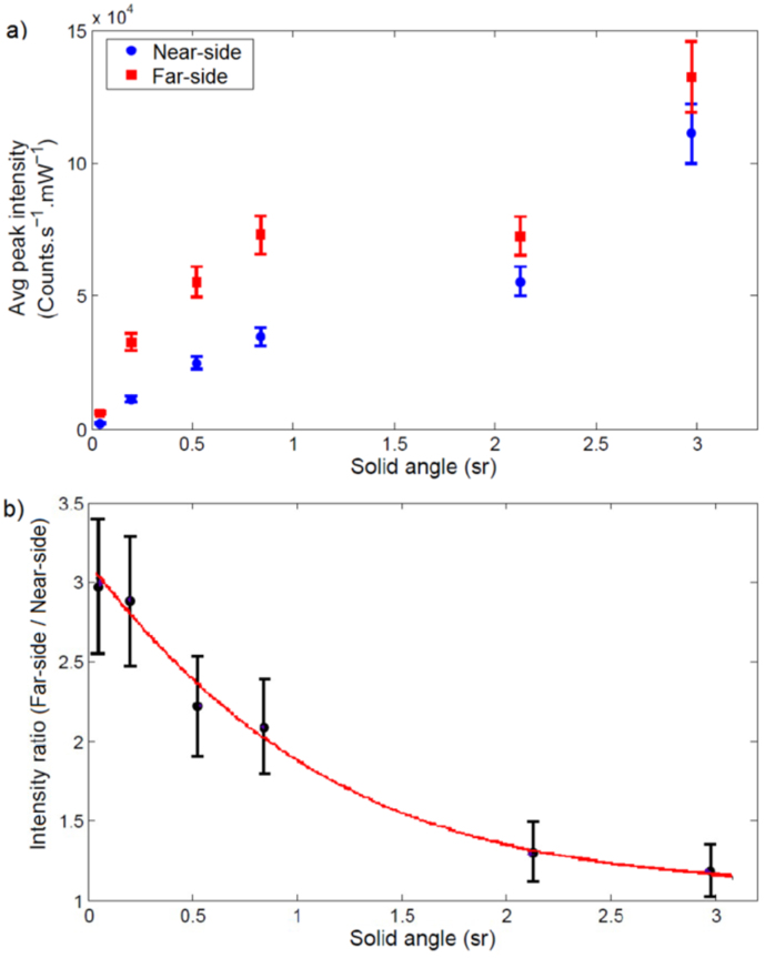
The average SERS intensity values for near- and far-side interrogation at five different positions on three different substrates are plotted against the solid angle of signal collection in Fig. 2(a). It is interesting to note that the average peak intensity does not increase linearly with solid angle, as would be expected for isotropic scattering. However, the far-side intensity is consistently higher than the near-side across all objectives, as shown by the ratio between the average peak intensities in Fig. 2(b). For the low NA objectives this ratio is approximately 3 and it decreases for higher NA objectives. Possible reasons for the behavior shown in these graphs will be explored in the following theoretical analysis. Note that it is justified to use the average peak intensity as a proportional measure of average enhancement in this case, as the solid angle dependence of each of the four individual peaks is the same within experimental error.
Figure 2.
(a) Average peak intensity of the four main thiophenol peaks acquired using different microscope objectives. The substrates were fabricated using OAD on glass cover slips with a 100 nm nominal silver deposition thickness. (b) The ratio between far-side and near-side measurements taken from the same SERS substrate for a range of microscope objectives. The smoothing spline fit is included as a guide to the eye.
FDTD modeling
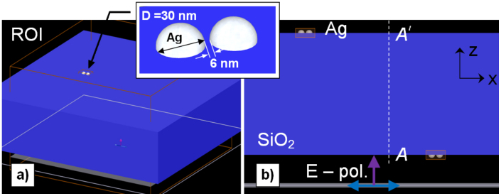
In order to understand the additional enhancement observed in the far-side geometry, a 3D-finite-difference time-domain (FDTD) simulation was carried out with the FDTD Solutions software (Lumerical Solutions, Inc.). The silver islands that formed the SERS substrates in these experiments were approximated as hemispherical silver nanoparticles of 30 nm diameter and 15 nm height. These dimensions were based on SEM analysis of the substrates, with a typical image shown in Fig. 3. The simulation was used to evaluate the field intensities produced in nanogaps of 6 nm between hemispherical particles, as shown in Fig. 4(a). A SiO2 slab of 1 μm thickness was positioned inside the modeling domain and the nanoparticles were placed in two pairs: one on the slab side closest to the light source (near-side) and one on the opposite (far) side. The pairs are spaced by 1 μm along the x-axis, which is enough to gather data on both pairs in the same simulation without mutual interference. The domain size is 1 × 1 × 2 μm3, illuminated by an x-polarized plane wave light source with bandwidth from 350 to 650 nm wavelength. Periodic boundary conditions are placed on the x- and y-boundaries to avoid plane wave diffraction at the domain edges. The silver and silica materials are modeled in the Lumerical database by time-domain polynomial fitting of the tabulated experimental (n, k) spectra according to Palik22.
Figure 3. A scanning electron microscope (SEM) image of silver nanoislands, fabricated by oblique angle deposition with a nominal thickness of 100 nm.
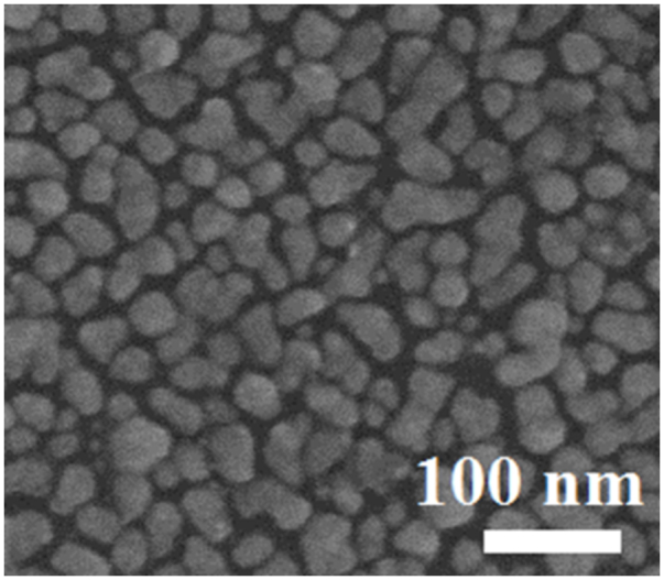
Figure 4. FDTD modeling domain (region of interest - ROI) comprising a silica slab of 1 μm thickness (in blue) and two pairs of hemispherical silver nanoparticles, positioned at 1 μm spacing on the near side (x-positive) and far side (x-negative) with respect to the x-polarized plane wave source (white square).
Projections are shown for (a) 3D perspective, (b) xz-plane. Inset in (a): a detail of the nanoparticle pair is shown, the sphere diameter is 30 nm, and the nanogap width is 6 nm. The A–A′ cross section was used to estimate the field distribution at the dielectric boundary.
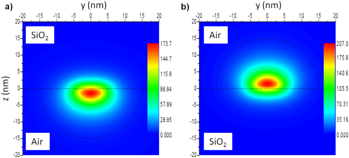
A single broadband field enhancement peak was found at 440 nm wavelength, where hot spots appeared in the middle of the nanogap at the interface between silica and air. The resonance wavelength was found to be influenced by the thickness of the silica slab, but it did not have a significant effect on the resultant fields. As the excitation wavelength was 514.5 nm and the emission wavelength was 548 nm, in Fig. 5 the electric field intensity distribution (E2) is shown close to the excitation wavelength, on matching yz-parallel planes bisecting the nanogaps on the respective sides. On the near side, the field intensity enhancement on the glass surface (normalized to source intensity) peaks at 136, while on the far side it peaks at 162. The same values for the emission wavelength are 43 and 78, respectively. The SERS signal is approximately proportional to the square of the electric field at the excitation wavelength multiplied by the square of the electric field at the emission wavelength1,23. Therefore the ratio of the SERS signals arising from this hot spot is given by (Efar,ex/Enear,ex)2(Efar,em/Enear,em)2 ~ 2.16. While this differs somewhat from the experimental value of 3 found for the smallest collection aperture in the previous section, it does suggest that an increase in the electric field could be driving increased SERS emission.
Figure 5. Electric field intensity distribution (values normalized to plane wave source intensity) at 510 nm wavelength on a yz-parallel plane cutting across the center of the nanogap between the two particles on (a) near side and (b) far side.
The dashed lines depict the air-glass interface and the silver nanoparticle outline projection on the yz-plane. The hot spot maximum is located slightly above the interface in the middle of the nanogap.
The use of a finite collection aperture is not exactly comparable to the plane wave case, but is unavoidable in this experimental set-up as the signal tends to zero as the collection aperture tends to zero (see Fig. 1(a)). Note that there is considerable evidence that the SERS signal tends to be dominated by scattering from hot spots such as the nanogap considered in this model24,25. Recent FDTD modeling has confirmed that this assumption remains valid for the case of silver island films formed by oblique island deposition10.
In order to investigate whether the higher field intensity for far-side enhancement was due to a purely geometrical effect, a further simulation was performed where the Ag hemispheres were inverted relative to the glass surface. This left the hemispheres contacting the glass at a point in the centre of the curved surface. Although this arrangement is not directly relevant to the experimentally achieved structures, it serves to separate the influence of the dielectric interface from possible shape and orientation effects in the metal particles. In this case the simulation again indicates that the far-side field intensity is approximately twice as large as the near-side intensity. Therefore the effect does not rely on the orientation of the particle with respect to the direction of incidence of the light. However, the peak field intensity is associated with the points where the gap between the particles is smallest, which is now approximately 15 nm above the silica surface. Nevertheless, a comparison of the field intensities at the contact points of the metal on the silica surface shows the same ratio of two between far- and near-side excitation.
In order to separate the effect of the plasmon field enhancement from the field distribution at the dielectric boundary, the fields were also evaluated at the dielectric boundary along the cross section A–A′ in Fig. 4(b). The simulations at the excitation wavelength show that E2 = 0.64 in front of the entrance surface at point A and E2 = 0.82 at the exit point A′, which corresponds to a field intensity ratio of 1.28. The same values for the emission wavelength are 0.53 and 0.86, respectively. Hence the expected far-side SERS enhancement would be (EA′,ex/EA,ex)2 (EA′,em/EA,em)2 ~ 2.1. Further simulations were performed for cases in which the hemispherical nanoparticles were raised by a certain distance above the silica surface. The enhancement recorded at the surface is reduced by one order of magnitude for every 5 nm of separation between surface and particles, and the ratio between the field intensities stabilizes at 1.28 for distances of 15 nm or more.
Given that the additional field enhancement for far-side excitation appears to be reasonably consistent, regardless of the particular arrangement of the Ag particles, it is postulated that the effect is associated with the nearby dielectric boundary. The nature of this boundary is discussed in the following Section.
Fresnel mechanism
According to the Fresnel formulae for right angle incidence (θi = 0), the coefficients of the in-plane (∥) polarized amplitudes of transmitted and reflected electric fields are, respectively26:
where ni and nt are the refractive indices of the materials on the incidence and transmission sides, respectively. The field component perpendicular to the plane of incidence is  and
and  , while the corresponding intensities are r2 and t2. The Fresnel equations suggest that an E-field enhancement occurs when light passes from the medium with a larger refractive index to the medium with lower refractive index. In the case of a glass-air boundary (ni = 1.5, nt = 1) the transmitted field is enhanced by a factor of t = (3/2.5) = 1.2, while for an air-glass boundary there is a loss in transmission t = (2/2.5) = 0.8 when the incident field is |E| = 1. Hence, a 20% gain at the exit interface can be obtained for the light passing through the glass plate. The physical basis for this enhancement is the phase shift that occurs at the boundary.
The energy (intensity) conservation condition T + R = 1 is fulfilled in the far-field as (nt/ni)t2 + r2 = 1. This is illustrated in Figs. 6(a) and (b) and is irrespective of the direction of light propagation: from high-to-low index material or vice versa. The strong enhancement of the E-field that occurs at the interface when light traverses from a high index to low index medium is shown in Fig. 6(d). The far-field conservation of energy (intensity) does not forbid a significant local E-field enhancement in this case. In the SERS experiments this situation corresponds to the far-side excitation (through the sample). From this argument it would appear that an additional SERS enhancement of E4 ~ t4 = 2.01 is achievable on the far-side surface of silica substrates (n = 1.47) patterned with plasmonic nanostructures. For the realistic experimental situation, reflection losses through the slab should also be considered. If the air on the near-side of the slab is labeled 1 and the air on the far-side of the glass slab (2) is labeled 3, then the electric field amplitude in air at the near-side surface is 1 – r12 = 0.81. In comparison, the intensity incident on the back plane is t12.t23 = 0.964. Hence, the far-side SERS enhancement relative to the near-side is [t12.t23/(1 – r12)]4 = 2.01. This additional enhancement happens to be the same as the initial estimate above, because 1 – r12 = t12 for light at normal incidence. The ratio between far-side and near-side enhancements is thus in broad agreement with the additional enhancement observed in both the FDTD results and the experimentally measured enhancement ratio for silver island films on planar silica substrates.
Figure 6. Fresnel enhancement: far-field intensity and amplitude (near-field) transmission and reflection coefficients T, R (a,b) and t2, r2 (c,d) respectively, at the interfaces.
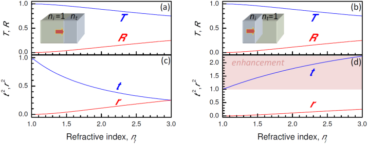
The inset schematically shows the near-side (a,c) and far-side (b,d) excitation cases for SERS. The shaded region in (d) shows the field enhancement (note the different scales on the ordinate axis).
The analysis presented above for plane wave propagation through a boundary from high to low refractive index shows a generic property of the light field enhancement (when the field amplitude is considered rather than far-field intensity).
Discussion
Fresnel enhancement of the E-field can be used to increase the signal intensity in SERS experiments. The observed SERS enhancement in the case of far-side excitation is quantitatively explained, within the limitations of the current experimental results. The explanation is consistent with literature data reported over more than 20 years. While the increased signal levels reported here are relatively small compared to the standard SERS enhancement of 106–108, this additional enhancement is generally applicable and may be combined with other known methods for amplifying the electric field, such as thin film interference effects27, Fabry-Pérot cavities28, whispering gallery modes29 or far-field dipole coupling30. The Fresnel contribution could be further increased by the use of other high refractive index substrates. Further work is required to explore this effect in other substrate materials and to understand how surface roughness and the metal islands themselves affect the Fresnel factor.
There is an interesting analogy between the Fresnel contribution discussed here and the increased surface sensitivity that is found in total internal reflection Raman spectroscopy31. Just as the normal Raman signal can be enhanced at the critical angle in a total internal reflection geometry, so too may the SERS signal be maximized at larger angles of incidence. Since both of these effects appear to be explained by the Fresnel formalism, future work should aim to unify the theory for both SERS and normal Raman.
The angle dependence of the effect must also be investigated in order to account for practical situations where a range of excitation and scattering angles are involved. It was noted earlier that (a) the SERS signal did not increase linearly with solid angle of collection and (b) the extra enhancement for far-side excitation decreased with increasing solid angle. For the metal-island films considered here, these observations can be explained qualitatively by referring to the polarization of the laser light emerging from the microscope objective. The low NA objectives provide the closest approximation to the plane wave situations considered in the FDTD models and in the Fresnel treatment. Higher NA objectives will tend to introduce a perpendicular polarization component with respect to the dielectric surface. This polarization will not be effective in exciting hot spots between neighboring metal particles, thus causing a decrease in the average SERS intensity10. This effect may be further exaggerated due to diffraction in the far-side excitation geometry. Although this is an interesting feature of the current results, it should not divert attention from further investigations of the angular dependence, as there are other SERS substrate geometries with higher dimensionality that provide a more consistent enhancement over a wider range of collection angles32.
Moreover, this additional Fresnel enhancement may be significant in optical fibre SERS and other sensor devices where the collection aperture may be limited in comparison to Raman microscope systems19,20. There are also push-pull forces exerted on the interfaces due to the very same Fresnel scaling laws, since Force = Power/c, where c is velocity of light inside the medium. As light passes through the boundary, a mechanical force is applied33,34. This might affect molecular alignment and stretching of analyte species and be utilized for further control over the SERS signal.
Methods
Substrate fabrication
Glass cover slips of 100 μm thickness were used without any surface pretreatment. The cover slips were mounted on a microscope slide with the aid of vacuum compatible double-sided carbon tape. The samples were then placed inside an Emitech K975X thermal evaporator unit which was operated in two separate stages. In the first stage it was used in a sputtering arrangement for the deposition of a 2-nm chromium (99.99% ProSciTech) adhesion layer on the exposed surface of the cover slip. In the second stage the unit was used as a thermal evaporator to lay down a silver island film by oblique angle deposition (OAD). A nominal coating thickness of 100 nm of silver (99.99%, Sigma-Aldrich) was deposited on the cover slip at an angle of 86° between sample normal and the direction of vapour flux. Coating thickness was measured by a quartz crystal microbalance positioned normal to the vapour flux; the actual film thickness is much smaller. The deposition rate was maintained at 0.05 nm.s−1, while the chamber pressure was maintained at 1 × 10⁻⁴ mbar. This procedure produces a thin metal island film on the surface of the cover slip21,35.
SERS measurements
The cover slips with the OAD nanostructure were functionalized with thiophenol by immersing in a 10 mM ethanolic solution for ten minutes, followed by rinsing in ethanol to remove any unbound molecules. Thiophenol is a convenient SERS reference because it forms a stable self-assembled monolayer on the metal surface36. As a precautionary measure, the uncoated surfaces of the cover slips were cleaned with ethanol and lint free tissue to remove any inadvertently adsorbed metal or thiophenol. The thiophenol SERS spectra were acquired with an InVia Streamline microscope (Renishaw, UK) and 514.5 nm excitation.
The SERS signal was collected through the same objective in a backscattering geometry. The laser power at the sample was ~ 1 mW, but was lower for the high NA objectives. Therefore the data was adjusted for the laser power at the sample for each objective. For comparison purposes, the baseline-to-peak heights of the four strongest thiophenol peaks (1000, 1021, 1072 and 1573 cm−1) were averaged to arrive at a single value for each spectrum.
Author Contributions
S.Ja collected the experimental data, analysed the results and wrote the first draft of the manuscript; L.R. performed the FDTD simulations and contributed to the text; S.Ju identified the Fresnel contribution, calculated the resultant fields and contributed to the text; P.R.S. initiated and coordinated the research and contributed to the text. All authors read and approved the manuscript.
Acknowledgments
This work was supported by the Australian Research Council under Discovery Project grant DP1092955. The authors thank Dr Sharath Sriram (RMIT) for assisting with the SEM analysis.
References
- Stiles P. L., Dieringer J. A., Shah N. C. & Van Duyne R. P. Surface-enhanced Raman spectroscopy. Annu. Rev. Anal. Chem. 1, 601–626 (2008). [DOI] [PubMed] [Google Scholar]
- Kneipp J., Wittig B., Bohr H. & Kneipp K. Surface-enhanced Raman scattering: a new optical probe in molecular biophysics and biomedicine. Theor. Chem. Acc. 125, 319–327 (2010). [Google Scholar]
- Etchegoin P. et al. New limits in ultrasensitive trace detection by surface enhanced Raman scattering (SERS). Chem. Phys. Lett. 375, 84–90 (2003). [Google Scholar]
- Kerker M. Effect of optical constants on calculated values of surface-enhanced Raman scattering. J. Opt. Soc. Am. B-Opt. Phys. 2, 1327–1329 (1985). [Google Scholar]
- Nie S. M. & Emery S. R. Probing single molecules and single nanoparticles by surface-enhanced Raman scattering. Science 275, 1102–1106 (1997). [DOI] [PubMed] [Google Scholar]
- Baker G. A. & Moore D. S. Progress in plasmonic engineering of surface-enhanced Raman-scattering substrates toward ultra-trace analysis. Anal. Bioanal. Chem. 382, 1751–1770 (2005). [DOI] [PubMed] [Google Scholar]
- Moskovits M. Surface-enhanced Raman spectroscopy: a brief retrospective. J. Raman. Spectrosc. 36, 485–496 (2005). [Google Scholar]
- Gersten J. & Nitzan A. Electromagnetic theory of enhanced Raman-scattering by molecules adsorbed on rough surfaces. J. Chem. Phys. 73, 3023–3037 (1980). [Google Scholar]
- Schatz G. C. & Van Duyne R. P. in Handbook of Vibrational Spectroscopy (Eds: Chalmers J. M., & Griffiths P. R.), Wiley, New York, 759–774 (2002). [Google Scholar]
- Jayawardhana S., Rosa L., Buividas R., Stoddart P. R. & Juodkazis S. Light enhancement in surface-enhanced Raman scattering at oblique incidence. Photonic Sensors 2, 283–288 (2012). [Google Scholar]
- Otto A. The ‘chemical' (electronic) contribution to surface-enhanced Raman scattering. J. Raman. Spectrosc. 36, 497–509 (2005). [Google Scholar]
- Lombardi J. R. & Birke R. L. A unified view of surface-enhanced Raman scattering. Acc. Chem. Res. 42, 734–742 (2009). [DOI] [PubMed] [Google Scholar]
- Brown R. J. C. & Milton M. J. T. Nanostructures and nanostructured substrates for surface-enhanced Raman scattering (SERS). J. Raman. Spectrosc. 39, 1313–1326 (2008). [Google Scholar]
- Jennings C., Aroca R., Hor A. M. & Loutfy R. O. Surface-enhanced Raman-scattering from copper and zinc phthalocyanine complexes by silver and indium island films. Anal. Chem. 56, 2033–2035 (1984). [Google Scholar]
- Aroca R., Jennings C., Kovacs G. K., Loutfy R. O. & Vincett P. S. Surface-enhanced Raman scattering of Langmuir-Blodgett monolayers of phthalocyanine by indium and silver island films. J. Phys. Chem. 89, 4051–4054 (1985). [Google Scholar]
- Bello J. M., Stokes D. L. & Vo-Dinh T. Titanium-dioxide based substrate for optical monitors in surface-enhanced Raman-scattering analysis. Anal. Chem. 61, 1779–1783 (1989). [Google Scholar]
- Vo-Dinh T. et al. Surface-active substrates for Raman and luminescence analysis. Talanta 36, 227–234 (1989). [DOI] [PubMed] [Google Scholar]
- Viets C. & Hill W. Single-fibre surface-enhanced Raman sensors with angled tips. J. Raman Spectrosc. 31, 625–631 (2000). [Google Scholar]
- Stoddart P. R. & White D. J. Optical fibre SERS sensors. Anal. Bioanal. Chem. 394, 1761–1774 (2009). [DOI] [PubMed] [Google Scholar]
- Jayawardhana S., Mazzolini A. P. & Stoddart P. R. Collection efficiency of scattered light in single-ended optical fiber sensors. Opt. Lett. 37, 2142–2144 (2012). [DOI] [PubMed] [Google Scholar]
- Jayawardhana S., Kostovski G., Mazzolini A. P. & Stoddart P. R. Optical fiber sensor based on oblique angle deposition. Appl. Opt. 50, 155–162 (2011). [DOI] [PubMed] [Google Scholar]
- Palik E. D. Handbook of Optical Constants of Solids, Academic Press, San Diego (1991). [Google Scholar]
- Kerker M., Wang D. S. & Chew H. Surface enhanced Raman-scattering (SERS) by molecules adsorbed at spherical-particles. Appl. Optics 19, 4159–4174 (1980). [DOI] [PubMed] [Google Scholar]
- McMahon J. M. et al. Gold nanoparticle dimer plasmonics: finite element method calculations of the electromagnetic enhancement to surface-enhanced Raman spectroscopy. Anal. Bioanal. Chem. 394, 1819–1825 (2009). [DOI] [PubMed] [Google Scholar]
- Fang Y., Seong N.-H. & Dlott D. D. Measurement of the distribution of site enhancements in surface-enhanced Raman scattering. Science 321, 388–392 (2008). [DOI] [PubMed] [Google Scholar]
- Hecht E. Optics, 4th ed. Addison-Wesley, San Francisco (2002). [Google Scholar]
- Shoute L. C. T., Bergren A. J., Mahmoud A. M., Harris K. D. & McCreery R. L. Optical interference effects in the design of substrates for surface-enhanced Raman spectroscopy. Appl. Spectrosc. 63, 133–140 (2009). [DOI] [PubMed] [Google Scholar]
- Polemi A. & Shuford K. L. Sensing properties of a Fabry-Perot dielectric structure and dimer nanoparticles. J. Nanotechnol. 2012, 745390 (2012). [Google Scholar]
- White I. M., Gohring J. & Fan X. SERS-based detection in an optofluidic ring resonator platform. Opt. Exp. 15, 17433–17442 (2007). [DOI] [PMC free article] [PubMed] [Google Scholar]
- Pinchuk A. O. & Schatz G. C. Nanoparticle optical properties: Far- and near-field electrodynamic coupling in a chain of silver spherical nanoparticles. Mater. Sci. Eng B 149, 251–258 (2008). [Google Scholar]
- Woods D. A. & Bain C. D. Total internal reflection Raman spectroscopy. Analyst 137, 35–48 (2012). [DOI] [PubMed] [Google Scholar]
- Buividas R., Stoddart P. R. & Juodkazis S. Laser fabricated ripple substrates for surface-enhanced Raman scattering. Ann. der Phys. 524, L5–L10 (2012). [Google Scholar]
- Juodkazis S., Murazawa N., Wakatsuki H. & Misawa H. Laser irradiation induced disintegration of a bubble in a glass melt. Appl. Phys. A 87, 41–45 (2007). [Google Scholar]
- Murazawa N., Juodkazis S., Misawa H. & Wakatsuki H. Laser trapping of deformable objects. Opt. Express 15, 13310–13317 (2007). [DOI] [PubMed] [Google Scholar]
- Driskell J. D. et al. The use of aligned silver nanorod arrays prepared by oblique angle deposition as surface enhanced Raman scattering substrates. J. Phys. Chem. C 112, 895–901 (2008). [Google Scholar]
- Bryant M. A. & Pemberton J. E. Surface Raman-scattering of self-assembled monolayers formed from 1-alkanethiols at Ag. J. Am. Chem. Soc. 113, 3629–3637 (1991). [Google Scholar]


