Abstract
One important use of layered semiconductors such as molybdenum disulfide (MoS2) could be in making novel heterojunction devices leading to functionalities unachievable using conventional semiconductors. Here we demonstrate a metal-semiconductor-metal heterojunction photodetector, made of MoS2 and amorphous silicon (a-Si), with rise and fall times of about 0.3 ms. The transient response does not show persistent (residual) photoconductivity, unlike conventional a-Si devices where it may last 3–5 ms, thus making this heterojunction roughly 10X faster. A photoresponsivity of 210 mA/W is measured at green light, the wavelength used in commercial imaging systems, which is 2−4X larger than that of a-Si and best reported MoS2 devices. The device could find applications in large area electronics, such as biomedical imaging, where a fast response is critical.
Molybdenum disulfide (MoS2), a member of the family of layered transition metal dichalcogenides, has long been used as lubricants1. The interest in electronic and optoelectronic applications of MoS2 thin films has been kindled by recent demonstrations of high mobility transistors with MoS2 active layer2,3. While mono-layer MoS2 is targeted for high end applications such as alternative to silicon transistors2,3,4,5,6,7,8, thin film MoS2 could be suitable for other applications such as displays and thin film sensors9. Recently, thin film MoS2 transistors with mobilities of 70–100 cm2/Vs were demonstrated10,11, which could be used for driving pixels on displays. Phototransistors with thin film MoS2 also showed promise for thin film photodetectors, even though their responsivity at the wavelength of 550 nm was about 50 mA/W10. Among the commercially available thin film photodetectors, amorphous silicon (a-Si) is widely used as the sensing element for several applications including indirect x-ray imagers for radiology12,13,14,15. However, persistent photoconductivity, due to structural defects in amorphous silicon, poses several problems such as slow operation speed (tens of frames per second) and image retention (lag), making it challenging to address high speed applications such as fluoroscopy and tomography12,13,14,15. Therefore, a fast photodetector would significantly advance the state of the art and expand the range of imaging applications where it could be used. We demonstrate that thin film MoS2 and amorphous silicon form a heterojunction diode that results in such a high speed photodetector.
Results
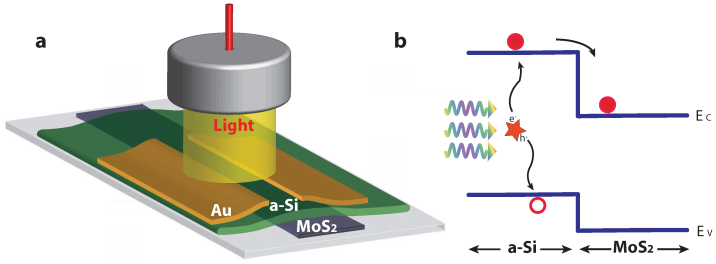
We investigated a lateral metal-semiconductor-metal (MSM) device structure consisting of thin film MoS2 covered with thin film a-Si. This heterostructure made across a Van-der-Waals interface is expected to be robust due to structural stability and chemical inertness of the 2D MoS2 surface and therefore provide a diode-like device without the need for epitaxy. A schematic of the device structure is shown in Fig. 1a. The energy band diagram is shown in Fig. 1b, where an electron affinity of 3.8 and 4.3 and a bandgap of 1.6 and 1.3 eV for a-Si and MoS2, respectively, was assumed11,16,17. In this structure, if photons are absorbed in the a-Si layer, some of photogenerated electrons may diffuse to the a-Si/MoS2 junction and subsequently get swept into the MoS2 side. In general, both layers may contribute to photocurrent. It is important to note, however, that the electrons that get transferred to MoS2 should move with a higher velocity due to a larger mobility of MoS2 as compared to a-Si. Bulk mobility of a-Si is about 10 cm2/Vs18,19, whereas measured mobility of our MoS2 thin films were 2−3X higher (see discussions later). The fast moving electrons in MoS2 are expected to lead to a much faster photoresponse for the a-Si/MoS2 photodetector as compared to the ones based on a-Si only.
Figure 1. Operation concept of molybdenum disulfide amorphous silicon heterojunction photodetector.
(a) schematic and (b) energy band diagram of a-Si/MoS2 heterojunction MSM photodetector. The light is incident from a-Si side, optical absorption occurs in a-Si, and photogenerated electrons diffuse to the underlying MoS2 layer and are transferred across the MoS2 layer toward a metal contact.
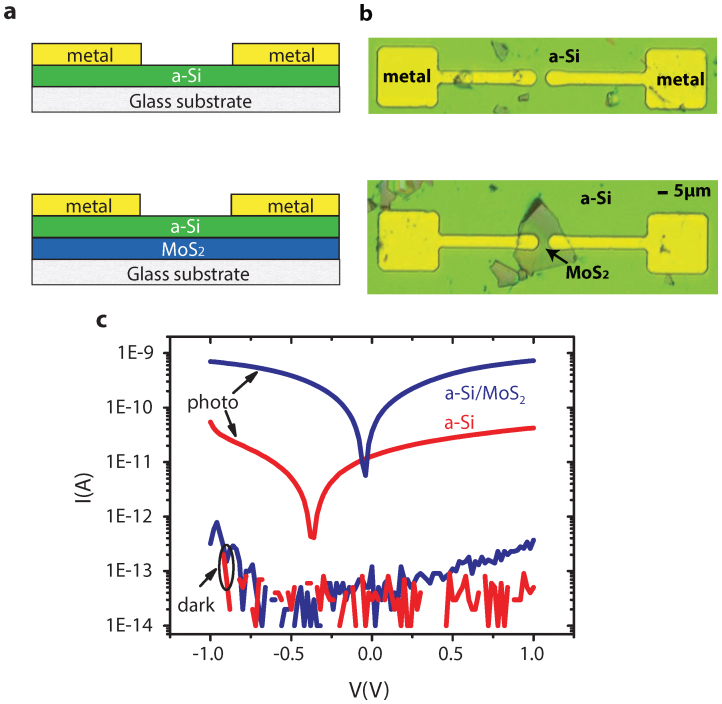
To test this hypothesis, two MSM devices were fabricated on SiO2 substrate. The semiconductor layer consists of a 60 nm mechanically exfoliated MoS2 flake covered by 100 nm a-Si in one device, and the 100 nm a-Si film alone for the second one. The schematic of device cross sections and top view photomicrographs of the fabricated devices are shown in Fig. 2a and b. The length and width of the fabricated devices are roughly 5 and 6 μm, respectively. The current-voltage (IV) characteristics of the devices were measured under dark and illuminated conditions. Figure 2c shows the dark IV characteristics. The dark current of the device with just a-Si active layer is below the noise level of our characterization system which is about 50 fA on average. Low dark currents are expected for a-Si devices as the resistivity of a-Si is above 1010 Ωcm19. The dark current of the hybrid a-Si/MoS2 device is also below the noise level for voltages less than 0.25 V, and increases over the noise level beyond 0.25 V. It is about 0.3 pA at 1 V. Notably, we also evaluated MSM devices with just a thin film MoS2 layer, where we found that the dark current is too high (~40 pA at 1 V) for it to be particularly useful, see Supplementary Materials and Figure S3. The measured photo IV characteristics of the hybrid a-Si/MoS2 and a-Si devices are also shown in Fig. 2c. For this measurement, a fiber-coupled broadband light out of a halogen lamp was used. The optical power density was 10 mW/cm2. As seen, the photocurrent of the hybrid a-Si/MoS2 device is about one order of magnitude larger than that of the a-Si device.
Figure 2.
(a) Schematic of cross sections of two metal-semiconductor-metal (MSM) photodetectors and (b) corresponding top view photomicrograph of devices. The length and width of devices is about 5 and 6 μm, respectively. (c) Measured dark and photo current-voltage (IV) characteristics. The semiconductor layer is 100 nm a-Si film (labeled as a-Si), and 60 nm MoS2 flake covered by 100 nm a-Si (labeled as a-Si/MoS2), see Supplementary Materials and Figure S1 for further details.
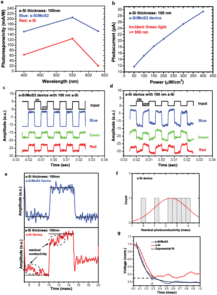
To obtain further insight into the device operation, we measured photoresponse of devices at three wavelengths corresponding to blue, green, and red colors. For these measurements, we used standard LEDs as light sources and the incident power was 0.4 mW/cm2. Photoresponsivity, calculated as the ratio of photocurrent to incident power, is shown in Fig. 3a. As seen, the responsivity of the hybrid a-Si/MoS2 device is larger than that of the a-Si device for all wavelengths. For example, at λ = 400 nm, they are about 150 and 60 mA/W for the hybrid a-Si/MoS2 and the a-Si device, respectively. For λ = 550 nm, the responsivity is maximum which is about 210 mA/W. This responsivity is 4× larger than that of best MoS2 devices10, and 2× larger than that of a-Si devices reported here. The green wavelength is of special interest as x-ray imagers operate at this frequency. At the wavelength of 630 nm, the photoresponse of the hybrid device is seven times larger than that of the a-Si device. The reason for this larger gain is that the a-Si layer does only absorb a part of the incident light at 630 nm and thus the underlying MoS2 is also contributing to photogeneration. This is confirmed by transmittance measurements as a function of wavelength as shown in Fig. 4. We also investigated the photoresponse of the a-Si/MoS2 device, with 100 nm a-Si, when the incident power changes. Fig 3b shows the photocurrent as a function of incident power from 50 to 400 μW/cm2. As seen, it is fairly linear versus the input power.
Figure 3.
(a) Measured photoresponsivity of a-Si/MoS2 and a-Si MSM devices for three wavelengths corresponding to blue, green, and red colors; the thickness of a-Si is 100 nm. Photocurrents at the applied voltage of 1 V were taken for calculations. The incident power was 0.4 mW/cm2. (b) photocurrent of the a-Si/MoS2 device as a function of incident power. Applied voltage was 1 V. (c) and (d) transient responses of the two devices for three incident wavelengths. For part (d), the voltage on the a-Si device was increased to obtain photocurrent pulse amplitudes comparable to that of the hybrid device. (e) The close view of two pulses highlighting the residual conductivity of the a-Si device. (f) statistical distribution of the residual conductivity of the a-Si device. (g) response time extraction and fitting with an exponential function. In parts (a) and (b), lines are for the eye guide only.
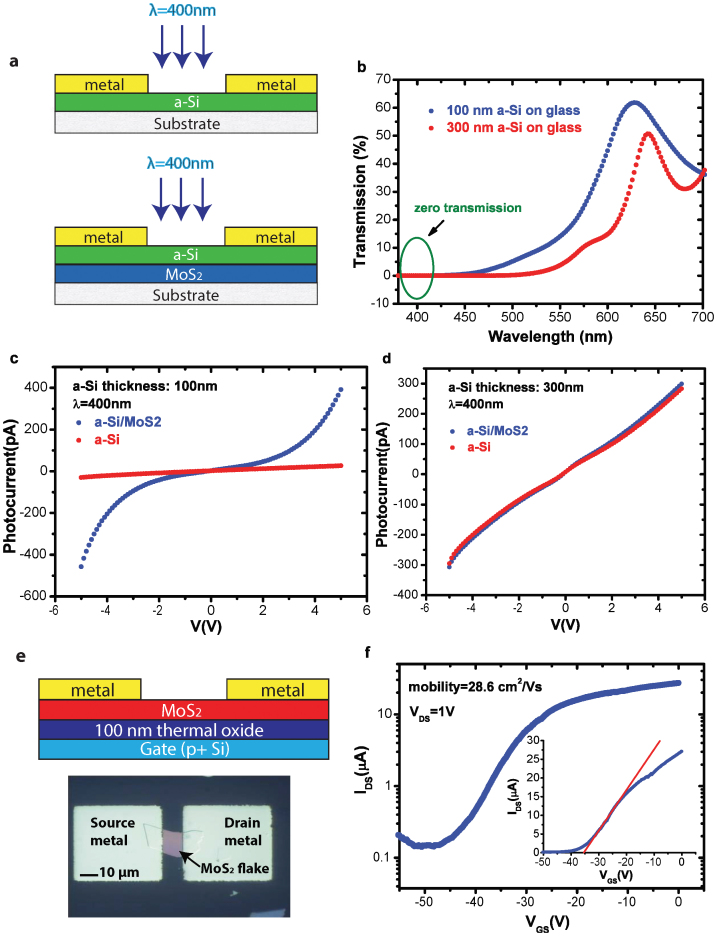
Figure 4. Experimental data that support the proposed concept of operation of the photodetector.
(a) Schematic diagram of devices subjected to blue incident light. (b) Measured UV-visible transmission of 100 and 300 nm a-Si thin films, used in the two sets of devices, with and without MoS2 flakes. (c) Measured photo IV of devices with 100 nm a-Si, showing that the IV of the a-Si/MoS2 device is non-linear and MoS2 is effective in boosting the photocurrent. (d) Measured photo IV of devices with 300 nm a-Si, showing that MoS2 is not effective in enhancing the photocurrent. (e) schematic cross section and top view photomicrograph of the bottom-gate transistor, made of a 73 nm thick MoS2 flake. (f) Measured transfer characteristic where a mobility of 28.6 cm2/Vs was extracted.
Next we measured the transient response of both set of devices by pulsing the incident light by biasing the LEDs with a 3 V, 100 Hz square voltage out of a function generator. The results are shown in Figs. 3c and 3d. As seen, the response of the a-Si/MoS2 device does not show residual conductivity, i.e. the pulses are well defined and on/off levels are more stable and cleaner. However, there is persistent (residual) conductivity in the response of the a-Si sample. Figure 3e shows a close view of two pulses. It is evident that the residual conductivity of the a-Si device may last for about 3 msec. Indeed, the existence of residual conductivity in a-Si photodetectors of the order of a few msec is very well-known12,13,14,15. For example, in Ref. [14], a value of 5 msec was reported. To determine the time of residual conductivity in our devices, we plotted the statistical distribution of the residual conductivity of the a-Si device, shown in Figure 3f, which clearly shows a 3–5 msec average. Note that, for some pulses, the conductivity never reaches the steady state before the next pulse arrives. We have ignored those pulses. Thus this estimated average time should be considered to be a lower bound. For practical imaging applications the residual conductivity of a-Si limits the operation speed, because one has to wait 3–5 msec for it to vanish.
Now, let us look at the rise and fall times. We defined the fall and rise times as the time it takes to switch from one level to about 90% of the second level. Figure 3g shows one example, where the response pulses are normalized. As seen, a response time of 0.3 ms is extracted for both devices. Using the data from Figs 3c and 3d, we also obtained statistical information of the transient response. The data are summarized in Supplementary Figures S5–6. In addition, the transient response of the hybrid device can be modeled with an exponential function, y = y0 + A exp (−t/t0), where t0 is the time constant. The t0 is about 170 μsec and its statistical distribution is shown in Supplementary Fig. S7. These observations can now be summarized in the following way: both photodetectors show similar rise and fall times which are of the order of 0.3 msec. However for a-Si devices, there exists a residual photoconductivity, as it is well-known in literature12,13,14,15, that limits its speed to 3–5 msec. For the heterojunction device, on the other hand, the residual conductivity is not present, making it possible to use it right after the initial fall time. Comparing these two timings, we conclude that the imaging speed can be increased by 10X.
Thus far, based on the photoresponsivity data, one may conclude that the junction between the MoS2 and a-Si enhances the performance by ensuring that a part of photogenerated electrons inside the a-Si that survive and diffuse to the junction are swept to the MoS2 side. To test what happens for a thicker a-Si, we made another set of devices with 300 nm a-Si with the same dimensions as those of the first set (Note that the diffusion length of a-Si is about 300 nm19). Supplementary Fig. S4 shows the photoresponsivity data measured under similar conditions like before. As seen, devices with 300 nm a-Si, with and without MoS2, give the same photoresponse for all three incident lights. Therefore, in this case, photogenerated electrons completely reside inside the a-Si layer. Compared to the devices with 100 nm a-Si, the ones with 300 nm a-Si give larger photocurrents and, for example, at λ = 550 nm the responsivity is about 1 A/W. As for the dynamic response, both devices show similar speed of about 3 msec, see Supplementary Figures S8 and S9. This observation indicates that the MoS2 junction is beneficial and results in a fast photoresponse when the thickness of a-Si is less than the diffusion length of electrons, so that electrons survive to reach the junction and be transferred to the MoS2. Similar transient responses were measured for all three wavelengths; see Supplementary Figures S8–9. Notably, when a-Si thickness is 300 nm, the photocurrent is higher compared to when it is 100 nm because the volume of absorption is now much larger. Therefore, we conclude that there exists a trade-off between speed and amplitude of photocurrent in this heterojunction. While the larger mobility of MoS2 helps increase the speed of the device, a smaller thickness of a-Si, which is needed to ensure that electrons can reach the junction before recombining, could lead to reduced absorption and therefore smaller photocurrent. By varying the thickness of a-Si and MoS2 layers, it should be possible to obtain an optimized scenario where a substantial increase in speed can be gained without giving up the photocurrent significantly.
Before concluding, we provide additional experimental measurements that elucidate the physics of charge transfer from a-Si into the underlying MoS2 at the junction. Fig. 4a shows two sets of devices with 100 and 300 nm a-Si, with and without MoS2, that were subjected to an incident light of λ = 400 nm. The reason to choose this wavelength is that it is completely absorbed in the top a-Si layer without reaching the MoS2. Fig. 4b shows transmission measurements of a-Si in the UV-visible range where below 420 nm the transmission is virtually zero. This implies that in the a-Si/MoS2 devices the MoS2 is not receiving any blue light. However, MoS2 is electrically active as deduced from the IV data shown in Fig. 4c, for the devices with 100 nm a-Si. As seen, the IV of the a-Si device is linear, but that of the hybrid a-Si/MoS2 device is non-linear and larger. This validates the assumption made in the beginning that MoS2 and a-Si form a diode where part of photogenerated electrons diffuse from a-Si towards the junction and are swept into the MoS2. When the a-Si is 300 nm thick, both IVs are the same and fairly linear, see Fig. 4d. This implies that there is no charge transfer from 300 nm a-Si into the MoS2 layer. In addition, we mentioned that transferred electrons move with a higher mobility in MoS2 and this contributes to the larger photocurrent of the hybrid device. To support this argument, we made a bottom-gate transistor out of thin film MoS2 on thermally grown SiO2 as the gate dielectric. The schematic of cross section and the top view photomicrograph of the transistor are shown in Fig. 4e. The transfer characteristic is shown in Fig. 4f. A mobility of 28.6 cm2/Vs was extracted from the linear plot of the curve, as shown in the inset of Fig. 4f. This value is larger than that of the bulk of a-Si, about 10 cm2/Vs18,19. Thus the higher mobility of MoS2 is effective in enhancing the photoresponse of the hybrid photodetector.
Discussion
The a-Si/MoS2 photodetector could be used for biomedical imaging applications where a fast photoresponse is required. For example, currently, flat-panel x-ray imagers based on a-Si p-i-n photodetectors operate at frame rates in the range of 10–100 Hz, limited by the slow photoresponse of a-Si. The detector presented here may offer a speed of operation up to several kHz, considering its rise and fall times of 0.3 ms. The fast response also allows shorter x-ray exposure times to patients which helps to reduce the health hazards of x-ray radiation. From technology point of view, the advantage of this detector is its simplicity of fabrication which can be easily integrated with other components and readout circuits. From device and structure point of view, the layered material MoS2 and, in general, the family of metal dichalcogenides, do not form strong chemical bonds with other materials. The bonding is mainly due to Van-der-Waals forces. Thus they may enable a new class of devices, Van-der-Waals heterojunctions, by forming a wide range of 2D/2D and 2D/3D heterostructures20. Finally, for practical applications, large area growth methods such as CVD should be developed. Research in this direction is underway by several groups.
In conclusion, we demonstrated that molybdenum disulfide forms a heterojunction diode with amorphous silicon which leads to a 10X faster response compared to the state of the art. The device has a photoresponsivity of about 210 mA/W at the wavelength of 550 nm. In addition, it has a low dark current of 0.3 pA at 1 V bias. Going forward, such devices could be integrated with MoS2 transistors, as readout circuits and pixel amplifiers, leading to a monolithic large area technology based on layered semiconductors.
Methods
Flakes of MoS2 were exfoliated on SiO2 substrates from a piece of MoS2 crystal (provided by the SPI Supplies, www.2spi.com) using the scotch-tape mechanical cleavage method. Subsequently, the thin film MoS2 flakes were coated with amorphous silicon (a-Si) thin films, deposited by plasma-enhanced chemical vapour deposition (PECVD) using silane gas source at 260 C. Metal contacts were formed by the conventional lift-off technique, where Ti (20 nm) and Au (160 nm) were deposited by electron-beam evaporation at room temperature. Current-voltage characteristics of devices were measured by an Agilent 4155C semiconductor parameter analyzer, under dark and illuminated conditions. For the latter, a fiber-coupled broadband light out of a halogen lamp was used. The optical power density was about 10 mW/cm2. We also measured photoresponse of devices at three wavelengths corresponding to blue, green, and red colors. For these measurements, we used standard LEDs as light sources and the incident power was about 0.4 mW/cm2. All measurements were done at room temperature.
Author Contributions
M.E. and S.S. devised the device concept and initiated the research. M.E. worked on device fabrication, performed measurements, and wrote the manuscript. All the authors read and commented on the manuscript.
Supplementary Material
Supplementary Materials
Acknowledgments
This research was supported in part by NSF CAREER grant #1149809 and a DARPA/ARO grant #W911NF-12-1-0351. M.E. acknowledges Natural Sciences and Engineering Research Council of Canada postdoctoral fellowship. The authors are grateful to Asis Sarkar, Asif Khan, Long You, Chun Wing Yeung, and Umar Shafique for assisting with samples preparation and characterization. The authors would also like to thank Richard Barber and William Wong, of the University of Waterloo, for facilitating access to the G2N laboratory.
References
- Bichsel R. & Levy F. Influence of process conditions on the electrical and optical properties of RF magnetron sputtered MoS2 films. J. Phys. D: Appl. Phys. 19, 1809–1819 (1986). [Google Scholar]
- Radisavljevic B., Radenovic A., Brivio J., Giacometti V. & Kis A. Single-layer MoS2 transistors. Nat. Nanotechnol. 6, 147–150 (2011). [DOI] [PubMed] [Google Scholar]
- Lee H. S. et al. MoS2 Nanosheet Phototransistors with Thickness-Modulated Optical Energy Gap. Nano Lett. 12, 3695–3700 (2012). [DOI] [PubMed] [Google Scholar]
- Yang H. et al. Graphene Barristor, a Triode Device with a Gate-Controlled Schottky Barrier. Science 336, 1140–1143 (2012). [DOI] [PubMed] [Google Scholar]
- Qiu H. et al. Electrical characterization of back-gated bi-layer MoS2 field-effect transistors and the effect of ambient on their performances. App. Phys. Lett. 100, 123104-1-3 (2012). [Google Scholar]
- Wang H. et al. Integrated Circuits Based on Bilayer MoS2 Transistors. Nano Lett. 12 (9), 4674–4680 (2012). [DOI] [PubMed] [Google Scholar]
- Liu H. & Ye P. D. MoS2 Dual-Gate MOSFET With Atomic-Layer-Deposited Al2O3 as Top-Gate Dielectric. IEEE Elec. Dev. Lett. 33, 546–548 (2012). [Google Scholar]
- Yin Z. et al. Single-Layer MoS2 Phototransistors. ACS Nano 6(1), 74–80 (2012). [DOI] [PubMed] [Google Scholar]
- Kim E. S. et al. Multilayer Transition-Metal Dichalcogenide Channel Thin-Film Transistors. Tech. Digest IEEE IEDM, IEDM12-108-111 (2012). [Google Scholar]
- Choi W. et al. High-Detectivity Multilayer MoS2 Phototransistors with Spectral Response from Ultraviolet to Infrared. Advanced Materials 24, 5832–5836 (2012). [DOI] [PubMed] [Google Scholar]
- Kim S. et al. High-mobility and low-power thin-film transistors based on multilayer MoS2 crystals. Nature Communications 3, Article number:1011 (2012). [DOI] [PubMed] [Google Scholar]
- Granfors P. R. & Albagli D. Scintillator-based flat-panel x-ray imaging detectors. J. Society for Information Display 17/6, 535–542 (2009). [Google Scholar]
- Siewerdsen J. H. & Jaffray D. A. A ghost story: Spatio-temporal response characteristics of an indirect-detection flat-panel imager. Med. Phys. 26(8), 1624–1641 (1999). [DOI] [PubMed] [Google Scholar]
- Takayama S., Mori K., Suzuki K. & Tanuma C. An a-Si:H Photoconductive Sensor with a Gate Electrode. IEEE Trans. Electron Devices 40, 342–347 (1993). [Google Scholar]
- Seibert J. A. Flat-panel detectors: how much better are they? Pediatr Radiol 36 (Suppl 2), 173–181 (2006). [DOI] [PMC free article] [PubMed] [Google Scholar]
- Park N.-M., Kim T.-S. & Park S.-J. Band gap engineering of amorphous silicon quantum dots for light-emitting diodes. Appl. Phys. Lett. 78, No. 17, 2575–2577 (2001). [Google Scholar]
- Kabir M. I. et al. Bandgap Optimization of Absorber Layers in Amorphous Silicon Single and Multijunction Junction Solar Cells. Chalcogenide Letters 9, No. 1, 51–59 (2012). [Google Scholar]
- Shur M. S., Slade H. C., Jacunski M. D., Owusu A. A. & Ytterdal T. SPICE Models for Amorphous Silicon and Polysilicon Thin Film Transistors. J. Electrochem. Soc. 144, 2833–2839 (1997). [Google Scholar]
- Poortmans J. & Arkhipov V. Thin Film Solar Cells Fabrication, Characterization and Applications. (John Wiley and Sons Ltd, West Sussex, 2006), pp. 181–184.
- Kang J., Tongay S., Zhou J., Li J. & Wu J. Band offsets and heterostructures of two-dimensional semiconductors. App. Phys. Lett. 102, 012111-1-3 (2013). [Google Scholar]
Associated Data
This section collects any data citations, data availability statements, or supplementary materials included in this article.
Supplementary Materials
Supplementary Materials


