Abstract
Point-functionalized carbon nanotube field-effect transistors can serve as highly sensitive detectors for biomolecules. With a probe molecule covalently bound to a defect in the nanotube sidewall, two-level random telegraph noise (RTN) in the conductance of the device is observed as a result of a charged target biomolecule binding and unbinding at the defect site. Charge in proximity to the defect modulates the potential (and transmission) of the conductance-limiting barrier created by the defect. In this Letter, we study how these single-molecule electronic sensors are affected by ionic screening. Both charge in proximity to the defect site and buffer concentration are found to affect RTN amplitude in a manner that follows from simple Debye length considerations. RTN amplitude is also dependent on the potential of the electrolyte gate as applied to the reference electrode; at high enough repulsive potentials, the target DNA is completely repelled and RTN is suppressed.
Keywords: Debye screening, carbon nanotube, single-molecule detection, Coulomb potential, DNA, microfluidics
Nanoscale field-effect transistors such as nanowires and carbon nanotubes have been used as ultra-sensitive gas, chemical and biological sensors.1–6 Carbon nanotubes are particularly promising because they are one-dimensional conductors with an exposed channel and a very large surface-to-volume ratio. Previous experiments involving label-free detection of proteins and DNA have determined that conductance modulation of the nanotube is due to both the electrostatic gating of the channel and the modulation of the Schottky barriers near the contacts.3,5,7,8 These initial efforts, however, did not demonstrate enough sensitivity to detect single molecules and are characterized by high device-to-device variability.
Point functionalization of the nanotube channel, which creates a conductance-dominating scatterer as well as a chemically reactive site for molecular attachment, greatly enhances the sensitivity of the device to charge in the region of the defect. 9,10 In our own recent work, we have shown the appearance of two-level random telegraph noise (RTN) in the conductance of the device as a result of a biomolecule binding and unbinding from the defect site thereby modulating the transmission through the defect.11 This RTN data can be analyzed to study the kinetics and thermodynamics of the interaction by monitoring the conductance as a function of temperature. In this case, all the information extracted from the sensor is contained in the dynamics of the conductance transitions. In this Letter, we instead examine the conductance magnitude of the two-level RTN as a function of the distance between the biomolecule and the nanotube and as a function of buffer concentration.
Previous sensing experiments with nanowire field-effect transistors have demonstrated that charges on biomolecules can be screened by increasing the distance of the biomolecule from the nanowire surface12 or by increasing the buffer concentration.13,14 We demonstrate that the single-molecule response of these devices is also screened by the counterions in the buffer solution. As a result, Debye screening constitutes an important design consideration for label-free single-molecule detection in order to maximize RTN signal by optimizing buffer concentrations, linker and molecular arrangements, and applied electric fields.15
The fabrication method for the point functionalized carbon nanotube devices was described previously.11 Briefly, chemical vapor deposition is used to grow carbon nanotubes on a silicon substrate with a 300-nm thermal oxide. Titanium electrodes are patterned by standard photolithography for source and drain contacts. Another lithography step is used to cover a selected nanotube and remove all others by an oxygen plasma etch. Finally, an on-chip platinum electrode is evaporated for use as a pseudo reference electrode. The chip is annealed at 340 °C for 3.5 h in a forming gas to remove the resist residue and then wire-bonded and assembled in a microfluidic setup with a polydimethylsiloxane (PDMS) mold as shown in Fig. 1a (See supporting information for more details on the microfluidic setup). The point defect in the carbon nanotube sidewall is introduced by a conductance controlled electrochemical oxidation in 1 M sulfuric acid followed by a 45 s immersion in 6.5 mM potassium permanganate16. A probe DNA with an amine group at the 5' end is then covalently attached to the carboxylic acid defect through a standard coupling reaction using sulfo-N-hydroxysuccinimide (sulfo-NHS) and 1-ethyl-3-(3-dimethylaminopropyl)carbodiimide (EDC).
Figure 1. Microfluidic delivery system.
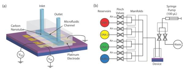
a, Chip with nanotube devices is wire bonded and encapsulated in a PDMS microfluidic cell. b, Digitally controlled pinch valves and manifolds can automatically deliver solutions into and out of the microfluidic channel with a syringe pump.
The Debye length studies described in this report are facilitated by a microfluidic system shown in Fig. 1b. Different aqueous solutions (with different target DNA or ionic concentrations) can be automatically drawn into the channel with the nanotube devices. Digitally controlled pinch valves, manifolds (NResearch Incorporated), and a syringe pump are used to selectively pull and push solutions from reservoirs into a microfluidic channel and into a waste reservoir. In order to avoid solution mixing, solutions are split up into 120 μL intervals that are separated by ~20 μL air gaps. To deliver a new solution into the channel, a Labview program (National Instruments) automatically cycles through a combination of pulling solution into the fluid lines, pulling an air gap, and finally pushing out solution into the waste reservoir. In this way, the fluid channel above the devices can be first flushed by buffer solution and then the selected solution can be introduced automatically. We have verified that the variation in the solution volume is less than ~20 μL when pulling solution into the channel. This setup provides the controlled fluidic platform for the experiments outlined in this Letter.
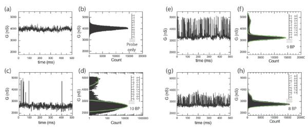
After overnight coupling of the probe oligonucleotide NH2-5'-GTGAGTTGTT-3' to the carbon nanotube defect, we characterize conductance of the carbon nanotube in 1X PBS buffer. In previous studies, we have examined the conductance at different temperatures with and without adding complementary DNA target.11 Now the temperature is set to 17°C with a circular heater/refrigerator and different solutions are introduced into the channel. After turning off the fluid flow and equilibrating the temperature, the conductance is measured for periods of eight minutes at a constant pseudo reference potential of −0.3V, applied to the on chip platinum electrode (see Supporting Information). Without complementary target DNA, the device shows a conductance that is dominated by flicker noise as shown in Fig. 2a and only contains a single state (Fig 2b). Different lengths of target complementary oligonucleotides are now added at 1 μM concentration and the device is again measured for each nucleotide without flow after the equilibrium temperature is reached.
Figure 2. Real time measurements of binding kinetics with different target DNA.
Real-time conductance recording at Vsd=100mV and VPt=−0.3V showing a small interval from an 8 minute recording. a Conductance recording in 1X PBS buffer solution without target DNA. c,e,g Conductance recording with 10, 9 and 8 base pair complementary target DNA. b,d,f,h Conductance based histograms from 30 s time intervals (of which Fig. 2a,b,e,f are small subsets).
Fig. 2c shows the real-time conductance with the corresponding histogram in Fig. 2d for an exactly complementary ten-base-pair target DNA (5'-AACAACTCAC-3'). The conductance fluctuation is similar to previous measurements11, and the device is mostly in the low (bound) state with occasional large but very short spikes corresponding to brief intervals in which the probe DNA is unbound to complementary target. This behavior is expected because at 17°C, the temperature is well below the melting point and the DNA is mostly in the duplex state11. Overall, we have fabricated seven devices with a low temperature normalized RTN amplitude of 66.2±20.6% and similar temperature dependent fluctuations (see Supporting Information).
Fig. 2e shows the two-level RTN observed for a complementary nine-base-pair oligonucleotide, one base pair shorter at the 3' end of the target (5'-AACAACTCA-3'), where the 3'end is closest to the carbon nanotube. The amplitude of the two-level RTN is lower in this case as is also evident in the histogram of Fig. 2f. We also observe an increase in the time spent in the high (unbound) state, which indicates that the melting curve has shifted toward lower temperature, as expected for a shorter DNA target. For the complementary eight-base-pair oligonucleotide (5'-AACAACTC-3'), shortened now by two based at the 3' end, the amplitude of the RTN further decreases as shown in Fig. 2g and in the histogram in Fig. 2h. Even though we have observed a small overall decrease in the conductance over several cycles, which we attribute to non-specific adsorption of target DNA to the sidewall, the fluctuations are repeatable over multiple cycles of flushing buffer and complementary target DNA. In Fig. 3a, we plot the normalized change in resistance, ΔR/R as a function of different target lengths. The RTN amplitude decreases with reduction of the target sequence length at the 3' end.
Figure 3. Effect of removing nucleotides close to the nanotube.
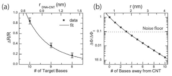
a, Normalized resistance change as a function of length of the target DNA. Nucleotides of the target DNA are removed from the 3' end, closest to the carbon nanotube. Error bars are calculated from at least 5 different 30s time interval histograms. b, Plot of Eqn. 2 as a function of distance for a Debye length of λD=0.70 nm (1X PBS). Base pairs further out are almost completely screened by the counterions. The noise floor is calculated for a signal-to-noise ratio of one using the full width at half maximum (FWHM) of the gaussian fits in the histograms in Fig. 2d,g and h for the noise amplitude.
To explain the length effect on RTN amplitude, we use Debye screening theory. When a charged molecule is placed in a buffer solution, electrostatic interactions cause counterions to surround the molecule, partially offsetting the molecular charge. A very simple approximation of the resulting screened electric potential from a point charge Q is given by the Debye-Hückel model17 as
| (1) |
where ε0 is the dielectric constant, d is the distance from the charge, and λD is the Debye length, given by18
| (2) |
Here, lB is the Bjerrum length, ρi and zi are the ion density and valence for ion species i. That is, the potential decreases exponentially with distance and the Debye length sets the length scale at which the potential approaches zero.
In Fig 3b, we plot the change in potential (ΔΦ) normalized to change in potential for the 10-mer target (ΔΦ0) as determined by Eqn. 1 as a function of the distance between the defect and the position of the first nucleotide on 3' end of the target. Assuming that the DNA is upright and each base is separated by 0.33 nm19 (the three-carbon linker was estimated to be around 0.697 nm long), bases more than 2 nm away from the nanotube lead to changes in the potential smaller than the noise level (flicker noise) in 1X PBS buffer solution. The data in Fig 3a can be represented as a function of distance between the defect and the first target nucleotide and fit with Eqn. 1. To simplify this analysis, we assume that all of the DNA targets have fixed charge despite having varying lengths. This is justified because at most only the three bases on the 3' end contribute to the potential at the defect. We further assume that the resistance change in the nanotube is proportional to the change in potential at the defect. This is valid since the simulated potential is typically between 8 and 15 mV (see Supporting Information), considerably smaller than the thermal voltage. Excellent agreement is found with the measured data with an extracted value of the Debye length of 0.73 nm, slightly larger than the 0.70 nm predicted from Eqn. 2. Of course, the real interaction between the nanotube and the DNA is three-dimensional including the double-helix structure of the DNA. The crystal structure (see Supporting Information) predicts a distance of 1.8–2.2 nm depending on the orientation of the DNA.
Fig. 4 shows how the RTN amplitude for the 8-mer hybridization target depends on the buffer concentration, which modulates the Debye length of the counterions in solution. Here we use five different buffer concentrations of PBS buffer: 10X, 5X, 1X, 0.4X and 0.1X. Reducing the buffer concentration increases the Debye length, which leads to an increase in the RTN amplitude. At the highest buffer concentration (10X PBS), the target DNA charge is completely screened such that the RTN is below the noise floor. We have fit the data in Fig. 4 to Eqn. 1 and extracted an average distance between the target DNA charge and the defect of approximately 1.79 nm. Again, if we assume that each DNA is upright and that each base is separated by 0.33nm with a linker length of 0.697 nm, this yields an expected distance of 1.36 nm. Taking into account the double helix structure of the DNA molecule, the crystal structure (see Supporting Information) predicts a distance of around 1.8–2.2 nm depending on the orientation of the DNA.
Figure 4. Effect of Debye length.
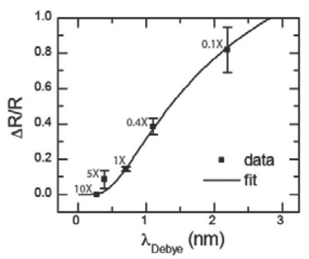
Normalized resistance change as a function of buffer concentration. Increasing the buffer concentration will reduce the Debye length so that more of the DNA's negative charge will be screened by counterions. Error bars are calculated from at least 5 different 30s time interval histograms.
In our previous analyses, we have assumed that the hybridized double-stranded DNA molecule is standing “upright” from the surface. In principle it may actually be at an angle to the surface. In particular, we expect that there is a strong electrostatic interaction between the DNA molecule and the surface of the carbon nanotube such that the potential difference between the liquid and the nanotube will affect the angle of the DNA, similar to previous experiments with DNA on metal electrodes.20,21 In Fig. 5, we investigate the effect of the potential difference (VPt) between the solution and the carbon nanotube on the RTN amplitude using the 10-mer DNA target (5'-AACAACTCAC-3') in 1X PBS. As shown in the gate sweep in inset of Fig. 5a, the pristine device has a charge neutrality point of around −0.2V compared to the platinum reference electrode. Biasing the carbon nanotube device at a potential higher (lower) than the neutrality point will induce electrons (holes) in the nanotube and cause a repulsive (attractive) electrostatic force with the negatively charged DNA. The inset of Fig. 5a also shows the conductance variation with VPt for the defected device with probe DNA attached. We note that the observed RTN amplitudes are larger than what would be predicted from (dG/dVPt)ΓΦ for the probe-attached nanotube by approximately a factor of 50, indicating that the localization of the field-effect of the target DNA charge probably results in considerably more modulation of the barrier due to the point-functionalized defect than global gating.
Figure 5. Effect of applied electric field.
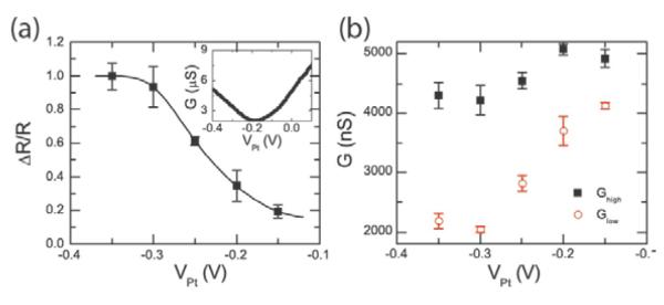
a, RTN amplitude as a normalized resistance change given as a function of electrode potential. The data points are connected by interpolation. Inset shows conductance as a function of solution potential for the pristine device and the functionalize device with probe DNA attached in 1X PBS. The charge neutrality point for the pristine device is around −0.2 V. Error bars are calculated from at least five different 30s time interval histograms. b, High and low conductance at different applied on-chip platinum electrode potentials.
In Fig. 5a, we monitor both states of the RTN signal at different potentials as set by the on-chip platinum electrode. The low-conductance state (with the DNA in the duplex state) is much more dependent on the potential compared to the high-conductance state (with probe DNA only). This is consistent with previous studies, which demonstrate that the orientation of surface-immobilized double-stranded DNA is more strongly affected by electric fields because of its long persistence length (50 nm) compared to single stranded DNA (2nm).20 Fig. 5a shows that the normalized RTN amplitude (as primarily determined by the change in the low-conductance state) increases with more negative solution potentials, consistent with DNA that is leaning towards the carbon nanotube and thereby increasing the potential at the nanotube surface (electrostatic simulations are presented in the Supporting Information). The RTN transitions vanish at high potentials (VPt>−0.1V) indicating that DNA hybridization is inhibited by the negative surface potential.
We have presented experimental results demonstrating the importance of Debye screening for single-molecule field-effect sensors based on carbon nanotubes. The amplitude of RTN fluctuations characterizing single-molecule interactions increases by moving charges closer to the defect or by decreasing the buffer concentration, as supported by simple screening arguments. The results presented here are not only significant to basic scientific research but also important to understand potential applications of these devices as a single-molecule label free sensing platform.
Supplementary Material
Reference
- 1.Kong J, et al. Nanotube molecular wires as chemical sensors. Science. 2000;287:622–625. doi: 10.1126/science.287.5453.622. [DOI] [PubMed] [Google Scholar]
- 2.Staii C, Johnson AT. DNA-decorated carbon nanotubes for chemical sensing. Nano Letters. 2005;5:1774–1778. doi: 10.1021/nl051261f. [DOI] [PubMed] [Google Scholar]
- 3.Heller I, et al. Identifying the mechanism of biosensing with carbon nanotube transistors. Nano Letters. 2008;8:591–595. doi: 10.1021/nl072996i. [DOI] [PubMed] [Google Scholar]
- 4.Chen RJ, et al. Noncovalent functionalization of carbon nanotubes for highly specific electronic biosensors. Proc Natl Acad Sci U S A. 2003;100:4984–4989. doi: 10.1073/pnas.0837064100. [DOI] [PMC free article] [PubMed] [Google Scholar]
- 5.Besteman K, Lee J-O, Wiertz FGM, Heering HA, Dekker C. Enzyme-Coated Carbon Nanotubes as Single-Molecule Biosensors. Nano Letters. 2003;3:727–730. [Google Scholar]
- 6.Zheng G, Patolsky F, Cui Y, Wang WU, Lieber CM. Multiplexed electrical detection of cancer markers with nanowire sensor arrays. Nature Biotechnol. 2005;23:1294–1301. doi: 10.1038/nbt1138. [DOI] [PubMed] [Google Scholar]
- 7.Star A, et al. Label-free detection of DNA hybridization using carbon nanotube network field-effect transistors. Proc. Natl. Acad. Sci. U. S. A. 2006;103:921–926. doi: 10.1073/pnas.0504146103. [DOI] [PMC free article] [PubMed] [Google Scholar]
- 8.Chen RJ, et al. An investigation of the mechanisms of electronic sensing of protein adsorption on carbon nanotube devices. J. Am. Chem. Soc. 2004;126:1563–1568. doi: 10.1021/ja038702m. [DOI] [PubMed] [Google Scholar]
- 9.Khalap VR, Sheps T, Kane AA, Collins PG. Hydrogen Sensing and Sensitivity of Palladium-Decorated Single-Walled Carbon Nanotubes with Defects. Nano Letters. 2010;10:896–901. doi: 10.1021/nl9036092. [DOI] [PubMed] [Google Scholar]
- 10.Goldsmith BR, Coroneus JG, Kane AA, Weiss GA, Collins PG. Monitoring Single-Molecule Reactivity on a Carbon Nanotube. Nano Letters. 2008;8:189–194. doi: 10.1021/nl0724079. [DOI] [PubMed] [Google Scholar]
- 11.Sorgenfrei S, et al. Label-free single-molecule detection of DNA-hybridization kinetics with a carbon nanotube field-effect transistor. Nature Nanotechnology. 2011;6:125–131. doi: 10.1038/nnano.2010.275. [DOI] [PMC free article] [PubMed] [Google Scholar]
- 12.Zhang G-J, et al. DNA Sensing by Silicon Nanowire: Charge Layer Distance Dependence. Nano Letters. 2008;8:1066–1070. doi: 10.1021/nl072991l. [DOI] [PubMed] [Google Scholar]
- 13.Gao XPA, Zheng GF, Lieber CM. Subthreshold Regime has the Optimal Sensitivity for Nanowire FET Biosensors. Nano Letters. 2010;10:547–552. doi: 10.1021/nl9034219. [DOI] [PMC free article] [PubMed] [Google Scholar]
- 14.Stern E, et al. Importance of the Debye Screening Length on Nanowire Field Effect Transistor Sensors. Nano Letters. 2007;7:3405–3409. doi: 10.1021/nl071792z. [DOI] [PMC free article] [PubMed] [Google Scholar]
- 15.Prisbrey L, Schneider G, Minot E. Modeling the Electrostatic Signature of Single Enzyme Activity. The Journal of Physical Chemistry B. 2010;114:3330–3333. doi: 10.1021/jp910946v. [DOI] [PubMed] [Google Scholar]
- 16.Goldsmith BR, et al. Conductance-Controlled Point Functionalization of Single-Walled Carbon Nanotubes. Science. 2007;315:77–81. doi: 10.1126/science.1135303. [DOI] [PubMed] [Google Scholar]
- 17.Debye P, Huckel E. The theory of electrolytes I. The lowering of the freezing point and related occurrences. Physikalische Zeitschrift. 1923;24:185–206. [Google Scholar]
- 18.Israelachvili JN. Intermolecular and surface forces. Academic Press; London; San Diego: 1991. [Google Scholar]
- 19.Mandelkern M, Elias JG, Eden D, Crothers DM. The Dimensions of DNA in Solution. J. Mol. Biol. 1981;152:153–161. doi: 10.1016/0022-2836(81)90099-1. [DOI] [PubMed] [Google Scholar]
- 20.Rant U, et al. Switchable DNA interfaces for the highly sensitive detection of label-free DNA targets. Proc. Natl. Acad. Sci. U. S. A. 2007;104:17364–17369. doi: 10.1073/pnas.0703974104. [DOI] [PMC free article] [PubMed] [Google Scholar]
- 21.Kelley SO, et al. Orienting DNA Helices on Gold Using Applied Electric Fields. Langmuir. 1998;14:6781–6784. [Google Scholar]
Associated Data
This section collects any data citations, data availability statements, or supplementary materials included in this article.


