Abstract
Resistive memory has attracted a great deal of attention as an alternative to contemporary flash memory. Here we demonstrate an interesting phenomenon that multimode resistive switching, i.e. threshold-like, self-rectifying and ordinary bipolar switching, can be observed in one self-assembled single-crystalline ZnO nanoisland with base diameter and height ranging around 30 and 40 nm on Si at different levels of current compliance. Current-voltage characteristics, conductive atomic force microscopy (C-AFM), and piezoresponse force microscopy results show that the threshold-like and self-rectifying types of switching are controlled by the movement of oxygen vacancies in ZnO nanoisland between the C-AFM tip and Si substrate while ordinary bipolar switching is controlled by formation and rupture of conducting nano-filaments. Threshold-like switching leads to a very small switching power density of 1 × 10³ W/cm2.
Traditional charge-based memory technologies are currently facing theoretical and physical limits of downscaling because they become increasingly difficult to reliably retain sufficient charges in shrinking cells1. As a result, several nonvolatile memory technologies have emerged to increase storage density. Among these technologies, resistive memory has attracted a great deal of attention because it has simple structure, high-density integration, low-power consumption, and fast operation2,3,4,5. Previously, Park et al reported an encouraging result that resistive memory can be scaled down to 18 nm6. Recently, other researchers also reported resistive memories in the sub-10 nm scale7,8,9. However, additional work is necessary to validate resistive memory at this nano scale. Other technologies such as 3D integration and multilevel storage also need to be developed in resistive switching to further increase storage density for future nonvolatile memory applications.
Among the validation tasks in the nanoscale resistive memory system, one action item is to control its current compliance and study corresponding switching behaviors and underlying mechanism. As a matter of fact, ordinary bipolar5,10,11, self-rectifying12, and threshold-like13,14,15 current-voltage (I–V) characteristics were reported in all kinds of resistive memory systems. Nevertheless, multimode switching characteristics, i.e., all three types of characteristics appearing in a single memory device have not been reported yet. In addition, the mechanism for each switching behavior is still not clear, which hinders the further development and application of resistive memory. Furthermore, as the technology progresses into smaller scaling nodes, efforts have been spent on achieving smaller switching power levels for lower power operation requirement11,16. In our previous report17, the switching voltage and current of a resistive memory based on self-assembled ZnO single-crystalline nanoislands on Si were found to be about 2 V and 50 μA, respectively, when the device was operated under ordinary bipolar resistive switching mode. Although the results showed that switching power could be reduced with smaller size, the surface power density of switching was still as high as 106 W/cm2 for the formation/rupture of the conducting filaments.
In this paper, multimode resistive switching with threshold-like, self-rectifying, and ordinary bipolar I–V characteristics is demonstrated in one single-crystalline ZnO nanoisland with diameter of about 30 nm and height of around 40 nm under different current compliance. These three types of resistive switching are controlled by different mechanisms. The threshold-like switching behavior in ZnO nanoisland case is a bistable resistive switching with switching surface power density of only 1 × 10³ W/cm2. A switching mechanism controlled by the movement of oxygen vacancies in ZnO nanoisland between p+-Si substrate and C-AFM tip is proposed for threshold-like and self-rectifying bipolar resistive switching, which was proved by the observation of build-in electric field change of ZnO nanoisland during the switching. For ordinary bipolar resistive switching, the mechanism is controlled by the formation and rupture of conductive nanofilaments consisting of oxygen vacancies.
Results
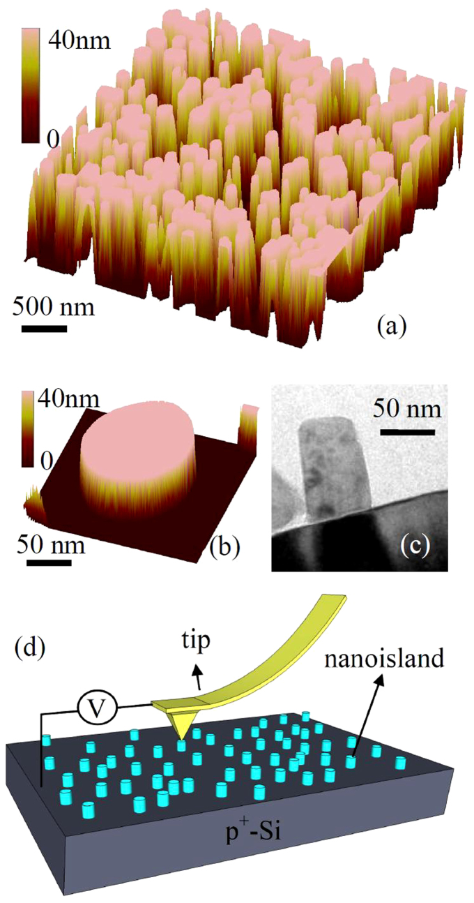
Fig. 1 (a) shows a three-dimensional (3D) AFM image of ZnO nanoislands. Fig. 1 (b) and (c) show the 3D AFM and transmission electron microscopy (TEM) images of one nanoisland, respectively. Although AFM characterization results show that the ZnO nanoislands are large and connected due to tip effect18, the TEM image in Fig. 1 (c) indicates that the diameter of the nano-island is about 50 nm. Detailed analysis of cross sectional scanning electron microscopy (SEM) images also showed that the diameter of the ZnO nanoislands is between 10 nm and 60 nm and these islands are discrete17. In this experiment, we selected nanoislands with a diameter of around 30 nm and a height of about 40 nm. Fig. 1 (d) shows the schematic of ZnO nanoislands on Si and a C-AFM tip used for measurements.
Figure 1.
(a) 3D AFM image of the ZnO nanoislands; (b) 3D AFM and (c) TEM images of one nanoisland; Excluding the AFM tip effect, these characterizations show that the nanoislands are discrete and having sizes between 10 and 60 nm. (d) Schematic of ZnO nanoislands and a C-AFM tip used for measurements.
Fig. 2 (a) shows the threshold-like I–V characteristics when the current compliance was set at 10 nA. During measurement, the voltage was swept according to the process as follows: (0) 0 ~ 10 V, (1) 5 ~ 0 V, (2) 0 ~ −5 V, (3) −5 V ~ 0 V, (4) 0 ~ 5 V. The current compliance was set at 5 nA for process (0), and 10 nA for process (1) ~ (4), respectively. During process (0), the ZnO nanoisland system was switched from high resistive state (HRS) to low resistive state (LRS) when the voltage reached 9 V. In process (1) and (2), the nanoisland was at LRS until −2.6 V where it was switched to HRS, which is corresponding to a LRS for negative reading bias. In process (3) and (4), the switching behavior is similar to that in process (1) and (2), while the switching point is 2.6 V. The switching power is lower than 25 nW, corresponding to the switching surface power density of only 1 × 10³ W/cm2 as the active cell area is considered. This is the lowest switching surface power density compared to that of any nanoscale resistive memory system reported to date3,6,19.When the current compliance was set at 100 nA ~ 10 μA after process (0) to (4), self-rectifying type of I–V characteristics were observed in the same ZnO nanoisland system with voltage sweeping between −10 V and 10 V, as shown in Fig. 2 (b). When the voltage swept back from 10 V to −10 V, the nanoisland system kept at LRS until −10 V, where the system was switched to HRS. The nanoisland system kept at HRS when the voltage swept from −10 V to 10 V before the voltage reached 6 V or 9 V, where the system was switched to LRS. Further increase of current compliance to be equal to or larger than 50 μA led to ordinary bipolar resistive switching phenomenon, as shown in Fig. 2 (c).
Figure 2.
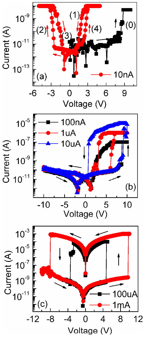
(a) threshold-like, (b) self-rectifying bipolar, and (c) ordinary bipolar I–V characteristics of a ZnO nanoisland at different current compliance. The nanoisland firstly underwent process (0) as indicated in (a), i.e., a voltage sweep from 0 to 10 V under a current compliance of 5 nA. Then the nanoisland underwent four voltage sweep processes sequentially (process (1): 5 to 0 V; process (2): 0 to −5 V; process (3): −5 to 0 V; process (4): 0 to 5 V) as illustrated in (a). Under the current compliance of 10 nA, 100 nA–10 μA, and 100 μA–1 mA, the voltage sweep processes resulted in three types of resistive switching (threshold-like, self-rectifying bipolar and ordinary bipolar) in (a), (b) and (c), respectively.
To further understand the threshold-like I–V characteristics, a voltage pulse of +2 V and −2 V was utilized to read the current of the ZnO nanoisland after process (1) to (4), respectively. The statistical results are shown in Fig. 3. When a pulse of +2 V was applied, the ZnO nanoisland was at LRS after process (1) and (4), while at HRS after process (2) and (3). On the contrary, when a pulse of −2 V was applied, the ZnO nanoisland stayed at HRS after process (1) and (4), while at LRS after process (2) and (3). These results indicate that both states can be kept after the power is shut down, which is bistable resistive switching behavior, while the resistance of the ZnO nanoisland depends on both the process that the nanoisland undergoes and the polarity of the reading voltage.
Figure 3. Statistic results of current reading at +2 V and −2 V after process (1) to (4), respectively when the current compliance was set at 10 nA.
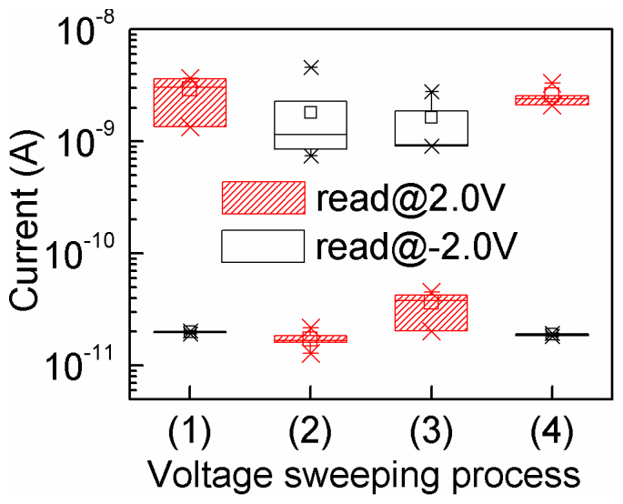
Both states can be kept after the power is shut down while the resistance of the ZnO nanoisland depends on both the process that the nanoisland undergoes and the polarity of the reading voltage. This suggests that the observed threshold-like I–V characteristics is a bistable resistive switching.
In order to study the threshold-like I–V characteristics in detail, the zoomed-in plots are shown in Fig. 4 (a) for processes (1) and (2) with the current ranging between −0.02 nA and 0.04 nA, and in Fig. 4 (b) for processes (3) and (4) with the current ranging between −0.04 nA and 0.04 nA. As seen in Fig. 4 (a), the I–V characteristics is the ordinary one for a forward-biased diode for process (1) and (2), while it is the ordinary one for the reversed diode for process (3) and (4), as shown in Fig. 4 (b). The I–V characteristics of process (1) ~ (4) were repeatable only if the tip was kept on the ZnO nanoisland. Turn-on voltages ofV1 (1.1 V) andV2 (0.9 V) are observed for the two diodes, respectively. Breakdown characteristics of the diodes are also observed, which may be due to tunneling effect20.
Figure 4. Zoomed-in I–V characteristics of (a) for processes (1) and (2), and (b) for processes (3) and (4) under a current compliance of 10 nA.
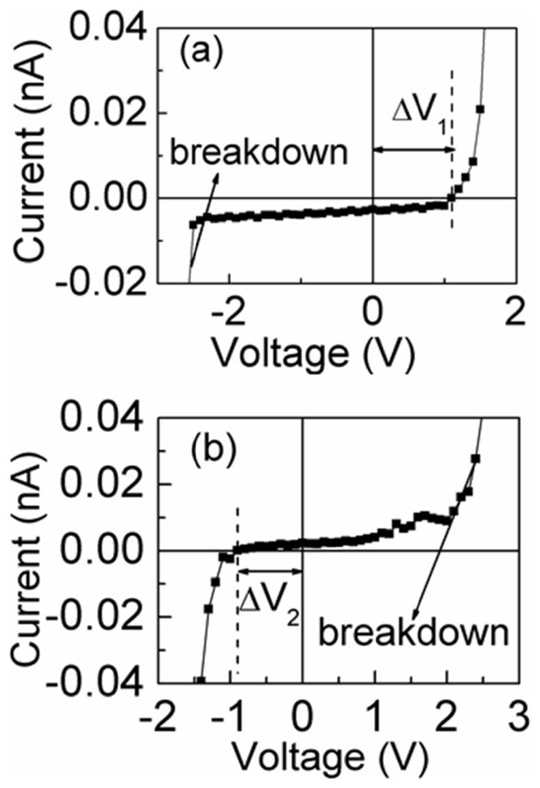
I–V characteristic in (a) shows the ordinary behavior for a forward-biased diode, while in (b) it is the one for a reversed-biased diode. The turn-on voltages are V1 (1.1 V) and V2 (0.9 V) for the forward-biased and reversed-biased diodes, respectively. Breakdown characteristics of the diodes are also evident.
To obtain the current distribution for the low resistive state of the ZnO nanoisland, C-AFM map measurements were performed. Fig. 5 (a) shows height image and Fig. 5 (b) and (c) show local current distribution images for LRS and HRS of ZnO nanoisland under the current compliance of 10 nA ~ 10 μA, respectively. It is evident that the current at LRS is not distributed locally in the nanoisland in contrast to the conducting filament case17.
Figure 5.
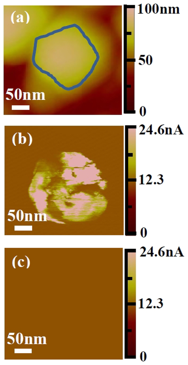
(a) AFM topographical image recorded in air on a ZnO nanoisland on Si substrate. Local current distributions (C-AFM) image for (b) LRS and (c) HRS of the ZnO nanoisland. The current is not distributed locally in the nanoisland and no conducting filaments are formed at LRS and no current can be observed for HRS at the same current bar of 24.6 nA.
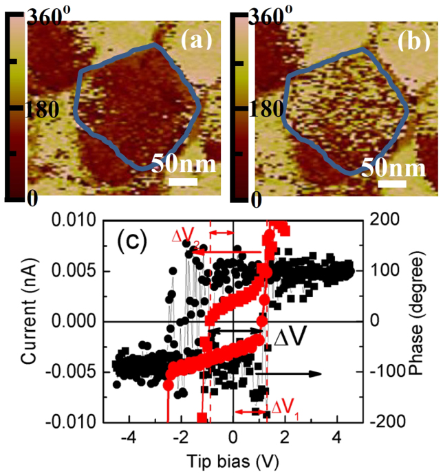
Fig. 6 (a) and (b) show the piezoresponse force microscopy (PFM) phase images in vertical mode for the nanoisland after process (2) and (4), respectively. Dark and light regions correspond to the two opposite build-in electric field directions. After process (2), the ZnO nanoisland has a build-in electric field oriented away from the substrate. However, the nanoisland has a build-in electric field oriented towards the substrate after process (4). These results are repeatable for both the same island in different cycles and different ZnO nanoislands. Fig. 6 (c) shows the PFM hysteresis phase loop together with zoomed-in I–V characteristics. The voltage to induce phase change matches V1 (1.1 V) and V2 (0.9 V) very well. These built-in fields correlate with the observed turn-on voltages.
Figure 6.
PFM images of ZnO nanoisland in vertical contrast at room temperature for (a) after process (2), and (b) after process (4). (c) PFM hysteresis phase loop (right axis) and further zoomed-in I–V characteristics (left axis). The overall electric fields in the ZnO nanoisland are opposite after process (2) and (4), respectively, which corresponds to the formation of C-AFM/ZnO Schottky diode and n-ZnO/Si substrate diode under these conditions. The smallest voltage window (ΔV) to induce phase change matches V1 (1.1 V) and V2 (−0.9 V) very well, which is a direct evidence of the need of reduce the built-in field to turn on each diode. These built-in fields correlate with the observed turn-on voltages.
Discussion
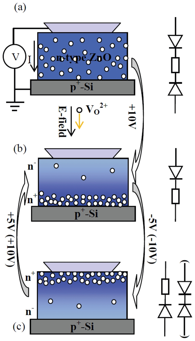
The I–V characteristics shown in Fig. 4 can be explained by the schematic illustration shown in Fig. 7. In the initial state, the oxygen vacancies are uniformly distributed in the nanoisland. The nanoisland system can be modeled as being composed of one Schottky diode (between the C-AFM tip and nanoisland) and one p+-n diode connected back to back, in series with the semiconducting ZnO nanoisland with a resistor R as shown in Fig. 7 (a). During process (0), more oxygen vacancies are generated by the oxidation reaction of  21. At the same time, both the original and generated oxygen vacancies move towards the cathode (the substrate). Finally, the portion of the ZnO nanoisland near the cathode side is heavily doped with oxygen vacancies, which act as donors in ZnO22. Meanwhile, the portion of the ZnO nanoisland near the anode side (the C-AFM tip) becomes n−-type. As a result, the diode between the ZnO nanoisland and heavily doped p-type Si substrate becomes a tunnel diode consisting of p+-Si and n+-ZnO, which can be treated as a resistor23, as shown in Fig. 7 (a) and (b). During process (2), the tip is negatively biased. Oxygen vacancies move towards the C-AFM tip, converting ZnO near the C-AFM tip to be n+. The barrier between the ZnO nanoisland and C-AFM tip is thinner, which results in significant electron tunneling24,25. Therefore, the Schottky diode can be treated as a resistor in this case. At the same time, the diode between the substrate and ZnO nanoisland turns into a p+-n hetero-junction, as shown in Fig. 7 (b) and (c). During process (4), similar reaction occurs as in process (2). The mechanism is confirmed by the results of C-AFM shown in Fig. 5 (b) and (c).
Figure 7. Schematic illustration of switching mechanism of C-AFM tip/ZnO nanoisand/Si substrate resistive memory to explain the observed threshold-like and self-rectifying bipolar switching behavior.
(a) The initial state, showing that the nanoisland system can be modeled as being composed of one Schottky diode consisting of the C-AFM tip and nanoisland and one p+-n diode consisting of the Si substrate and ZnO nanoisland connected back to back, in series with the semiconducting ZnO nanoisland with a resistor R. (b) Conversion of p+-Si/n-ZnO rectifying junction to p+-Si/n+-ZnO tunnel junction as a result of diffusion of the oxygen vacancies after a voltage sweep from 0 V to +10 V. In this case, the p+-Si/n+-ZnO tunnel junction can be treated as a resistance and there is only one rectifying junction in the loop. (c) C-AFM tip/ZnO Schottky junction converts to Ohmic junction or keeps as Schottky junction depending on the current compliance as a result of diffusion of oxygen vacancies after the voltage sweep from 0 to −5 V or −10 V. The Schottky junction can be treated as a resistor at current compliance of 10 nA because of current tunneling through the very thin barrier. Current self-rectifying resistive switching occurs when the Schottky diode can be treated as a rectifying diode rather than a resistor, as shown in the bracket in (c), in which tunneling current of 10 nA no longer represents LRS because of higher current value after the voltage sweeping from 0 to 10 V. At the same time, the p+-n+ tunneling diode between the substrate and ZnO nanoisland turns into a p+-n heterojunction. During the voltage sweep from 0 to 5 V or 10 V as indicated by an arrow pointing from (c) to (b), similar reaction occurs as in voltage sweep of 0 ~ −5 V or −10 V.
Under the current compliance of between 100 nA and 10 μA, the system can still be treated as a Schottky diode in series to one resistor, as shown in Fig. 7 (b), because oxygen vacancies move towards the substrate after operation of voltage sweeping from 0 to 10 V. The reason for the diode to be treated as a resistor is that heavily oxygen-vacancy-doped ZnO/p+-Si junction is a tunnel diode. After operation of voltage sweeping from 0 to −10 V, the diode between ZnO and p+-Si can now be treated as a regular heterojunction because oxygen vacancies move back to and gather around the C-AFM tip side again. In the meantime, the barrier between the C-AFM tip and heavily oxygen-vacancy-doped ZnO gives rise to Schottky characteristics because the C-AFM tip is mainly composed of Co, which has high work function of 5.0 eV26. In this case, the system can be depicted as one diode and one Schottky diode connected back to back, as shown in the bracket part of Fig. 7 (c). In other words, the asymmetric structure of C-AFM tip/ZnO and p+-Si/ZnO can be utilized to explain the self-rectifying type of I–V characteristics shown in Fig. 2 (b). Similar self-rectifying effect at LRS was also observed in the structures of Ni/HfOx/n+-Si27, Au/ZrO2:nc-Au/n+-Si28 by other researchers.
As the current compliance is further elevated to 50 μA or higher, the oxygen vacancies will form some conducting filaments along the boundary (side wall) of the island because of high electric field. The usual bipolar resistive switching behavior is controlled by the re-formation and rupture of the conducting filaments consisting of oxygen vacancies, as proven by C-AFM and HSR-AES results reported previously17.
The time needed to move the oxygen vacancies through the nanoisland towards the cathode can be estimated at very high electric field according to29
where L is the height of the ZnO nanoisland.  is the oxygen mobility,
  is the characteristic field for oxygen vacancy in ZnO lattice, which is about 0.5 MV/cm at 300 K and 1.3 MV/cm at 800 K.
  is the average electric field. kB, T, q are the Boltzmann constant, temperature and charge of oxygen vacancy, respectively. a = 0.52 nm30 is the lattice constant of c-axis for ZnO. f = 1013 Hz is the attempt-to-escape frequency, which is usually accepted to be the lattice vibration frequency31.
  32 is the migration energy of oxygen vacancy along c direction in ZnO. When the electric fields are well below the characteristics field, the time can be estimated by
  . Fig. 8 shows the estimated results. The estimated time vs. absolute value of SET and RESET voltage at room temperature shown in Fig. 8 (a) indicates that the time decreases greatly with the increase of the SET and RESET voltages. However, the field enhanced ion mobility is still so low that the SET and RESET time are much longer than the experiment results, which indicates that thermal enhanced ion mobility play main role. The local temperature of the nanoisland increases with the applied voltage due to the Joule heating effect29. For the SET and RESET voltage of 7 V, the estimated time is shortening with the increase of the local temperature, as shown in Fig. 8 (b). According to the results of Menzel et al, the local temperature can be as high as 800 K at the voltage of 6 V. At the local temperature of 800 K, the SET and RESET time is 0.28 ms, which is comparable to the voltage sweeping speed.
Figure 8. The estimated time needed to move oxygen vacancies through the nanoisland.
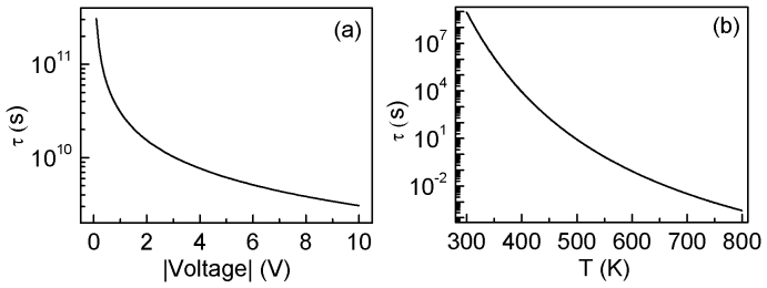
(a) The estimated time vs. absolute value of SET or RESET voltage at room temperature; (b) the estimated time vs. local temperature at SET or RESET voltage of 7 V. At room temperature, the estimated time decreases greatly with the increase of SET or RESET voltage. For the SET or RESET voltage of 7 V, the time is shortening with the increase of temperature. At the temperature of 800 K, the time is 0.28 ms.
PFM results indicate that the overall electric fields in the ZnO nanoisland are opposite after process (2) and (4), respectively, which corresponds to the formation of C-AFM/ZnO Schottky diode and n-ZnO/Si substrate diode under these conditions, i.e. the migration of oxygen vacancies in different direction at different voltage sweep process in ZnO nanoisland. PFM experiments validate the effect of the movement of oxygen vacancies in C-AFM tip/ZnO nanoisland/Si-substrate resistive memory on the switching behavior.
In summary, multimode resistive switching phenomena with threshold-like, self-rectifying, and ordinary bipolar I–V characteristics were observed in single self-assembled ZnO nanoisland of about 30 nm in diameter on p+-Si substrate using C-AFM tip as top contact when applying different current compliances. I–V characteristics, C-AFM, PFM results show that the threshold-like and self-rectifying types of switching are controlled by movement of oxygen vacancies in ZnO nanoisland while ordinary bipolar resistive switching is controlled by formation and rupture of conducting nanofilaments consisting of oxygen vacancies. The switching power density of only 1 × 10³ W/cm2 was demonstrated. This research suggests that high-density, low-power, and multimode resistive memory arrays are feasible by integrating ultra-small ZnO nanoislands on Si.
Methods
Self-assembled ZnO single-crystalline nanoislands were grown on pre-cleaned p+-Si (100) substrates at 350°C in a radio frequency plasma-assisted SVTA ZnO MBE system. The growth details can be found elsewhere17. Structural properties of ZnO nanoislands were characterized using TEM and AFM. The cross-sectional TEM specimens were prepared by a typical focus ion beam method, using FEI Quanta 3D FEG dual-beam instrument. The original sample surface was protected by a carbon layer and an electron beam-induced Pt layer formed by using Pt gas injection system and an electron beam. The TEM images were obtained using FEI CM-20 TEM operated at 200 kV with a LaB6 filament. FIB and TEM experiments were performed in the laboratory for Electron and X-ray instrumentation at UCI. Electrical characterizations of discrete ZnO nanoislands were carried out in air under controlled temperature (~22°C) and humidity (~12%) with an Agilent 4155C semiconductor parameter analyzer by applying sweeping voltages to obtain I–V characteristics at short integration time corresponding to the sweep rate of 6.4 ms/V for the nanoisland memory system, in which a Cr/Co coated C-AFM tip (MESP) with apex curvature radius of 20–50 nm was used as the top contact and the substrate as the bottom contact. The detail for equipment connection can be found elsewhere17. AFM, C-AFM and PFM measurements were performed in air under controlled temperature (~22°C) and humidity (~12%) using a Veeco Dimension Icon AFM equipment (Nanoscope v8.10) with C-AFM and PFM capabilities. The C-AFM images were measured under contact mode while AFM and PFM images were obtained under tapping mode. The amplitude and frequency of the ac voltage applied on the Cr/Co coated Si tip during PFM phase images measurements were −10 V ~ 10 V and 2 kHz, respectively. The hysteresis phase loop was acquired by scanning an axial dc bias from −10 to 10 V.
Author Contributions
J.Q. and J.L. conceived and designed the experiment. J.Q. and M.O. carried out the experiments. J.Z. performed the FIB and TEM experiment. J.Q. and J.L. wrote the manuscript and other co-authors commented the paper.
Acknowledgments
The authors acknowledge the financial and program support of the DARPA/Defense Microelectronics Activity (DMEA) under agreement number H94003-10-2-1003 (3D Electronics), the Microelectronics Advanced Research Corporation (MARCO) and its Focus Center on Function Engineered Nano Architectonics (FENA), National Natural Science Foundation of China (No. 50902065), the Fundamental Research Funds for the Central Universities (No. lzujbky-2013-33) and Open Project of Key Laboratory for Magnetism and Magnetic Materials of the Ministry of Education, Lanzhou University (No. LZUMMM2013008). We thank Applied Technology Training Center at San Bernardino Community College District for the AFM equipment.
References
- Meijer G. I. Who wins the nonvolatile memory race? Science 319, 1625–1626 (2008). [DOI] [PubMed] [Google Scholar]
- Asamitsu A., Tomioka Y., Kuwahara H. & Tokura Y. Current switching of resistive states in magneto resistive manganites. Nature 388, 50–52 (1997). [Google Scholar]
- Waser R. & Aono M. Nanoionics-based resistive switching memories. Nat. Mater. 6, 833–840 (2007). [DOI] [PubMed] [Google Scholar]
- Lee M. J. et al. Two series oxide resistors applicable to high speed and high density nonvolatile memory. Adv. Mater. 19, 3919–3923 (2007). [Google Scholar]
- Moreno C. et al. Reversible resistive switching and multilevel recording in La0.7Sr0.3MnO3 thin films for low cost nonvolatile memories. Nano Lett. 10, 3828–3835 (2010). [DOI] [PubMed] [Google Scholar]
- Park W. I. et al. Self-assembly-induced formation of high-density silicon oxide memristor nanostructures on graphene and metal electrodes. Nano Lett. 12, 1235–1240 (2012). [DOI] [PubMed] [Google Scholar]
- Kim M. J. et al. Low power operating bipolar TMO ReRAM for sub 10 nm era. IEDM Tech. Dig. 19.3.1–19.3.4 (2010). [Google Scholar]
- Ho C. H. et al. 9 nm half-pitch functional resistive memory cell with < 1 μA programming current using thermally oxidized sub-stoichiometric WOx film. IEDM Tech. Dig. 19.1.1–19.1.4 (2010). [Google Scholar]
- Park J. et al. Quantized conductive filament formed by limited Cu source in sub-5 nm era. IEDM Tech. Dig. 3.7.1–3.7.4 (2011). [Google Scholar]
- Weitz R. T., Walter A., Engl R., Sezi R. & Dehm C. New charge-transfer salts for reversible resistive memory switching. Nano. Lett. 6, 2810–2813 (2006). [DOI] [PubMed] [Google Scholar]
- Nagashima K. et al. Resistive switching multistate nonvolatile memory effects in a single cobalt oxide nanowire. Nano. Lett. 10, 1359–1363 (2010). [DOI] [PubMed] [Google Scholar]
- Jo S. H. & Lu W. CMOS compatible nanoscale nonvolatile resistance switching memory. Nano Lett. 8, 392–397 (2008). [DOI] [PubMed] [Google Scholar]
- Wang J., Sun B., Gao F. & Greenham N. C. Memristive devices based on solution-processed ZnO nanocrystals. Phys. Stat. Sol. A 207, 484–487 (2010). [Google Scholar]
- Kim T. H. et al. Nanoparticle assemblies as memristors. Nano Lett. 9, 2229–2233 (2009). [DOI] [PubMed] [Google Scholar]
- Hueso L. E., Bergenti I., Riminucci A., Zhan Y. & Dediu V. Multipurpose magnetic organic hybrid devices. Adv. Mater. 19, 2639–2642 (2007). [Google Scholar]
- Nardi F. et al. Control of filament size and reduction of reset current below 10 μA in NiO resistance switching memories. Solid State Electron. 58, 42–47 (2011). [Google Scholar]
- Qi J. et al. Resistive switching in single epitaxial ZnO nanoislands. ACS Nano 6, 1051–1058 (2012). [DOI] [PubMed] [Google Scholar]
- Ramirez-Aguilar K. A. & Rowlen K. L. Tip characterization from AFM images of nanometric spherical particles. Langmuir 14, 2562–2566 (1998). [Google Scholar]
- Nagashima K. et al. Intrinsic mechanisms of memristive switching. Nano Lett. 11, 2114–2118 (2011). [DOI] [PubMed] [Google Scholar]
- Sze S. M. & Ng K. K. Physics of Semiconductor Devices (Wiley, New Jersey, 2007) 102–104. [Google Scholar]
- Waser R., Dittmann R., Staikov G. & Szot K. Redox-based resistive switching memories-nanoionic mechanisms, prospects, and challenges. Adv. Mater. 21, 2632–2663 (2009). [DOI] [PubMed] [Google Scholar]
- Zhang S. B., Wei S.-H. & Zunger A. Intrinsic n-type versus p-type doping asymmetry and the defect physics of ZnO. Phys. Rev. B 63, 075205-1–075205-7 (2001). [Google Scholar]
- Talley H. E. Physical Principles of Semiconductor Devices (Ames, 1976) 205–208. [Google Scholar]
- Zhang Z. Y. et al. Quantitative analysis of current–voltage characteristics of semiconducting nanowires: decoupling of contact effects. Adv. Fun. Mater. 17, 2478–2489 (2007). [Google Scholar]
- Appenzeller J., Radosavljevic M., Knoch J. & Avouris Ph. Tunneling versus thermionic emission in one-dimensional semiconductors. Phys. Rev. Lett. 92, 048301-1–048301-4 (2004). [DOI] [PubMed] [Google Scholar]
- Sze S. M. & Ng K. K. Physics of Semiconductor Devices (Wiley, New Jersey, 2007) 137–137. [Google Scholar]
- Tran X. A. et al. Self-rectifying and forming-free unipolar HfOx based-high performance RRAM built by fab-avaialbe materials. IEDM Tech. Dig. 31.2.1–31.2.4 (2011). [Google Scholar]
- Zuo Q. et al. Self-rectifying effect in gold nanocrystal-embedded zirconium oxide resistive memory. J. Appl. Phys. 106, 073724-1–073724-5 (2009). [Google Scholar]
- Menzel S. et al. Origin of the ultra-nonlinear switching kinetics in oxide-based resistive switches. Adv. Funct. Mater. 21, 4487–4492 (2011). [Google Scholar]
- Ozgur U. et al. A comprehensive review of ZnO materials and devices. J. Appl. Phys. 98, 041301-1–041301-103 (2005). [Google Scholar]
- Studenikin S. A., Golego N. & Cocivera M. Optical and electrical properties of undopedZnO films growth by spray pyrolysis of zinc nitrate solution. J. Appl. Phys. 83, 2104–2111 (1998). [Google Scholar]
- Tomlins G. W., Routbort J. L. & Mason T. O. Zinc self-diffusion, electrical properties, and defect structure of undoped, single crystal zinc oxide. J. Appl. Phys. 87, 117–123 (2000). [Google Scholar]


