Abstract
We demonstrate liquid crystal-on-organic field-effect transistor (LC-on-OFET) sensory devices that can perceptively sense ultralow level gas flows. The LC-on-OFET devices were fabricated by mounting LC molecules (4-cyano-4′-pentylbiphenyl – 5CB) on the polymer channel layer of OFET. Results showed that the presence of LC molecules on the channel layer resulted in enhanced drain currents due to a strong dipole effect of LC molecules. Upon applying low intensity nitrogen gas flows, the drain current was sensitively increased depending on the intensity and time of nitrogen flows. The present LC-on-OFET devices could detect extremely low level nitrogen flows (0.7 sccm–11 μl/s), which could not be felt by human skins, thanks to a synergy effect between collective behavior of LC molecules and charge-sensitive channel layer of OFET. The similar sensation was also achieved using the LC-on-OFET devices with a polymer film skin, suggesting viable practical applications of the present LC-on-OFET sensory devices.
Artificial sensation is of importance to help people who have a sensory disability problem and to develop humanoid-type robots, which can share a routine and difficult job of humans1,2,3,4,5. Of various kinds of sensations a tactile sensation is considered the most basic part because human brains, for example, should make quick decision on how to respond against physical (tactile) stimulations for self-protection and next actions6,7,8. In particular, sensing an extremely low intensity of physical stimulations is required to secure sufficient times for next responses. In addition, aftersensation phenomena (signal duration time after physical stimulation) are also required to get enough feedback times according to the intensity of stimulations for finding an accurate position on physical stimulations and for preparing follow-up measures9,10,11.
Considering above requirements for artificial tactile sensations with both low intensity touch sensing and aftersensation functions, conventional artificial sensory devices cannot afford to actually satisfy the criteria because they are basically operated by a direct pressing-touch with considerably high pressures and/or by a capacitance change after pressing (such as a touch panel for smart phones etc)12,13,14,15,16,17,18. Moreover, such conventional devices have been fabricated with inorganic semiconductors so that they do inherently lack of flexibility enough to apply for realistic artificial sensation skins in various applications including humanoid-robots. Hence, we need to invent an artificial tactile sensation device based on organic (plastic) electronics, which can provide flexible and conformable artificial tactile sensation devices in the future19,20,21.
In this work, as the first step toward realizing artificial tactile sensation devices based on organic electronics, we attempted to combine liquid crystal (LC) and organic field-effect transistor (OFET) technologies, leading to liquid crystal-on-organic field-effect transistor (LC-on-OFET) sensory devices. The main idea here is to exploit the property of LC molecules that have a strong dipole alignment in a liquid crystal state and undergo a collective molecular moving upon stimulation. This particular feature of LC molecules enables both generation of additional charge carriers in the organic (polymer) channel layer of OFET (due to the strong dipole effect of LC molecules) and aftersensation-like signal decay (due to the recovery of LC molecular orientations – not electrons): For example, the response time of conventional nematic LCs is about 1 ~ 10 ms in liquid crystal displays so that it may fall into a human action potential range (100–280 ms in overall; note that just ion movement is <5 ms in local ion channels) by control22,23,24. To prove the exact functioning of the present LC-on-OFET sensory devices upon considerably low external stimulations, we tried to apply nitrogen flows on top of the LC surface in the devices by controlling the applying time and intensity of nitrogen flows. To examine their possibility for practical applications, the nitrogen gas flows were also applied on the surface of a polymer film skin (to protect LC molecules) that is placed on top of the LC layer in the LC-on-OFET devices.
Results
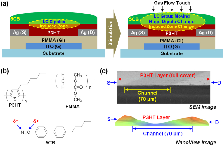
A brief operation principle for the LC-on-OFET sensory devices can be explained as four steps (see illustrations in Fig. 1a): (1) The presence of LC molecules, 4-cyano-4′-pentylbiphenyl (5CB), is expected to generate charges on the organic channel layer, poly(3-hexylthiophene) (P3HT), by the strong dipole effect of 5CB (dielectric constant = 11)25,26. (2) Upon stimulating a few 5CB molecules on the top part of the 5CB layer with a nitrogen gas flow, a group of adjacent 5CB molecules is considered to change their orientations by following the stimulated 5CB molecules owing to a particular collective behavior of LC molecules in ordered states. (3) Then the orientation change of 5CB molecules results in the variation of charges induced by the strong dipole of 5CB molecules. (4) Finally, this varied (affected) charge state in the channel (P3HT) layer influences on the drain current (ID) that flows between source and drain electrodes. In brief, the 5CB molecules act as a sensitizer for the nitrogen gas touch, while the P3HT layer plays a creation/amplification role of electrical signals induced by the orientation change of 5CB molecules. Here we need to pay our attention to the channel structure and shape (see images in Fig. 1b and Fig. S1), which indicates that the height of the P3HT layer is lower than the height of source/drain electrodes (we note that the P3HT layer was coated over the source/drain electrodes in the present OFET – see the scanning electron microscope (SEM) and NanoView images in Fig. 1c). This geometry implies that both the LC molecules on the surface of the P3HT layer and the LC-induced charged parts in the P3HT layer are actually affected by drain voltage (VD) between source (S) and drain (D) electrodes. The evidence for this scenario will be discussed again below.
Figure 1. Illustration for the device structure of LC-on-OFET sensory devices and their operation.
(a) Operation of the LC-on-OFET sensory devices upon nitrogen gas flow stimulation; (left) generation of charges in the P3HT layer by the strong dipoles of LC molecules, (right) change of the induced charges by the gas flow stimulation owing to the collective movement of LC molecules. (b) Materials used for the fabrication of the LC-on-OFET sensory devices. (c) SEM (top) and NanoView (bottom) images for the surface of the OFET device which is fully covered by the P3HT layer (note that a 60 nm-thick silver layer was additionally coated on the P3HT layer of the device for the NanoView measurement). ‘S' and ‘D' denote source and drain electrodes, respectively.
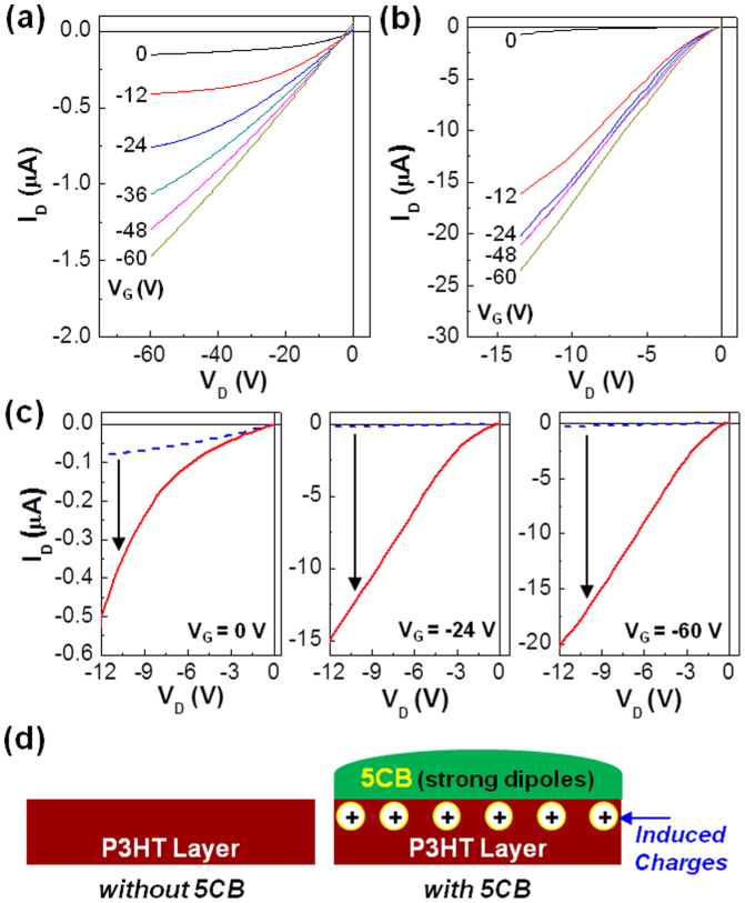
To prove above operation principle, we first investigated the nature of LC-on-OFET devices before the nitrogen gas stimulation. As shown in Fig. 2a, the OFET without the LC layer exhibited typical output and transfer curves with a hole mobility of 2 × 10⁻³ cm2/V·s and an on/off ratio of ~103 (note that this is one of the best performances for bottom gate and bottom S/D electrode type OFETs). Surprisingly, the drain current (ID) was significantly increased after placing the 5CB layer on the surface of the P3HT layer. Considering the enhanced ID in the output curve even at zero gate voltage (VG = 0 V) (see Fig. 2c left), it is expected that the 5CB layer might induce a positive charge in the channel (P3HT) layer because of strong dipole moments in 5CB molecules (see Fig. 2d)25,26. Interestingly, as shown in Fig. 2c (middle and right panels), the ID enhancement was strongly affected by the VG change. This result reflects that the present LC-on-OFET devices are sensitive to the VG change so that they can be controlled by varying VG. Here we note that no such transistor characteristics were measured for the device with only 5CB layer without the channel (P3HT) layer (see Fig. S2), which supports that the LC molecules themselves cannot transport such major charges, although an extremely low level ohmic current can be measured for most of dielectric materials (like a resistor for electrical circuits).
Figure 2. Output characteristics of devices.
(a) OFET device (without the LC layer), (b) LC-on-OFET sensory device, (c) comparison for the output curves of the OFET devices with and without the LC layer, (d) illustration for the generation of positive charges in the channel (P3HT) layer by the induction of the strong dipoles in the LC (5CB) molecules. The gate voltages (VG) for the operation of the OFET devices are given in each graph.
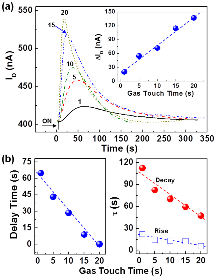
Using the properly working LC-on-OFET devices, we tried to examine whether they can respond to a low intensity nitrogen flow touch or not. For this examination we controlled the nitrogen flow rate as 33 μl/s (2 sccm), which is almost a lowest level that human skins can or cannot feel (though it may be slightly different from person to person). As shown in Fig. 3a, the ID signal (note that the minus (−) sign in the ID values was omitted) was noticeably increased upon applying 33 μl/s nitrogen flow for 1 s to the LC layer on the LC-on-OFET device. Interestingly, even after stopping the nitrogen flow (only 1 s duration), the ID signal was continuously increased and showed a maximum at around 64 s (see also Fig. 3b left). Moreover, the ID signal decay was measured to be much lower than the ID signal rise (see also Fig. 3b right). However, this trend was pronouncedly changed by increasing the applying time of nitrogen flow. As the nitrogen flow (gas touch) time increased, the delay time for reaching a maximum ID after stopping the nitrogen flow was remarkably reduced so that almost no delay was observed when the nitrogen flow time was 20 s (note that the longer the gas touch time, the higher the ID signal intensity). This result implies that the full orientation change of 5CB molecules upon external stimulation (nitrogen flow touch) may require at least 20 s in the present LC-on-OFET device structure, which can be ascribed to the influence of some 5CB molecules that are located relatively far from the active region affected by the electric field between the S/D electrodes (see Fig. 1a). Here we note that the response time of 5CB in the structure of liquid crystal displays could be as quick as <10 ms (as mentioned in the introduction section) because all 5CB molecules are well aligned and affected by an electric field between two electrodes22,23,24. As a result, both rise and decay time constants (τ), which were obtained by fitting with the ID – time (t) plot (Fig. 3a) based on a single exponential rise/decay equation (see the method part in detail)27,28, were gradually decreased as the gas flow touch time increased (Fig. 3b right). The discrepancy between rise and decay time constants can be attributed to whether a forced stimulation (initial gas flow touch) was applied or not.
Figure 3. Effect of nitrogen gas applying time.
(a) Change of drain current (ID) as a function of time in the LC-on-OFET sensory devices upon applying nitrogen gas flows to the LC surface, where the intensity of nitrogen gas flows was fixed as 33 μl/s (2 sccm) but the applying time was varied from 1 s to 20 s; Inset shows the change of maximum (peak) ID as a function of nitrogen gas flow applying time. (b) Change of delay time (left) and time constants (right) as a function of nitrogen gas flow applying time: The delay time is defined as the time (of the increasing ID trend) to reach a maximum (peak) value even after stopping the nitrogen gas flows, while the rise/decay time constants were obtained by fitting with a single exponential equation (see the details in the experimental part). Note that the minus (−) sign in ID was omitted to avoid crowding data display.
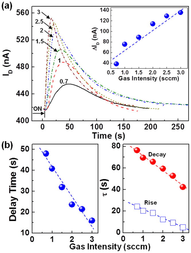
Next, we studied the influence of nitrogen flow strength (gas intensity) on the ID signal change in the LC-on-OFET devices by fixing the gas touch time as 15 s. As shown in Fig. 4a, the ID signal was also clearly measured even when the gas flow intensity was 0.7 sccm (11 μl/s) that is as low as human skins cannot feel at all. However, a time delay phenomenon was also observed as discussed in Fig. 3, and the time delay after stopping the nitrogen gas flow touch was noticeably decreased as the gas intensity increased. Hence the same explanation as discussed in Fig. 3 (the influence of some 5CB molecules that are weakly affected by an electric field) can be applied for this time delay according to the gas intensity (Fig. 4b). This explanation is also supported by the result that the ID signal intensity was almost proportionally increased as the gas intensity increased (see inset in Fig. 4a).
Figure 4. Effect of nitrogen gas intensity.
(a) Change of drain current (ID) as a function of time in the LC-on-OFET sensory devices upon applying nitrogen gas flows to the LC surface, where the intensity of nitrogen gas flows was varied from 11 μl/s (0.7 sccm) to ~50 μl/s (3 sccm) but the applying time was fixed as 15 s: Inset shows the change of maximum (peak) ID as a function of nitrogen gas flow intensity. (b) Change of delay time (left) and time constants (right) as a function of nitrogen gas flow intensity: The delay time is defined as the time (of the increasing ID trend) to reach a maximum (peak) value even after stopping the nitrogen gas flows, while the rise/decay time constants were obtained by fitting with a single exponential equation (see the details in the experimental part). Note that the minus (−) sign in ID was omitted to avoid crowding data display.
Discussion
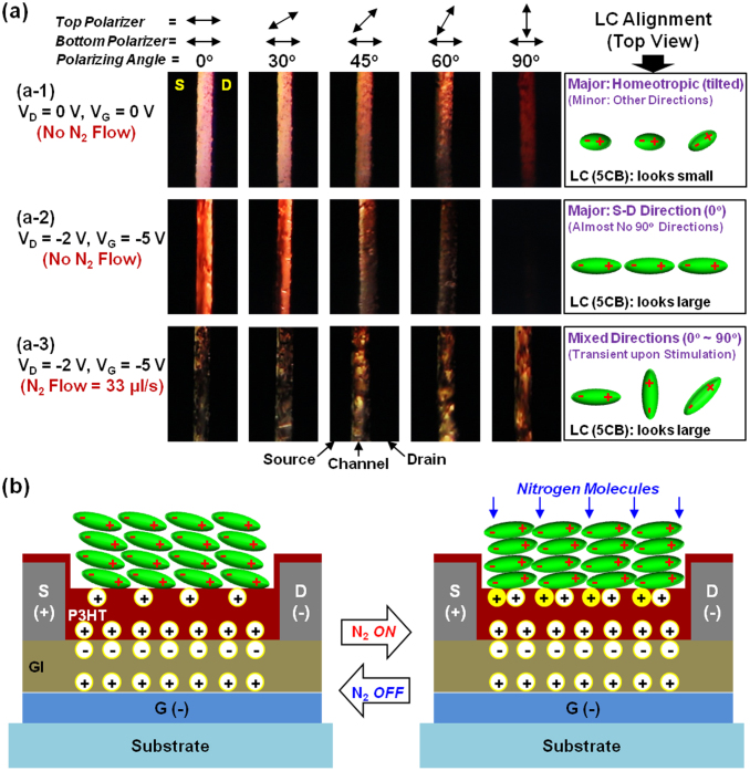
To understand the detailed sensing mechanism in the present LC-on-OFET devices, we investigated the alignment of 5CB molecules in the channel area by employing in-situ measurement of optical images during the nitrogen gas flow touch. When the LC (5CB) layer was just placed on top of the channel (P3HT) layer without applying any electric field, the highest optical transmittance in the channel area was measured when the two polarizers were in a parallel alignment but the transmittance was gradually decreased as the polarizing angle increased (see ‘a-1' case in Fig. 5a). This result informs that the 5CB molecules on the surface of the P3HT layer are expected to basically align in a homeotropic geometry owing to the hexyl groups in the P3HT surface29,30,31. However, they might be tilted with some angles from the vertical axis of homeotropic alignment because the channel was not completely dark in a cross-polarizing condition (see ‘top view' in the ‘a-1' case). Interestingly, when the electric field was applied to turn on the present p-type OFET (VD = −2 V and VG = −5 V), almost no light was measured in the channel area under cross-polarizing condition, even though a bright channel area was measured under the linear-polarizing condition. This result supports that most of the 5CB molecules do almost perfectly align in the direction parallel to the channel length (S-to-D direction) because of the applied electric fields (see ‘a-2' case). Considering the VD and VG values (negative electric fields), the negative poles in the 5CB molecules are expected to head for the source electrode and tilt toward the surface of the P3HT layer (see Fig. 5b left) because a strong hole current was measured by the presence of the 5CB molecules on the P3HT surface (see Fig. 2 and Fig. S3). Upon applying the low intensity nitrogen gas flow (33 μl/s) to the surface of the LC layer (under applied electric fields of VD = −2 V and VG = −5 V), the optical transmittance in the channel area was dramatically changed and fluctuated randomly irrespective of the polarizing angles (see ‘a-3' case in Fig. 5a). This indicates that the alignment of 5CB molecules was significantly affected by the low intensity nitrogen gas flow touch and the alignment direction was hugely changed from the original orientation as in the a-2 case. Here we need to pay attention to the (negatively) increased ID by the nitrogen gas flow touch (see also Figs. 3 and 4), which indicates generation of additional positive charges in the P3HT layer. This fact supports that the negative dipole parts in the 5CB molecules might be much closer to the surface of the P3HT layer by the nitrogen gas flow touch as ideally illustrated in Fig. 5b right (though the 5CB orientation on the surface of the P3HT layer was quite random and mixed as illustrated in the right part (top view) of ‘a-3' in Fig. 5a).
Figure 5. Understanding of mechanism for LC-on-OFET sensory devices.
(a) Optical microscope images focused on the channel parts in the LC-on-OFET devices (note that two polarizers were used to observe the LC alignment changes); (a-1) no electric fields and no nitrogen gas flow touch, (a-2) applying electric fields but no nitrogen gas flow touch, (a-3) applying both electric fields and nitrogen gas flow touch. The LC alignment (top view) is given schematically on the far right part for each case, where the (top view) size of LC (5CB) looks small or large depending on the LC alignment. (b) Illustration for the mechanism proposed here on the amplification of the ID signals by the nitrogen gas flow touch: ‘GI' and ‘G' denote the gate insulator (PMMA) and the gate electrode (ITO), respectively. The negative (−) and positive (+) dipoles in the LC (5CB) molecules are explained in Fig. 1.
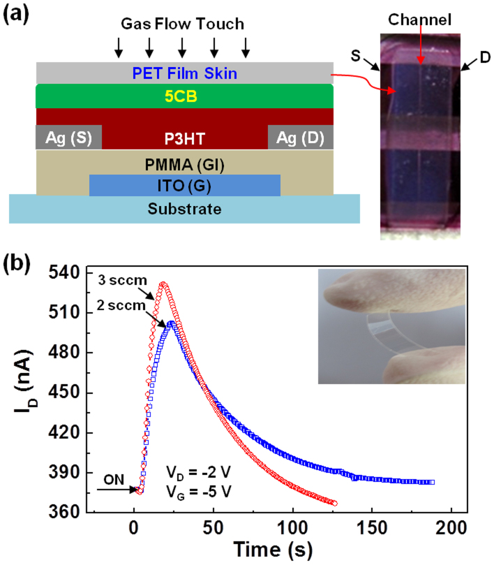
Finally, we briefly examined whether the similar sensing is possible when the LC layer was covered by a thin protective film skin, because the liquid-like LC layer on the P3HT layer is directly open to air so that it could be extremely vulnerable to external physical touches leading to destruction of the LC layer. As a protective film, we used a poly(ethylene terephthalate) (PET) film (thickness = 100 μm) because it is widely used for touch panels and flexible substrates in applications of smart phones etc. As shown in Fig. 6a, the PET film was placed on the LC layer in the LC-on-OFET devices and covered whole part of the channel area (see photograph on the right). When the nitrogen gas flow was applied on the surface of the PET skin, the ID was noticeably increased as shown in Fig. 6b. Just after turning off the nitrogen gas flow, the ID was decreased as similarly observed for the LC-on-OFET devices without the PET skin (see Figs. 3 and 4). In addition, the ID change (rise and decay) was different when the gas flow intensity was changed. This brief result supports that the present LC-on-OFET devices can be applicable for actual applications.
Figure 6. LC-on-OFET sensory devices with a thin PET film skin (thickness = 100 μm).
(a) Device structure (left) and photograph (photograph - top view). (b) Change of drain current (ID) as a function of time upon applying nitrogen gas flows to the surface of the PET skin placed on the LC (5CB) layer (The nitrogen gas applying time was fixed as 15 s). Note that the minus (−) sign in ID was omitted to avoid crowding data display. The inset photograph shows the PET film used as the skin layer, which is bendable and flexible.
In summary, we have fabricated LC-on-OFET sensory devices by forming the LC (5CB) layer on the surface of the channel (P3HT) layer that does also cover the source/drain (Ag) electrodes and the gate insulating layer in the OFET device. The drain current in the OFET devices was considerably enhanced by just placing the 5CB layer and then further amplified by applying gate voltages. When a nitrogen gas flow touched the 5CB layer in the LC-on-OFET sensory devices, the drain current was significantly increased, depending on the time and intensity of the applied nitrogen gas flows, owing to the dipole reorientation by the collective movement of 5CB molecules. In particular, the present LC-on-OFET sensory devices could sense ultralow-level nitrogen gas flows which cannot be felt by human skins. Achieving such high sensitivity of ultralow-level gas flows has been assigned to the collective behavior of LC molecules (i.e., many neighboring LC molecules move by just one stimulated LC molecule), which does sensitively affect the generation and variation of local dipoles in the channel layer of the OFET devices. Finally, similar drain current changes upon low intensity gas stimulations were measured for the LC-on-OFET devices with the PET skin, which supports possible practical applications of the present LC-on-OFET sensory devices.
Methods
Materials and device fabrication
The P3HT polymer (weight-average molecular weight = 70 kDa, polydispersity index = 1.8, regioregularity = 96%) was purchased from Rieke Metals, while poly(methyl methacrylate) (PMMA, weight-average molecular weight = 120 kDa, polydispersity index = 2.2) was supplied from Sigma-Aldrich. 5CB (purity = 98%) was used as received from Sigma-Aldrich. To fabricate LC-on-OFET devices, indium-tin oxide (ITO)-coated glass substrates were patterned to have 12 mm × 1 mm ITO stripes (as a gate electrode) and cleaned with acetone and isopropyl alcohol. After treating the patterned ITO-glass substrates with an ultraviolet-ozone (28 mW/cm2) for 20 min, the PMMA layers (thickness = 450 nm) were spin-coated on top of the ITO-glass substrates and soft-baked at 90°C for 60 min. Then silver (Ag) S/D electrodes were deposited on the PMMA layer through a shadow mask by employing a resistive evaporation technique in a vacuum chamber. After taking out the Ag-deposited substrates from the vacuum chamber, the P3HT layers were spin-coated on the Ag-deposited substrates (see Fig. 1a), followed by soft-baking at 60°C for 15 min. A close inspection showed that the P3HT layers did well cover both the channel part and the S/D electrodes. Finally, the LC-on-OFET sensory devices were completed by placing the 5CB layers on top of the P3HT layer. In addition, the LC-on-OFET devices with the PET skin were constructed by placing the PET film (thickness = 100 μm) on the 5CB layer in the devices.
Measurements and fitting
The surface and cross-section of the OFET devices were examined using a field-emission scanning electron microscope (FE-SEM, S-4800, HITACHI). A NanoView system (NV-E1000, NanoSystem) with a light source (Halogen 100 W, wavelength = 600 nm) was used to measure the surface profiles of the channel area including the S/D electrode parts. To prevent distorted optical (NanoView) images owing to the polymeric layers with an optical transparency, a thin Ag layer (thickness = 60 nm) was deposited on the surface of the P3HT layer in the OFET devices. The transistor characteristics were measured using a semiconductor parameter analyzer (4200CS, Keithley). To measure the ID signals from the LC-on-OFET devices upon applying nitrogen flows, the LC-on-OFET devices were mounted inside a specialized tactile sensor measurement system that is equipped with a probe station (PS-CPSN2, MODU-SYSTEMS), a polarized optical microscope unit (FPG-30.2-4.3, CVI Melles-Griot), a micro gas control unit (TSC-210, NF System) and an external controller (KRO-4000S, NF System). The rise and decay time constants (τ) for the ID signals were obtained by fitting with a single exponential equation, ID = ID0 + A·e(−t/τ), where ID0, A and t are an initial drain current, a proportional constant and a measurement time, respectively.
Author Contributions
Y.K. designed this work and supervised whole experimental processes; J.S.(main), S.P. and S.N. carried out all experiments and setup of measurement systems; H.K. helped with discussion for each step; Y.K. and H.K. wrote this manuscript and J.S. contributed to the editing of each section of final version.
Supplementary Material
Supplementary Information
Figure S4
Acknowledgments
This work was financially supported by Korean Government grants (Basic Research Laboratory Program_2011-0020264, Pioneer Research Center Program_2012-0001262, Basic Science Research Program_2009-0093819, NRF_2012R1A1B3000523, NRF_2012K1A3A1A09027883, NRF_2013M4A1039332) and Kyungpook National University Research Fund (2013).
References
- Gasson M., Hutt B., Goodhew I., Kyberd P. & Warwick K. Invasive neural prosthesis for neural signal detection and nerve stimulation. Int. J. Adapt. Control Signal Process 19, 365–375 (2005). [Google Scholar]
- Matsumoto S., Ishikawa A., Kume H., Takeuchi T. & Homma Y. Near infrared spectroscopy study of the central nervous activity during artificial changes in bladder sensation in men. Int. J. Urol. 16, 760–764 (2009). [DOI] [PubMed] [Google Scholar]
- Yoshida E. et al. Pivoting based manipulation by a humanoid robot. Auton Robot 28, 77–88 (2010). [Google Scholar]
- Hauser K. & Ng-Thow-Hing V. Randomized multi-modal motion planning for a humanoid robot manipulation task. Int. J. Robot. Res. 30, 678–698 (2011). [Google Scholar]
- Christensen H. et al. Are changes in sensory disability, reaction time, and grip strength associated with changes in memory and crystallized intelligence? Gerontology 46, 276–292 (2000). [DOI] [PubMed] [Google Scholar]
- Ptito M. et al. TMS of the occipital cortex induces tactile sensations in the fingers of blind braille readers. Exp. Brain. Res. 184, 193–200 (2008). [DOI] [PubMed] [Google Scholar]
- Miyaoka T., Mano T. & Ohka M. Mechanisms of fine-surface texture discrimination in human tactile sensation. J. Acoust. Soc. Am. 105, 485–2492 (1999). [DOI] [PubMed] [Google Scholar]
- Torebjörk H. E. & Hallin R. G. Perceptual changes accompanying controlled preferential blocking of A and C fibre responses in intact human skin nerves. Exp. Brain. Res. 16, 321–332 (1973). [DOI] [PubMed] [Google Scholar]
- Heller M. A. Tactile retention: Reading with the skin. Percept. Psychophys. 27, 125–130 (1980). [Google Scholar]
- Van Erp J. B. F., Groen E. L., Bos J. E. & Van Veen H. A. H. C. A tactile cockpit instrument supports the control of self-motion during spatial disorientation. Hum. Factors 48, 219–228 (2006). [DOI] [PubMed] [Google Scholar]
- Felsby S., Nielsen J., Nielsen l. & Jensen T. S. NMDA receptor blockade in chronic neuropathic pain: a comparison of ketamine and magnesium chloride. Pain 64, 283–291 (1995). [DOI] [PubMed] [Google Scholar]
- Cotton D. P. J., Graz I. M. & Lacour S. P. A multifunctional capacitive sensor for stretchable electronic skins. IEEE Sens. J. 9, 2008–2009 (2009). [Google Scholar]
- Adami A., Dahiya R. S., Collini C., Cattin D. & Lorenzelli L. POSFET touch sensor with CMOS integrated signal conditioning electronics. Sensor. Actuat. A-Phys. 188, 75–81 (2012). [Google Scholar]
- Hsieh T. et al. Application of in-cell touch sensor using photo-leakage current in dual gate a-InGaZnO thin-film transistors. Appl. Phys. Lett. 101, 212104 (2012). [Google Scholar]
- Turner A. P. F. Biosensors: sense and sensibility. Chem. Soc. Rev. 42, 3184–3196 (2013). [DOI] [PubMed] [Google Scholar]
- Kim S. et al. A highly sensitive capacitive touch sensor integrated on a thin-film-encapsulated active-matrix OLED for ultrathin displays. IEEE T. Electron. Dev. 58, 3609–3615 (2011). [Google Scholar]
- Zhao S., Li Y. & Liu C. A tri-axial touch sensor with direct silicon to PC-board packaging. Sensor. Actuat. A-Phys. 170, 90–99 (2011). [Google Scholar]
- Kimoto A. & Shida K. A new touch sensor for material discrimination and detection of thickness and hardness. Sensor. Actuat. A-Phys. 141, 238–244 (2008). [Google Scholar]
- Choi M. C., Kim Y. K. & Ha C. S. Polymers for flexible displays: From material selection to device applications. Prog. Polym. Sci. 33, 581–630 (2008). [Google Scholar]
- Ji Y. et al. Stable switching characteristics of organic nonvolatile memory on a bent flexible substrate. Adv. Mater. 22, 3071–3075 (2010). [DOI] [PubMed] [Google Scholar]
- Fujisaki Y. et al. Air-stable n-type organic thin-film transistor array and high gain complementary inverter on flexible substrate. Appl. Phys. Lett. 97, 133303 (2010). [Google Scholar]
- Zhu J., Lu J., Qiang J., Zhong E.-W. & Ye Z.-C. 1D/2D switchable grating based on field-induced polymer stabilized blue phase liquid crystal. Appl. Phys. Lett. 111, 033101 (2012). [Google Scholar]
- Shimoda Y., Ozaki M. & Yoshino K. Electric field tuning of a stop band in a reflection spectrum of synthetic opal infiltrated with nematic liquid crystal. Appl. Phys. Lett. 79, 3627–3629 (2001). [Google Scholar]
- Konshina E. A., Vakulin D. A., Ivanova N. L., Gavrish E. O. & Vasil'ev V. N. Optical response from dual-frequency hybrid-aligned nematic liquid crystal cells. Tech. Phys. 57, 644–648 (2012). [Google Scholar]
- Hisakado Y., Kikuchi H., Nagamura T. & Kajiyama T. Large electro-optic kerr effect in polymer-stabilized liquid-crystalline blue phases. Adv. Mater. 17, 96–98 (2005). [Google Scholar]
- Kędziora P. & Jadżyn J. Dipole-dipole association of mesogenic molecules in solution. Liq. Cryst. 8, 445–450 (1990). [Google Scholar]
- Nam S. H., Kim H. J., Degenaar P., Ha C.-S. & Kim Y. K. Extremely slow photocurrent response from hemoprotein films in planar diode geometry. Appl. Phys. Lett. 101, 223701 (2012). [Google Scholar]
- Tabak M. D. & Warter P. J. Sublinear photocurrents and surface recombination in cadmium sulfide crystals. Phys. Rev. 148, 982–990 (1966). [Google Scholar]
- Sohn E.-H., Kim S., Lee M. & Song K. Surface characterization and liquid crystal alignment behavior of comb-like poly(oxyethylene)/poly(3-hexylthiophene) blend films. J. Colloid. Interf. Sci. 368, 310–318 (2012). [DOI] [PubMed] [Google Scholar]
- Sirringhaus H. et al. Two-dimensional charge transport in self-organized, high-mobility conjugated polymers. Nature 401, 685–688 (1999). [Google Scholar]
- Kim Y. et al. A strong regioregularity effect in self-organizing conjugated polymer films and high-efficiency polythiophene:fullerene solar cells. Nat. Mater. 5, 197–203 (2006). [Google Scholar]
Associated Data
This section collects any data citations, data availability statements, or supplementary materials included in this article.
Supplementary Materials
Supplementary Information
Figure S4


