Abstract
Graphene has been predicted to play a role in post-silicon electronics due to the extraordinary carrier mobility. Chemical vapor deposition of graphene on transition metals has been considered as a major step towards commercial realization of graphene. However, fabrication based on transition metals involves an inevitable transfer step which can be as complicated as the deposition of graphene itself. By ambient-pressure chemical vapor deposition, we demonstrate large-scale and uniform depositon of high-quality graphene directly on a Ge substrate which is wafer scale and has been considered to replace conventional Si for the next generation of high-performance metal-oxide-semiconductor field-effect transistors (MOSFETs). The immiscible Ge-C system under equilibrium conditions dictates graphene depositon on Ge via a self-limiting and surface-mediated process rather than a precipitation process as observed from other metals with high carbon solubility. Our technique is compatible with modern microelectronics technology thus allowing integration with high-volume production of complementary metal-oxide-semiconductors (CMOS).
Graphene is one-atom-thick planar film of sp2-bonded carbon atoms densely arranged in a honeycomb crystal lattice. It has attracted enormous scientific and technological interest due to the outstanding electrical1, mechanical2,3, and chemical properties4,5 as well as large potential in a multitude of applications6,7,8,9,10,11,12. Since the first micromechanical exfoliation of highly oriented pyrolytic graphite (HOPG) in 200413, many approaches have been pursued in graphene synthesis, including conversion of SiC to graphene via sublimation of silicon atoms at high temperature14, chemical production of graphene from graphite oxide15, and chemical vapor deposition (CVD) on transition metals16,17,18. In particular, CVD techniques using Cu or Ni as catalysts are promising in the synthesis of large-area, near-perfect, and transferable graphene. However, in order to integrate with solid-state electronics and integrated circuits (IC), CVD conducted using a transition metal as the catalyst involves an inevitable transfer step which may introduce defects, impurities, wrinkles, and cracks, thus potentially degrading the performance of graphene-based devices19. To bypass the transfer process, direct graphene growth on nonmetal materials such as silicon oxide20 and hexagonal boron nitride21 has been recently demonstrated. Without the metal catalyst, graphene fabrication is usually quite slow and the ultimate domain size of the graphene is also limited. For instance, on a hexagonal boron nitride substrate, single-crystal graphene domains with a lateral size of only 1 μm are obtained and graphene domains less than 1 μm are achieved on silicon oxide. As emphasized in the recent review by K. S. Novoselov22, the game-changing breakthrough is graphene growth on arbitary surfaces, especially on semiconductor materials in order to promote better compatibility with modern microelectronics. Up to now, none of the approaches demonstrated previously involve direct deposition of graphene onto the substrate of interest, i.e., the semiconductor substrate, which is the bulk materials for complementary metal-oxide-semiconductor (CMOS) devices. Ge is considered as a promising channel material to replace conventional silicon in next-generation high-performance metal-oxide-semiconductor field-effect transistors (MOSFETs) due to its higher carrier mobility and process compatibility with Si-based microelectronics processes23. In fact, Ge is both a semiconductor and a semi-metal and hence, similar to transition metals, Ge may render CVD of graphene possible, but it has not been demonstrated so far.
We report here direct fabrication of large-area graphene on Ge without a metal foil by CVD (Methods; Supplementary Figure S1). Under the optimal conditions, homogeneous monolayered graphene with superior quality can be produced on the Ge wafer. This process obviates the need for the formerly inevitable transfer step in the production of graphene with a large area. Furthermore, the resulting graphene-on-Ge(GOG) substrate may be used directly to fabricate Ge-based devices for high-speed electronic and optoelectronic applications based on conventional microelectronics technology.
Results
Condition optimization for graphene growth
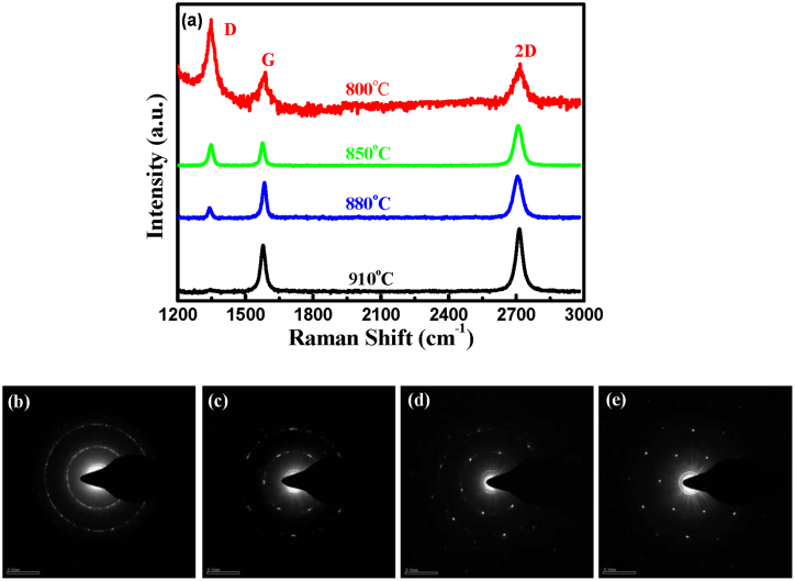
Figure 1(a) shows the Raman spectra acquired from the graphene films deposited at different temperatures. At 800°C or lower, the typical features of graphene, i.e., the 2D peak at ~2710 cm−1 and the G peak at ~1580 cm−1, appear. However, a large defect related D peak emerges near 1350 cm−1 with a peak intensity ratio of ID/IG ≈ 1.8, indicating the presence of defects in the graphene layer. The crystalline quality is gradually improved with increasing temperature from 800°C to 910°C as evidenced by the attenuation in the D peak. The peak intensity ratios ID/IG decrease obviously from 1.8 to 0.04 and no appreciable D peak is observed when the growth temperature is increased to 910°C. The improved crystalline quality is confirmed by selected area electron diffraction (SAED). The sample deposited at 800°C shows SAED pattern in Figure 1(b) with a diffuse diffraction ring pattern typical of a disordered structure. With increasing growth temperature, the SAED pattern of the graphene film changes from a ring pattern to a spot pattern, as shown in Figure 1(c–e) and the optimal temperature determined experimentally is 910°C.
Figure 1. Structural and crystalline quality characterization of graphene films grown at various temperatures.
(a) Raman spectra of graphene films deposited on Ge under the optimal conditions at different temperatures. (b–e) SAED patterns of graphene films deposited directly onto Ge at 800°C, 850°C, 880°C, and 910°C.
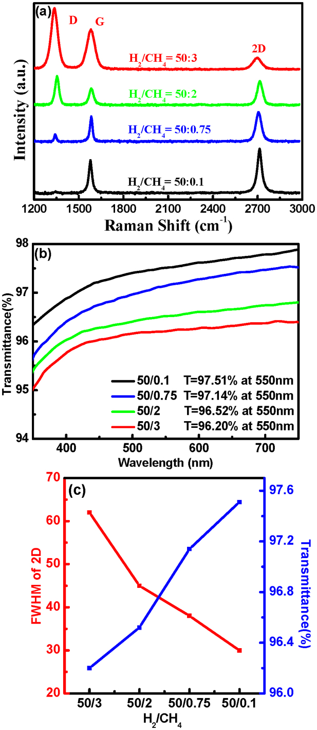
Figure 2(a) depicts the Raman spectra of the graphene films deposited on Ge by varying the H2 to CH4 gas ratios. The temperature is set at the optimized one of 910°C and the time is 100 min to ensure complete coverage of graphene. As the ratio is changed from 50:0.1 (sccm) to 50:3 (sccm), the defect related D peak emerges and the peak intensity increases rapidly. Furthermore, the FWHM of the 2D peak increases gradually from 30 cm−1 to 65 cm−1 (as shown in Figure 2(c)) and the 2D to G peak ratio changes from 1.3 to 0.3. Considering that many factors can affect the Raman spectra of graphene16, it appears that the graphene films grow from one to several layers. To determine the thickness, the transmittance at 550 nm is obtained from the graphene films transferred onto glass slides and the results are presented in Figure 2(b). The optical transmittance diminishes gradually as the H2/CH4 flow ratio is varied from 50:0.1 to 50:3, supplying evidence that the graphene films become thicker. At a flow rate ratio of 50:0.1, a high transparency of 97.51% is observed. Considering an absorbance of ~2.3% for an individual graphene layer24, the graphene film can be inferred to have only one layer. When the H2:CH4 ratio is changed to 50:3, the transmittance drops to 96.20% and the graphene film is composed of several layers. The number of graphene layers is determined by the amount of hydrocarbon gas and in addition, the amount of hydrogen is critical to the graphene layer number since hydrogen balances the production of reactive hydrocarbon radicals and etching of graphite during CVD. If the H2/CH4 ratio is 50:3, etching becomes much slower than the formation of graphene leading to the formation of multi-layered graphene. The optimal H2/CH4 ratio to produce monolayered graphene determined experimentally is 50:0.1.
Figure 2. Structural and optical characterization of graphene films grown at different H2:CH4 ratios.
(a) Raman spectra of graphene films deposited on Ge under the optimal conditions using different H2:CH4 flow ratios. (b) Optical transmittance spectra of the transferred graphene films deposited using different H2:CH4 ratios. (c) FWHM of the 2D peak and transmittance as a function of H2:CH4 ratios.
The growth of homogeneous monolayered graphene and its characterization
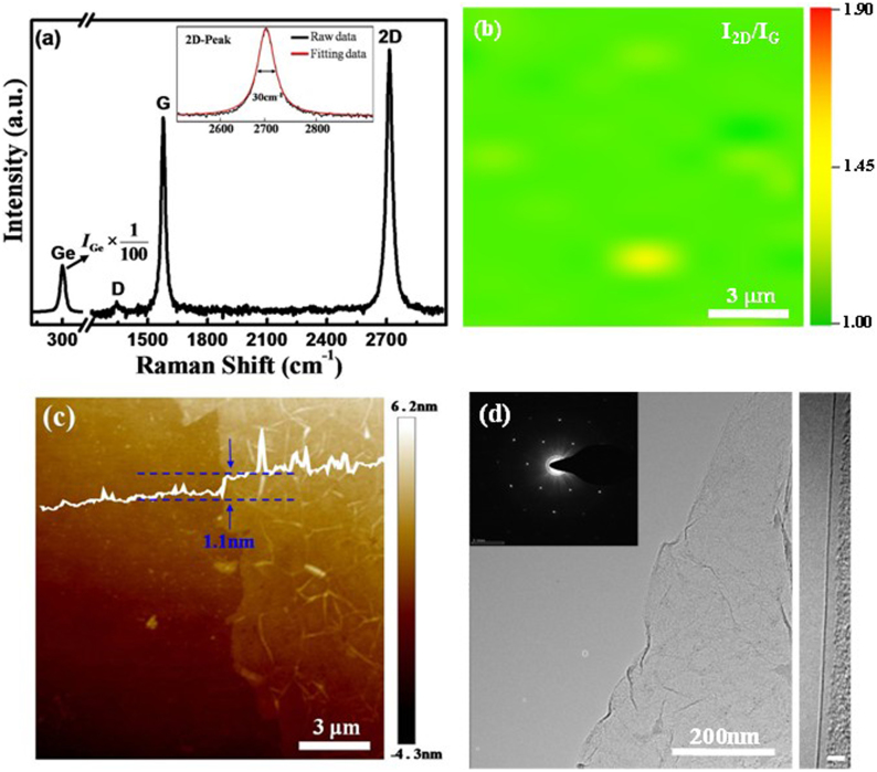
Using the optimal conditions for the growth of monolayered graphene as described above, graphene was deposited on Ge substrates at 910°C with a H2 to CH4 flow rate ratio of 50:0.1 (sccm) for 100 min in an ambient-pressure CVD system. Figure 3(a) depicts the representative Raman spectrum of the as-deposited graphene. The defect-related D peak is strongly suppressed, implying that the graphene film has high quality comparable to that of exfoliated graphene25. Furthermore, as shown in the inset of Figure 3(a), the symmetric 2D peak with a FWHM of ~30 cm−1 can be well fitted by a single Lorentzian curve providing evidence of monolayered graphene26. To determine the quality, uniformity, and thickness of the graphene films deposited on a large-scale on Ge, Raman mapping of the 2D to G peak intensity ratio over a 15 μm × 15 μm area with a spot size of 1 μm and a step size of 1 μm is performed, as shown in Figure 3(b). The I2D/IG ratio is quite uniform over the region investigated and the I2D/IG is in the range of 1–1.5, indicating complete monolayer graphene coverage in the scanned area27. The excellent uniformity is also exhibited across large area as 1 cm × 1 cm (Supplementary Figure S2). Figure 3(c) shows the representative atomic force microscopy (AFM) image of the graphene film transferred from Ge onto 300 nm SiO2/Si. A uniform height of 1.1 nm also suggests that the graphene film is monolayered28. The monolayer feature and high crystallinity of the graphene are also confirmed by transmission electron microscopy (TEM) and SAED, as shown in Figure 3(d). The suspended graphene films on the TEM grids are continuous over a large area and the high-resolution TEM image randomly taken from numerous graphene film edges reveals that the as-grown graphene is monolayered. The SAED pattern of the graphene films is displayed in the inset of Figure 3(d). Only one set of hexagonal diffraction pattern is observed and a single crystalline lattice structure can be inferred.
Figure 3. Large-scale uniform growth of monolayered graphene films on Ge substrate.
(a) Raman spectrum of graphene on Ge substrate. The insert shows the FWHM and the Lorentzian fitting of 2D peak. (b) Two-dimensional Raman mapping of the I2D/IG peak intensity ratio obtained from the graphene deposited on Ge (15 μm × 15 μm region with the step size of 1 μm). (c) Contact -mode AFM image of a graphene film transferred on SiO2 showing the monolayered feature and wrinkles. (d) TEM image and SAED pattern revealing the high crystalline quality of the graphene and HR-TEM image showing that the graphene is monolayered. The scale bar in the HR-TEM image is 3 nm.
Discussion
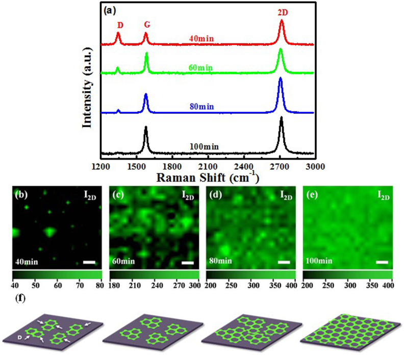
To elucidate the mechanism, graphene films were deposited on Ge for different periods of time under the optimal conditions. As shown in Figure 4(a), as the deposition time is increased, the defect-related D peak disappears gradually and no appreciable D peak is observed when the time is 100 min. However, the Raman spectra obtained from the graphene samples deposited for 120 min or longer are similar to that acquired from the sample deposited for 100 min (not shown here), implying that the growth process of graphene on Ge is self-limited. The attenuation in the D peak is believed to be attributed to the decrease in the domain edges in expanded graphene domains. Expansion of graphene domains is vividly exhibited by the color-coded intensity mapping of the 2D peak over an 15 × 15 μm2 area with a spot size of 1 μm and step size of 1 μm, as shown in Figures 4(b–e). The green regions correspond to graphene patches and the dark regions represent the bare Ge surface. In the initial stage of graphene deposition, the size of the graphene patch is relatively small, and so there is a large number of edge defects relative to the domain of graphene, thereby leading to the remarkable D peak in the Raman spectra. When the deposition time is increased from 40 min to 100 min, the graphene patches grow in two-dimension islands due to excess carbon atoms and finally merge together to form a continuous film, as illustrated in Figure 4(f). Therefore, the contribution from the edge of the graphene domain can be neglected and the corresponding D peak is scarcely observed.
Figure 4. Characterization of graphene grown on Ge substrates for different durations and illustration of graphene growth evolution.
(a) Raman spectra of graphene films deposited on Ge under optimal conditions for different time. (b–e) Color-coded Raman mapping of the 2D peak intensity images of graphene as a function of deposition time. The green features are graphene domains and the dark regions represent the bare Ge surface. The scale bar is 2 μm. (f) Schematic illustration of evolution of the graphene films on Ge for different deposition time.
Nickel and copper are two representative transition metals which have been observed to produce relatively large-scale graphene films by CVD. Graphene films deposited on Ni possess small grain sizes and uncontrollable layer numbers29, but on the other hand, high-quality monolayered graphene films have been produced on Cu16. Therefore, the two mechanisms should be different. It has been proposed that CVD of graphene on Ni, which has high carbon solubility (>0.1 at.%), proceeds via surface segregation followed by precipitation. In addition, a fast cooling rate is required to suppress the growth of multiple-layered graphene30. Owing to the ultralow solubility of carbon in Cu (<0.001 at.%), fabrication of graphene on Cu should not involve C precipitation, but is rather attributed to surface adsorption. According to equilibrium phase diagram of the Ge-C system31, the constituents in the Ge-C alloy are immiscible under equilibrium in the bulk (Supplementary Figure S3). This is similar as the Cu-C system which is known to be mutually immiscible in both the solid and liquid states32. Moreover, unlike the case involving Ni, the properties of the graphene films produced on Ge are the same regardless of whether a fast-cooling process or slow-cooling process is adopted (Supplementary Figure S4). Hence, on account of the negligible carbon solubility in bulk Ge (<0.1 at.%), it is suggested that it is also a self-limiting and surface-mediated process similar to Cu-catalyzed growth of graphene.
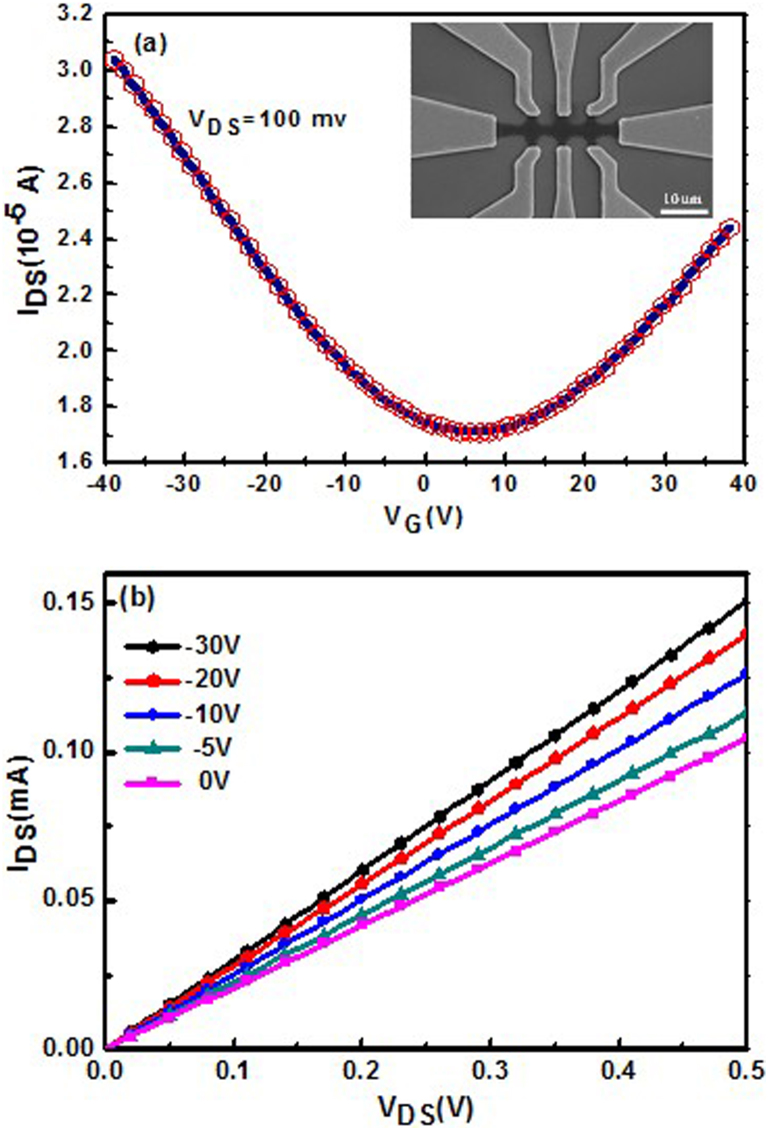
To determine the transport properties of the synthesized graphene films, back-gated graphene field effect transistors (GFETs) were fabricated on 300 nm SiO2/Si substrates15, as shown in the inset of Figure 5(a). Figure 5(a) also shows the highly reproducible transfer characteristics (IDS-VG) of the GFETs measured at room temperature under ambient conditions. The typical IDS-VG curve measured at a VDS of 100 mV shows that the gate can cause either hole or electron conduction. The V-shaped ambipolar transfer characteristic is typical of monolayered graphene with a zero bandgap28. The Dirac point of the GFETs shifts slightly to a positive gate at VG ~ 5 V, demonstrating light p-type hole doping performance. According to the two slopes of the linear regions on both sides of the V-shaped curve, the hole mobility is μh ~ 900 cm2V−1s−1 and the electron mobility is μe ~ 800 cm2V−1s−1, both of which are comparable to values reported recently from transferred CVD graphene19. The presence of defects, wrinkles, and overlaps generated from the transfer process may degrade the performance of GFETs (Supplementary Figure S5(a) and (b)) thus underestimating the carrier mobility of the synthesized graphene film. In the output characteristics of the GFETs (Figure 5(c)), the linear IDS-VDS behavior indicates a good ohmic contact between the Ti/Au contact and graphene channels. In addition, IDS increases with deceasing VG from 0 to −30 V and it is indicative of p-type behavior as well. The electrical transport data also reveal that the graphene deposited on Ge is of good quality which can be further improved by refining the deposition process.
Figure 5. Electrical properties of graphene transferred from Ge to SiO2/Si substrate.
(a) IDS-VG curves of graphene transistors at VDS = 100 mV. The insert shows the SEM image of a back-gated GFET. (b) IDS-VDS curves of graphene transistors at different VG.
In this work, we have developed a facile synthesis method for large-scale and high-quality graphene directly on Ge substrates by APCVD which conclusively certifies that semi-metal Ge has very effective catalytic ability for direct fabrication of graphene. Parametric studies show that the superior quality and homogeneous monolayer graphene in large scale can been achieved on Ge substrates directly with the optimal growth conditions. On the basis of these results, we propose a self-limiting mechanism for graphene growth on Ge substrate, which is an analogue of graphene on Cu foil due to extremly low carbon solubility. The obtained GOG substrate is scalable and compatible with the mainstream microelectronics technology, thus paving the way to the application of graphene in microelectronic field.
Methods
CVD growth of graphene
The graphene films were grown on Ge substrate by an APCVD method. Graphene sample was prepared with H2:CH4 = 50:0.1 sccm at the growth temperature of 910°C for 100 min. After growth, the methane (CH4) gas and the furnace were turned off, and the furnace was cooled down to room temperature under the same flow rates of H2 and Ar at the growth stage. Further experimental details are described in the Supplementary Information.
Transferring the graphene films to the target substrates
After the APCVD process, graphene film was transferred by a PMMA-assisted wet-transfer method. The graphene/PMMA film was transferred into water by etching the Ge substrate. After the removal of the PMMA film in acetone, the film can be transferred to any substrate for analysis and characterization subsequently. Further experimental details are described in the Supplementary Information.
Characterization
Raman spectra (HORIBA Jobin Yvon HR800) were obtained using a Ar+ laser with a wavelength of 514 nm and a spot size of 1 μm. The spectra were recorded with a 600 lines/mm grating. Transmission electron microscopy (TEM, FET-Tecnai G2F20 S-7WIN) is utilized to ascertain crystallographic information and also to determine the number of graphene layers. Electrical measurements were performed in ambient condition using Agilent (B1500A) semiconductor parameter analyzer. On quartz slides, optical transmittance spectra were collected in a UV solution u-4100 spectrophotometer. Transmittance properties were measured using a wavelength of 550 nm. The AFM images of graphene transferred onto the 300 nm SiO2/Si were taken with a Bruker(Icon). The scanning electron microscopy image of GFETs was taken with HITAGHT S-3400N microscope.
Author Contributions
Z.D. and X.W. Supervised the project. M.Z., S.L. and Z.D. conceived the experiment. G.W., Y.Z., G.D. and D.J. performed the experiments. X.X. contributed to the discussion. Q.G. and G.W. analyzed the data and prepared the figures. Z.D. and P.C. wrote the nanuscript.
Supplementary Material
supporting materials
Acknowledgments
We thank the supports from the National Natural Science Foundation of China under Grant No. 61176001, 51222211, 61006088, National Basic Research Program of China (973 Program) under Grant No. 2010CB832906, Pujiang Talent Project of Shanghai under Grant No. 11PJ1411700, One Hundred Talent project from Chinese Academy of Sciences, Hong Kong Research Grants Committee (RGC) General Research Funds Nos. CityU 112510 and 112212, as well as City University of Hong Kong Applied Research Grant (ARG) No. 9667066.
References
- Geim A. K. & Novoselov K. S. The rise of graphene. Nat. Mater. 6, 183–191 (2007). [DOI] [PubMed] [Google Scholar]
- Bunch J. S. et al. Electromechanical resonators from graphene sheets. Science 315, 490–493 (2007). [DOI] [PubMed] [Google Scholar]
- Garcia-Sanchez D. et al. Imaging mechanical vibrations in suspended graphene sheets. Nano Lett. 8, 1399–1403 (2008). [DOI] [PubMed] [Google Scholar]
- Schedin F. et al. Detection of individual gas molecules adsorbed on graphene. Nat. Mater. 6, 652–655 (2007). [DOI] [PubMed] [Google Scholar]
- Wehling T. O. et al. Molecular doping of graphene. Nano Lett. 8, 173–177 (2008). [DOI] [PubMed] [Google Scholar]
- Bae S. et al. Roll-to-roll production of 30-inch graphene films for transparent electrodes. Nat. Nanotechnol. 5, 574–578 (2010). [DOI] [PubMed] [Google Scholar]
- Wu W. et al. Wafer-scale synthesis of graphene by chemical vapor deposition and its application in gas sensing. Sensors and Actuators B. 150, 296–300 (2010). [Google Scholar]
- Lemme M. C. et al. A graphene field-effect device. IEEE Electron Device Lett. 28, 282–284 (2007). [Google Scholar]
- Mohanty N. et al. Graphene-based single-bacterium resolution biodevice and DNA-transistor-interfacing graphene-derivatives with nano and micro scale biocomponents. Nano Lett. 8, 4469–4476 (2008). [DOI] [PubMed] [Google Scholar]
- Lin Y. -M. et al. 100 GHz graphene transistor from wafer-scale epitaxial graphene. Science 327, 662–662 (2010). [DOI] [PubMed] [Google Scholar]
- Wang X. et al. Transparent carbon films as electrodes in organic solar cells. Angew. Chem. Int. Ed. 47, 2990–2292 (2008). [DOI] [PubMed] [Google Scholar]
- Ohno Y. et al. Electrolyte-gated graphene field-effect transistors for detecting pH and protein adsorption. Nano Lett. 9, 3318–3322 (2009). [DOI] [PubMed] [Google Scholar]
- Novoselov K. S. et al. Electric field effect in atomically thin carbon films. Science 306, 666–669 (2004). [DOI] [PubMed] [Google Scholar]
- Berger C. et al. Electronic confinement and coherence in patterned epitaxial graphene. Science 312, 1191–1196 (2006). [DOI] [PubMed] [Google Scholar]
- Park S. et al. Chemical methods for the production of graphenes. Nat. Nanotechnol. 4, 217–224 (2009). [DOI] [PubMed] [Google Scholar]
- Li X. et al. Large-area synthesis of high-quality and uniform graphene films on copper foils. Science 324, 1312–1314 (2009). [DOI] [PubMed] [Google Scholar]
- Liu M. et al. Thinning segregated graphene layers on high carbon solubility substrates of rhodium foils by tuning the quenching process. ACS Nano. 6, 10581–10589 (2012). [DOI] [PubMed] [Google Scholar]
- Yu Q. et al. Graphene segregated on Ni surfaces and transferred to insulators. Appl. Phys. Lett. 93, 113103 (2008). [Google Scholar]
- Yang H. et al. Graphene Barristor, a Triode Device with a Gate-Controlled Schottky Barrier. Science 336,1140–1143 (2012). [DOI] [PubMed] [Google Scholar]
- Chen J. et al. Oxygen-aided synthesis of polycrystalline graphene on silicon dioxide substrates. J. Am. Chem. Soc. 133, 17548–17551 (2011). [DOI] [PubMed] [Google Scholar]
- Tang S. et al. Nucleation and growth of single crystal graphene on hexagonal boron nitride. Carbon 50, 329–331 (2012). [Google Scholar]
- Novoselov K. S. et al. A roadmap for graphene. Nature 490, 192–200 (2012). [DOI] [PubMed] [Google Scholar]
- Chau R. et al. Integrated nanoelectronics for the future. Nat. Mater. 6, 810–812 (2007). [DOI] [PubMed] [Google Scholar]
- Nair R. R. et al. Fine structure constant defines visual transparency of graphene. Science 320, 1308–1308 (2008). [DOI] [PubMed] [Google Scholar]
- Ferrari A. C. et al. Raman spectrum of graphene and graphene layers. Phys. Rev. Lett. 97, 187401 (2006). [DOI] [PubMed] [Google Scholar]
- Park J. et al. Epitaxial graphene growth by carbon molecular beam epitaxy (CMBE). Adv. Mater. 22, 4140–4145 (2010). [DOI] [PubMed] [Google Scholar]
- Peng Z. et al. Direct growth of bilayer graphene on SiO2 substrates by carbon diffusion through nickel. ACS Nano. 5, 8241–8247 (2011). [DOI] [PubMed] [Google Scholar]
- Dai B. et al. Rational design of a binary metal alloy for chemical vapour deposition growth of uniform single-layer graphene. Nat. Commun. 2, 522–528 (2011). [DOI] [PubMed] [Google Scholar]
- Reina A. et al. Large area, few-layer graphene films on arbitrary substrates by chemical vapor deposition. Nano Lett. 9, 30–35 (2009). [DOI] [PubMed] [Google Scholar]
- Kim K. S. et al. Large-scale pattern growth of graphene films for stretchable transparent electrodes. Nature 457, 706–710 (2009). [DOI] [PubMed] [Google Scholar]
- Olesinski R. W. et al. Binary alloy phase diagrams., 2nd Ed., Ed.Massalski, T. B. 1, 849 (1990).
- Chu J. P. et al. Microstructure and properties of Cu-C pseudoalloy films prepared by sputter deposition. Metal. Mater. Trans. A. 29A, 647–658 (1998). [Google Scholar]
Associated Data
This section collects any data citations, data availability statements, or supplementary materials included in this article.
Supplementary Materials
supporting materials


