Abstract
We describe the design, characterization, and demonstration of a fully integrated single-photon avalanche diode (SPAD) imager for use in time-resolved fluorescence imaging. The imager consists of a 64-by-64 array of active SPAD pixels and an on-chip time-to-digital converter (TDC) based on a delay-locked loop (DLL) and calibrated interpolators. The imager can perform both standard time-correlated single-photon counting (TCSPC) and an alternative gated-window detection useful for avoiding pulse pile-up when measuring bright signal levels. To illustrate the use of the imager, we present measurements of the decay lifetimes of fluorescent dyes of several types with a timing resolution of 350 ps.
I. Introduction
Fluorescent dyes have long been used as markers to allow visualization of biological processes and analytes. Applications include imaging of blood flow [1], neuronal activity [2], and drug delivery and uptake [3]. Emerging techniques such as confocal [4] and multi-photon [5] microscopy allow three-dimensional imaging of living tissue. Fluorescent dyes are also used extensively as labels for proteins and DNA in immunoassays and microarray applications [6].
Traditionally, fluorescence microscopy has been performed using spectrally-discriminated intensity measurement, with thin-film filters and dichroic mirrors used to isolate the dye emission from the excitation light source [7]. This filtering is complicated by the fact that for many dyes the spectral distance, known as the “Stokes shift,” between the excitation and emission peaks is narrow, on the order of 10-30 nm. Additional background light can come from sample or environmental autofluorescence and source bleed-through. Dye emission intensity can also vary with dye concentration, light-path length, and the density of intervening material, and can attenuate over time through photobleaching [8].
Fluorescence lifetime imaging microscopy (FLIM), the technique of measuring the rate of decay of a fluorophore instead of its intensity, is largely immune to these challenges. The lifetime of a dye (generally denoted by τ) is the time from an impulse excitation until the emission intensity has decayed to 1/e of its peak. For fluorophores, such as many organic dyes, whose decay profiles are mono-exponential, i.e., I(t) = I0e–t/τ, the lifetime corresponds to the average time until the emission of the first photon after excitation. Many commonly used fluorophores, notably semiconductor quantum dots, have decays that more closely resemble multi-exponential functions, . In this case, multiple, average, or dominant lifetimes can be considered [7].
Lifetime is an intrinsic property of the fluorophore, dependent on its chemical composition and conformation. However, through excited-state reactions, it can be affected by the dye's chemical and physical environment. This has been exploited in the use of dyes with lifetimes sensitive to voltage, calcium and other ion concentrations, pH, and the proximity of secondary dyes through a process known as fluorescence resonance energy transfer (FRET) [8]-[12].
The most common sensor used in FLIM systems is the photomultiplier tube (PMT), a high-gain instrument that converts a single photon into an electrical pulse. In the usual time-correlated single-photon counting (TCSPC) setup, the PMT output is connected to a time-to-digital converter (TDC) which records the time of arrival of the first photon emitted after stimulation of the fluorophore by a pulsed light source. By repeating this measurement, a histogram of arrival times can be constructed from which the fluorescence lifetime(s) can be deduced [7]. While PMTs have excellent sensitivity and PMT FLIM systems can have timing resolution limited only by jitter and the resolution of the TDC, PMTs are bulky, expensive instruments and multipixel images require scanning the excitation source across the sample, leading to increased complexity and reduced frame-rate. Furthermore, PMTs cannot be electrically gated, so optical filtering is still required to prevent the source from saturating the detector [13].
Alternatively, CMOS and CCD imagers (often with the use of a gated intensifier) have been used for FLIM measurements by gating them for fixed intervals following excitation [14]. By comparing the integrated fluorescence intensity during intervals with advancing offsets, the fluorescence lifetime can be calculated. While these sensors are easily integrated into multipixel arrays, they have low or unity gain, forcing long integration times and limiting image acquisition rates. In addition, the number of exponential components that can be identified by these systems is limited by the number of window offsets used [15].
Single-photon avalanche diodes (SPADs) are qualitatively PMT-like detectors. The ability to integrate them in CMOS has provided a new platform for FLIM imaging that combines the benefits of PMTs and integrated imagers. SPADs have high quantum efficiency and very low intrinsic jitter. We have developed and characterized a 64-by-64 pixel FLIM imager in a 0.35-μm standard CMOS process [16]. The imager has active SPAD pixels and on-chip time-to-digital conversion, designed for 50-ps timing resolution. We have demonstrated the use of the imager for quantification of fluorescence lifetimes.
This paper is organized as follows. Section II introduces fluorescence lifetime imaging techniques. Section III describes the prototype imager. Section IV contains the characterization of the imager as well as fluorescence lifetime measurement results. A statistical analysis of gated-window mode detection is provided in the Appendix.
II. Time-Resolved Fluorescence Imaging
Time-resolved imaging differs from standard imaging in that the intensity of the signal is not directly measured. Instead, the arrival times of photons are collected, measured relative to the time of an excitation impulse, usually generated by a pulsed laser source. A timing diagram for time-correlated single-photon counting (TCSPC) is shown in Fig. 1. At time tri, the light source is triggered, exciting the dye. When the detector senses a photon emitted by the dye, the difference between the time of arrival, ari, and tri is recorded. In practice, all time-to-digital converters (TDCs) have finite timing resolution and time values are quantized in bins. The measurement is repeated and a histogram of hits-per-time-bin is constructed from which the intensity decay profile is deduced.
Fig. 1.

Timing diagram for TCSPC measurement
The histogram will precisely correspond to the dye intensity decay only if a single fluorophore is stimulated. As the signal intensity increases, the histogram is skewed towards earlier time bins, a well-known phenomenon called pulse pile-up [18]. In some cases, this nonlinearity can be corrected mathematically [19] or algorithmically [20]. Usually, however, it is mitigated by maintaining a low signal level, for example by allowing fewer than one photon to be detected per one hundred measurements [18].
The ability to electrically or optically gate the detector allows an alternative measurement technique, gated-window (GW) detection, that mitigates pile-up nonlinearities. A timing diagram for this approach appears in Fig. 2. During each measurement, the detector is enabled for a window wi = [ti, ti+tw], of fixed duration, tw, and offset, ti, after stimulation of the dye. The light source is pulsed and a binary output, determined by whether or not a photon is detected during the window, is recorded. A number of measurements, Mi, is taken for each of several window positions as ti is varied and the number of successful detections, H(wi), for each window position is collected. The intensity of the signal is approximated as Ĥ(ti) = H(wi)/Mi, the fraction of measurements taken in each window resulting in hits. The timing resolution of the system is Δt, the difference between successive ti. As prior studies of gated-window measurement [21], [22], [13] have focused on integrating or multiple-photons-per-window detection, a brief analysis of the technique in the present context is provided in the Appendix.
Fig. 2.
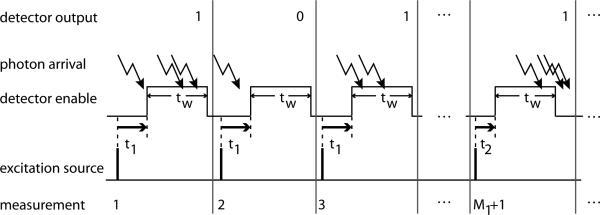
Timing diagram for GW measurement
Timing resolution and measurement window size are important characteristics of time-resolved fluorescence measurement systems. Finer timing resolution reduces quantization noise, and allows measurement of shorter lifetime components and better discrimination between components of multiexponential decays with a reduced measurement count. Based on statistics derived in [17], a timing accuracy of at least one tenth of the shortest measured lifetime component should be used. Long measurement windows, on the other hand, facilitate measurement of long lifetime components. The effect of these parameters on measurement variance is treated in [17]. In addition to process timing limitations, area and I/O bandwidth place constraints on the measurement window width and timing resolution. Given these considerations in combination with the the typical lifetime range of 1-30 ns of many standard dyes including quantum dots, a least significant bit (LSB) of 50 ps and measurement resolution of ten bits, giving a window length of 51.2 ns, were chosen as the design targets for the TDC in this work.
III. Imager Description
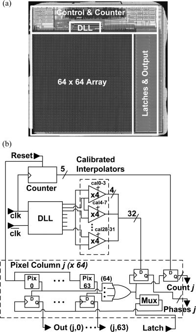
A die photograph and system-level diagram of the imager prototype are shown in Fig. 3. The imager consists of a 64-by-64 array of SPAD pixels, on-chip time-to-digital conversion, and supporting circuitry. It is fabricated on a 4-mm-by-4-mm die in a 0.35-μm high-voltage CMOS process and supports both the TCSPC and GW modes described in Section II. The active area of each pixel is 15 μm2 with a pixel pitch of 40 μm.
Fig. 3.
Die photograph (a) and system overview (b) of the prototype imager chip
As shown in Fig. 3, the primary subsystems of the imager are the timing generation circuitry, consisting of a counter, a delay-locked loop (DLL), and a set of calibrated interpolators, the array of sensor pixels, and a set of latches at the output of each pixel column. The latches store the timing information (Count j and Phases j) as well as the output state of each pixel in the column (Out (j,i)), determined by whether a photon was detected at that pixel during the measurement. They are triggered by a photon arrival event to any pixel in the column, or by an external signal (Latch) for use in GW mode. The Reset signal allows synchronization of the timing and pixel circuits. Details are given below.
A. Technology Considerations
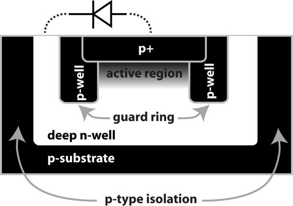
The single-photon avalanche diode sensors are p+/deep-n-well diodes reverse-biased above their breakdown voltage. A photon entering the depletion region of the diode can generate an electron-hole pair and, through subsequent impact ionization, lead almost immediately to avalanche breakdown and a concomitant reverse current spike. The higher the excess voltage above breakdown, the more readily an avalanche is produced and the more sensitive the detector. The maximum practical excess voltage is limited by the dark count rate (DCR) which also increases with increasing excess voltage. Dark counts, which are avalanche events in the absence of light, result from carriers thermally generated from traps acting as generation centers [23].
Two considerations allow for the successful fabrication of SPADs in a standard CMOS process. Firstly, the technology must allow for a low defect density, making technologies that use LOCal Oxidation of Silicon (LOCOS) for field oxide growth preferable to those that employ Shallow Trench Isolation (STI) due to the higher quality of Si/SiO2 interface with thermally grown LOCOS oxide. Secondly, implants must be available to allow the inclusion of a p-type guard ring around the sensor junction, as shown in Fig. 4. Without this guard ring, the breakdown voltage is reduced by the increased electric field near the border of the junction, preventing the formation of a suitable active region [24]. Despite attempts to fabricate SPADs in more advanced technologies, which invariably utilize STI, at this time the high-voltage 0.35-μm technology used here remains the most aggressive standard technology in which CMOS SPADs with dark count rates lower than 100 kHz have been successfully fabricated and demonstrated [25], [26], [27]. The extra implants in the high voltage process enable the fabrication of the guard ring. The target timing resolution of 50 ps is well below the technology slow-corner fan-out-of-four (FO4) delay of 184 ps, requiring the use of interpolated clock phases for the design of the TDC as described below.
Fig. 4.
CMOS SPAD as fabricated in a high-voltage 0.35-μm CMOS process
B. Pixel Architecture
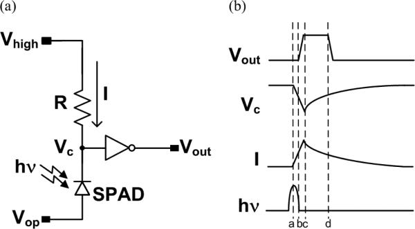
The schematic of a standard passive SPAD pixel and waveforms showing a photon-capture event are shown in Fig. 5. The SPAD is reverse-biased between the cathode voltage, Vc, and Vop, with Vc – Vop > Vbd, the diode breakdown voltage. Initially the current is zero and Vc = Vhigh. When a photon triggers an avalanche in the SPAD (time a in Fig. 5b), the avalanche current, I, is forced through the resistor, R, the cathode is pulled down below the threshold voltage of the inverter, and an output pulse is registered on Vout (time b). When Vc is low enough such that the diode is no longer reverse-biased above its breakdown voltage, the avalanche is quenched (time c). The diode then recharges toward Vhigh, with a time constant determined by R and the capacitance at the cathode, dominated by the junction capacitance of the diode, C (approximately 45 fF in our case). At the end of the cycle (time d), Vout is reset and the pixel is re-enabled.
Fig. 5.
Passive SPAD pixel circuit (a) and waveforms showing a capture event for a photon (b)
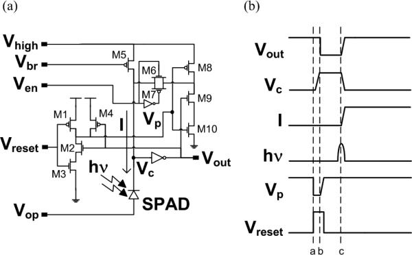
Active pixel circuits decrease the recharge time over passive designs and allow gating of the SPAD [28]. Our pixel circuit, which incorporates an active reset, and the associated photon-capture waveforms are shown in Fig. 6. The basic passive pixel circuit of Fig. 5a is present as the subcircuit consisting of the SPAD, M5, and the output inverter. The purpose of the transmission gate M6/M7, controlled by Ven, is to interrupt the feedback path associated with the active reset and allow operation in passive mode. Vbr, which biases the cathode pseudoresistor, is typically tied to ground. Vhigh and Vop determine the diode bias. Values need to be chosen such that Vout is low when the diode is reset, and high when it is quenched, i.e., when Vc – Vop = Vbd. A rising edge to Vreset turns M8 on, providing a low-impedance path to quickly recharge the diode (time a in Fig. 6b). This active path reduces the reset time by almost three orders of magnitude over that of the passive circuit (from approximately 37 ns to approximately 60 ps). Once the diode is recharged, the output inverter flips (time b), turning off M8 through the action of M4 and M2. The pixel is then fully reset and ready to sense a photon. The pixel responds to a photon arrival event (time c) much in the same way as the passive circuit. Here, however, the half-latch M9 prevents Vc from recharging until the arrival of the next Vreset pulse (M10 is on). In this way, the state of the output is preserved for later readout.
Fig. 6.
Active SPAD pixel circuit (a) and waveforms showing a capture event for a photon (b)
C. Time-to-Digital Conversion
Several architectures have been proposed for sub-gate-delay time-to-digital conversion circuitry, including the time-stretching technique [29] and techniques based on Vernier delay lines [30]. These, however, are not well-suited to this application. The maximum conversion rate of a time-stretching converter is limited by the speed of the technology and is proportional to the resolution of the converter. Vernier techniques, on the other hand, require an individual delay line for each TDC instance, with a significant area cost and inevitable variation due to mismatch. The design chosen for this system does not suffer from these limitations and is appropriate for a multiple-TDC system. A single accurate timing-signal generator is routed to sets of latches clocked by timing events. Additional TDCs require only the limited area associated with additional latch sets. As digital calibration is used extensively for offset and duty-cycle correction, matching is of minimal concern. Furthermore, the multiphase clock is stabilized by a supply-regulated DLL which is relatively insensitive to process, voltage, and temperature (PVT) variations. The design is similar to one recently described in [31]. A major difference, however, is our use of digital interpolation, facilitating mismatch correction, instead of a passive delay chain, to achieve fine timing resolution.
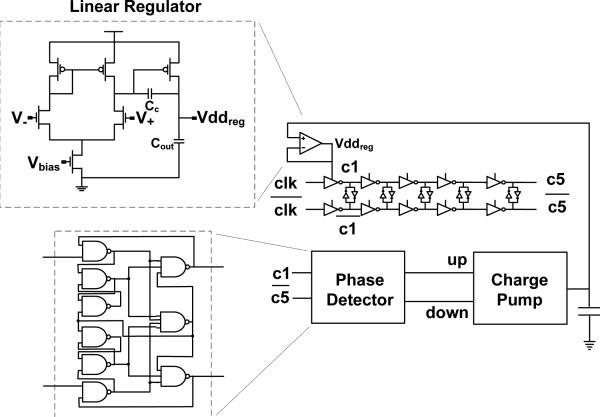
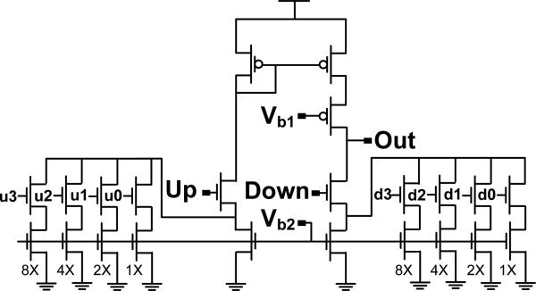
The structure of the TDC can be seen in Fig. 3b. The timing-signal generator, shared by all pixels, consists of a five-bit digital counter (coarse timing) and a thirty-two-phase clock generator (fine timing). The sixty-four sets of latches to register event times are shared by each column. A low-swing differential sinusoidal input clock is converted through a pair of self-biased amplifiers [32] to a complementary full-rail clock waveform, one phase of which drives the counter. The clock also feeds a DLL-stabilized delay line consisting of four differential delay elements, as shown in Fig. 7, synchronized such that four delay times correspond to one half of a clock period. Each delay element is a supply-regulated inverter pair with weakly cross-coupled outputs. The coupling inverters also use the regulated supply, to improve PVT tracking and avoid source-drain inversion. The DLL feedback control, based on a design in [33], consists of a phase comparator and charge pump to a linear regulator which controls the supply voltage of the delay elements. The signals labeled c1 and c̄5 in Fig. 7 are passed through level shifters to bring them to full-rail and fed to the phase detector, a simple NAND-based design in which the difference in the average values of the up and down output signals corresponds to the lead or lag of the two inputs. The charge pump, shown in Fig. 8, is digitally calibrated with binary-weighted current sources to correct for mismatches in up and down strength. The bias voltages, Vb1 and Vb2 control the magnitude of the current sent to the integrating capacitor, affecting the locking time and offset.
Fig. 7.
Delay-locked loop design
Fig. 8.
Calibrated charge pump
The linear regulator is shown in the upper inset of Figure 7. A 1 pF polysilicon-polysilicon capacitor (Cc) is used for compensation, assuring stability by increasing the phase margin from 13° to 77° with an expected current load of 8.3 mA. With this load, the open-loop gain and bandwidth of the regulator are 54 dB and 245 kHz, respectively. A 4.85 pF MOS capacitor (Cout) is used to stabilize the output. In simulation, supply voltage variations are attenuated more than 35 dB from DC to over 1 MHz. Also in simulation, the DLL locks to a 625 MHz input clock in 1.2 μs.
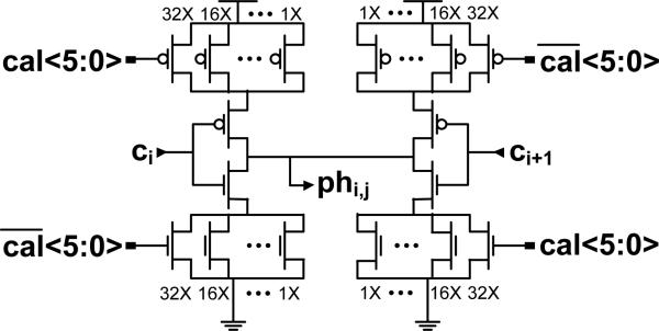
To achieve the full 50-ps timing accuracy, the clock is further divided by feeding pairs of the eight outputs of the delay chain each to four identical six-bit binary-weighted current-starved interpolators (Fig. 9) with a delay range of approximately 25 ps to 440 ps. As the interpolators also use the regulated supply, their outputs are fed to level shifters to raise them to full-rail values. The five counter bits and thirty-two phase bits are passed to sets of D flip-flops in each column. In TCSPC measurements, the flip-flops are latched by the first arriving pixel output signal from the column. In this way, the coarse and fine timing information is stored as a 37-bit word. An additional error bit is generated if the counter overflows before the arrival of the latch signal. The same column latch signal stores the output state of each pixel in another set of D flip-fops. Sixty-four digital output pads allow all the latched bits to be serially read from the chip after each measurement.
Fig. 9.
Calibrated interpolator
D. Modes of Operation
The imager operates in three modes: calibration mode, TCSPC mode, and GW mode.
1) Calibration mode
This mode allows calibration of the charge pump and the interpolators. The pixels are disabled and the counter-reset and timing-latch controls are directly connected to external start and stop inputs, respectively. The digital calibration bits can be chosen such that the time measured by the imager matches an accurate external timing source. The start signal must be synchronous with the system clock for the multiphase clock data to be meaningful. Differences in latched timing data due to mismatched wire loading across the columns are inconsequential as timing histograms for each pixel are independent.
2) TCSPC mode
When the imager receives a trigger signal from off-chip, the counter and all of the pixels are reset. As in calibration mode, the trigger must be synchronous with the system clock. A rising edge on the output of any pixel in a column latches the timing information and the state of the output of each pixel in that column. A time-out signal generated by overflow of the counter ends the measurement. By design, only one result per column per measurement is allowed and if more than one pixel in a column has a positive output, an error bit is set for that column. If the maximum allowed signal level is set to one photon per pixel per one hundred measurements,1 error bits will be generated on average in
| (1) |
of measurements. This small potential cost in throughput is compensated by the reduced area and bandwidth requirements of accepting only one result per column per measurement.
3) GW mode
To allow general flexibility in varying window start and stop times, GW mode does not utilize on-chip timing circuitry. Instead, an accurate off-chip timing generator is used to send start and stop signals as in calibration mode. In this case, however, the start signal resets the pixels, and the stop signal latches the state of the output of each pixel. These signals are routed to each pixel along similar paths to minimize skew between start and stop times.
IV. Measurement Results
In this section we present measured performance characteristics of the SPAD imager as well as the results of time-resolved measurements of fluorescent dyes. The imager characterization is summarized in Table I.
TABLE I.
Prototype performance summary
| Chip | Technology | 0.35-μm high-voltage CMOS |
| Area | 16 mm2 | |
| Resolution | 64-×-64 pixels | |
| Pitch | 40 μm | |
| Supply Voltage | 4.0 V | |
| Current Consumption | 350 mA | |
| TDC | LSB | 350 ps |
| Jitter | <1 LSB | |
| INL | 1.37 LSB | |
| DNL | 1.04 LSB | |
| SPAD | DCR | 1059 Hz |
| Maximum PDP | 4.7% | |
| at Wavelength | 440 nm | |
| Array | GW Measurement Rate | 1144 measurements/s |
| TCSPC Measurement Rate | 718 measurements/s | |
| Maximum Frame-rate | 3.9 Hz | |
A. Measurement Setup
The imager is packaged in a 272-pin BGA package, seated in a socket on a custom printed circuit board (PCB). A machined C-mount adapter permits attachment of the PCB to the standard camera port of a microscope. The light source is a PiLAS gain-switched 406-nm picosecond diode laser with a full duration at half maximum of approximately 40 ps. The output of a Agilent 8257C analog signal generator is fed through a balun to the differential clock input pins of the imager. A Stanford Research Systems DG535 delay generator synchronized to the clock source provides the start and stop signals in calibration mode, and the pixel-reset and laser-trigger signals in the two measurement modes. The entire system is controlled by a Xilinx XC2V1000 FPGA. Data can be stored in two on-board Cypress 36-Mbit SRAM chips or read directly through a parallel port interface to a PC for processing.
B. Timing Characterization
During the design of DLL, the load current that the linear regulator must supply was miscalculated. The regulator was designed for a current load of 8.3 mA. In actuality, the load, which varies directly with clock frequency, is 50 mA at 625 MHz. With this load, the regulator has an excessive closed loop attenuation of 42 dB. To achieve a timing error of less than 10 ps, the attenuation must be limited to 180 mdB. By reducing the clock frequency to 360 MHz, with an associated load current of 31.4 mA, and increasing the supply voltage to 4.0 V from the nominal 3.3 V, the attenuation is reduced below this level. In this case, the open-loop DC gain and bandwidth of the regulator are 58 dB and 255 kHz, respectively. At 360 kHz, however, the lower-than-intended regulated supply voltage makes the slew rate passed to the interpolators too slow for full thirty-two-phase differentiation, though interpolation is still critical for duty-cycle correction. In the end, eight phases are used for a final timing accuracy of 350 ps. All measured results use this configuration with 1 LSB = 350 ps. With a 3.3 V supply, the maximum frequency at which the DLL reliably locks is 250 MHz. The 625 MHz target frequency could be met with a 3.3 V supply if the output transistor of the linear regulator were sized eight times larger. As the 625 MHz clock was successfully brought onto the chip and the behavior of the interpolators has been verified, it is likely that 50 ps timing would be realizable in a corrected implementation.
As coarse and fine timing are orthogonal, their nonlinearities are measured independently. The absolute DNL and INL are bounded by the sums of the maxima of the respective coarse and fine measurements. For the fine timing, linearity depends largely on calibration. The best measured fine DNL and INL are 0.12 and 0.16 LSB, respectively. For the coarse timing, linearity depends on the alignment of the output edges of the counter which, in turn, depends on the clock frequency. The counter is designed to ensure a coarse timing DNL of less than 25 ps at 625 MHz. At 360 MHz, the edges fall slightly out of phase and the measured DNL is 0.92 LSB with a measured INL of 1.21 LSB. From these values, the total DNL is calculated to be 1.04 LSB and the total INL is 1.37 LSB.
C. Sensor Characterization
1) Photon detection probability
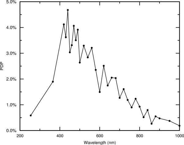
The photon detection probability (PDP) of a typical pixel, defined as the probability of detecting a photon incident on the sensor, is measured using a broad-spectrum light source, a monochromator, and an integrating sphere, together with a calibrated photodetector. The diode bias voltage is approximately 2.7 V above Vbd. A graph of the PDP of the pixel over a range of wavelengths is shown in Fig. 10. The maximum of 4.7% occurs at 440 nm. This wavelength is well into the blue because of the relatively shallow depletion region of the p+/deep-n-well photodiode.2
Fig. 10.
Pixel PDP
2) Noise
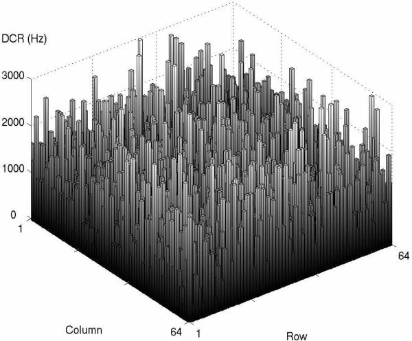
Noise in SPADs is characterized by the dark count rate (DCR), which generally has a high variance due to its dependence on the exact configuration and number of traps in the the diode. DCR measurements were performed with a diode excess bias voltage of 2.7 V. A graph of the DCR across the array is shown in Fig. 11. The average DCR is 1059 Hz or 1502 photons/μm2 · s, with a standard deviation of 547 Hz. The average DCR corresponds to two dark photons per one thousand TCSPC measurements. This noise is uncorrelated and can be averaged out by increasing the number of measurements taken.
Fig. 11.
Array dark count rate
3) Instrument impulse response
For time-resolved measurements, the instrument response function (IRF) of the sensor is convolved with the fluorophore's response to the excitation source. While the ideal IRF is a -function, in practice, SPAD IRFs are characterized by spreading and an exponential tail [34]. This complicates the recovery the original signal from the measurement data and, in general, the more the IRF deviates from the ideal, the more data is needed for averaging. In addition, if the exponential tail of the IRF is longer than the time constant of the fluorescence decay, the effective background signal is augmented by the magnitude of the impulse response, increasing the number of counts needed per measurement.
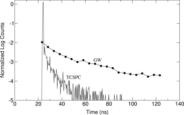
Plots of the IRF of a pixel in TCSPC and GW modes appear in Fig. 12. These measurements are performed with the PiLAS 406-nm laser diode as an impulse source. The tail of the response as measured in GW mode is much greater than that measured in TCSPC mode. The tails are due in part to carriers generated outside of the high-field multiplication region of the diode that diffuse into it, causing delayed triggering of the SPAD [35]. In addition, carriers generated by the flood of photons during the impulse fill deep-level traps in the vicinity of the multiplication region; these carriers are subsequently released by the traps, contributing to the tails, similar to the phenomenon of afterpulsing in passive SPAD systems [36]. It is this second component of the response tail that differs between TCSPC and GW modes. In GW mode, the diode is not yet enabled when the laser is triggered. Carriers that would contribute to the impulse spike in TCSPC mode are instead available to fill traps for later release, creating the long tail in the GW mode impulse response.
Fig. 12.
Log plots of the measured TCSPC and GW instrument response functions
Plots of the instrument response of a pixel in TCSPC and GW modes appear in Fig. 12. These measurements are performed with the PiLAS 406-nm laser diode as an impulse source. The tail of the response as measured in GW mode is much greater than that measured in TCSPC mode. The tails are due in part to carriers generated outside of the high-field multiplication region of the diode that diffuse into it, causing delayed triggering of the SPAD [35]. In addition, carriers generated by the flood of photons during the impulse fill deep-level traps in the vicinity of the multiplication region; these carriers are subsequently released by the traps, contributing to the tails, similar to the phenomenon of afterpulsing in passive SPAD systems [36]. It is this second component of the response tail that differs between TCSPC and GW modes. In GW mode, the diode is not yet enabled when the laser is triggered. Carriers that would contribute to the impulse spike in TCSPC mode are instead available to fill traps for later release, creating the long tail in the GW mode IRF.
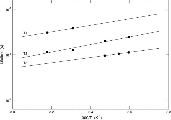
A trap-based explanation for the difference between the GW and TCSPC measurements is supported by several observations. Firstly, the IRF is found to be invariant to excitation wavelength (measured at 406 nm and 637 nm). Diffusion-generated tails, in contrast, would be expected to be wavelength-dependent, with time constants that depend on photon absorption depth [35]. Secondly, in TCSPC mode, we find that if the pixel is not enabled until 15 ns after the light source is triggered, the response matches the GW mode response. In this case, the traps are filled by the impulse as in GW mode. Finally, we note that the time constant of the impulse in GW mode varies exponentially with the inverse of temperature, as is expected of traps. Fig. 13 shows an Arrhenius plot of the three major exponential components of the response, with activation energies of 0.115 eV, 0.143 eV, and 0.164 eV, over the temperature range 4° C-40° C. For these measurements, a vortex tube was used to cool the imager and a thermocouple mounted to its surface was used to monitor the temperature.
Fig. 13.
Arrhenius plot of the lifetimes in the gated impulse response. The approximate activation energies of the traps are: ET1 = 0.143 eV, ET2 = 0.164 eV, and ET3 = 0.115 eV.
D. Frame-rate
The imager was not designed for rapid multi-frame imaging and its frame-rate is limited by the I/O bandwidth of the chip. For each measurement, the timing and pixel data for the columns are output serially on a sixty-four bit bus. In TCSPC mode, 102 bits must be read for each measurement from each column. As GW mode data does not include timing information, only 64 bits are needed. The maximum achieved readout rate is 718 measurements/s in TCSPC mode and 1144 measurements/s in GW mode.
Time-domain time-resolved image acquisition time is dependent on the number of measurements needed to compose an image. This number increases with the number of exponential components to be resolved and it has been shown that 185 measurements suffice to give an accurate mono-exponential lifetime [17]. In TCSPC mode, then, the maximum possible framerate with our imager is 3.9 Hz. Simple improvements such as optimization of the readout shift register chains would augment this to 138 Hz. Further speed increases can be achieved by data encoding, on-chip buffering, or an event-driven architecture.
E. Pile-up
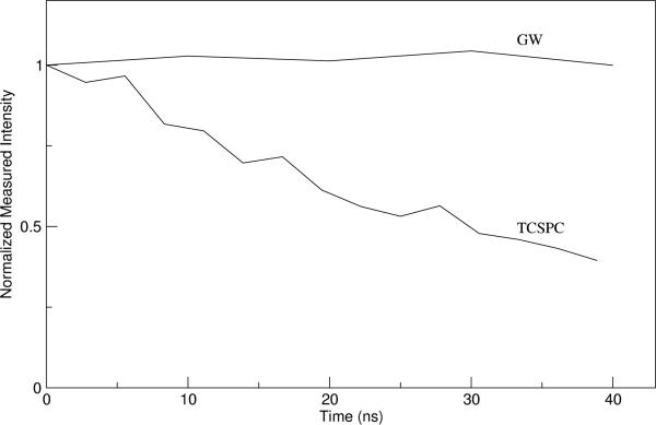
Pile-up nonlinearities do not affect GW mode measurements. To demonstrate this, we measure a constant light source of 3.8 × 10¹⁵ photons/s·cm2 with the imager in both TCSPC and GW modes. This produces approximately 4500 photons per pixel per one hundred TCSPC measurements. At this intensity, pile-up is observed in TCSPC mode as is evident in Fig. 14 due to the obscuring of late-arriving photons by earlier ones leading to a decreasing measured signal beyond the reset time at t = 0. In GW mode, we set Δt = 10 ns and tw ≈ 5 ns. In this case, a constant intensity is observed.
Fig. 14.
Measurement of a constant light source of 3.8 × 10¹⁵ photons/s·cm2 using gated-window (GW) mode and time-correlated single-photon counting (TCSPC) mode
F. Fluorescence Lifetime Measurements
To demonstrate the capability of the imager in both TCSPC and GW modes, we measure the lifetimes of several distinct types of dye. For these measurements, the imager is either mounted on the camera port of an Olympus BX51W1 epifluorescent microscope with a 5× objective or placed in direct proximity to the sample with no intervening optics. The PiLAS gain-switched laser is used to illuminate an area of approximately 4 mm2. The data are fit with exponential decay functions with the appropriate number of components, convolved with the measured IRF corresponding to the measurement mode used. We have focused our initial efforts on fluorophores with relatively long lifetimes—quantum dots, ruthenium-based dyes, and acridine.
1) Quantum dots
Semiconductor quantum dots have several properties which make them excellent fluorescent labels, increasingly adopted in biological research. They are bright and photostable and they can be excited over a large range of wavelengths. On the other hand, the fluorescent decay properties of quantum dots are not well understood [38], [39]. They have been shown to vary across manufacturing lots and to be susceptible to changes in chemical environment [40]. To demonstrate the capabilities of our imager, we have imaged a field of Qdot 655 streptavidin conjugates covalently bonded to epoxy-derivatized glass slides.
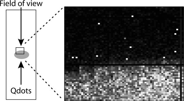
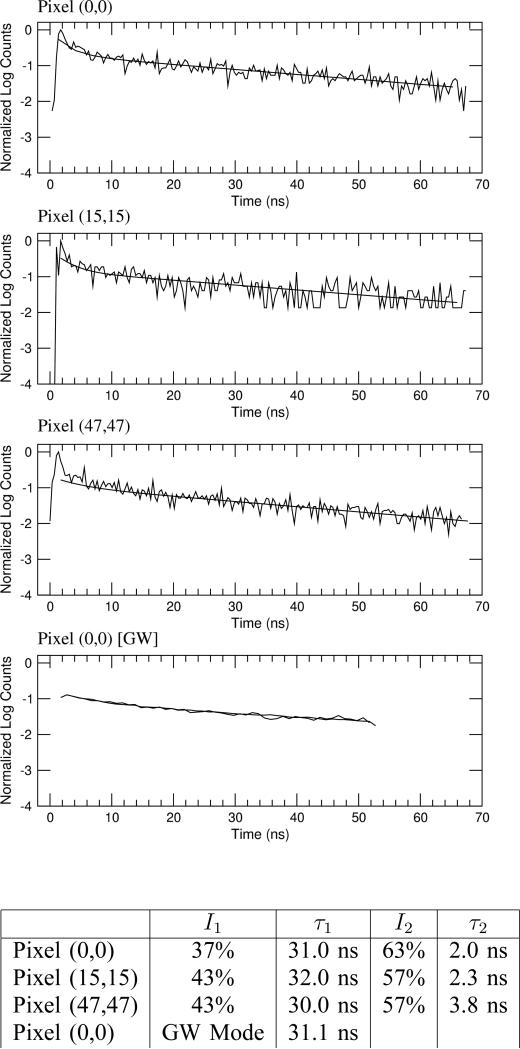
Fig. 15 shows an intensity image of the edge of the region of immobilized Qdot 655 using a filter cube consisting of a 460-nm shortpass emission filter, a 475-nm dichroic beamsplitter, and a 40-nm-wide bandpass emission filter centered at 655 nm. Fig. 16 shows plots of the decay profiles of the quantum dots as measured with three selected pixels on the array using TCSPC mode. The Pixel (0,0) measurement is repeated in GW mode (with Δt = 1 ns and tw ≈ 5 ns) for comparison. The normalized data are fit with a double-exponential decay function, I(t) = I1 exp(t/τ1) + I2 exp(t/τ2), and the resulting lifetime components are shown in the accompanying table in Fig. 16. It is found that, for Qdot 655, the longer lifetime component of the best double exponential fit to the TCSPC mode measurements is fairly consistent over many samples and measurements, and matches the single dominant lifetime of the GW mode measurement, though the shorter lifetime component is highly variable. A single exponential fit, while useful for quick data processing of a highly multiplexed image, shows a high variance.
Fig. 15.
Microscope image of a spot of quantum dots
Fig. 16.
Log plots of Qdot 655 intensity decay as measured in TCSPC mode with three separate pixels and GW mode along with fitted curves
2) A ruthenium complex
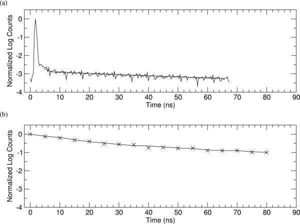
Various complexes of ruthenium(II) have emerged as important markers in biochemical assays. They are triplet emitters with long lifetimes that are sensitive to the oxygen content of their environment [37]. Fig. 17 shows the measured and fit decay curves of tris(1,10-phenanthroline)ruthenium(II) chloride hydrate, dissolved in dimethyl sulfoxide (DMSO) and dried on the surface of a glass slide as measured with the imager in TCSPC mode and in GW mode with tw ≈ Δt = 5 ns. A mono-exponential function fits the data with a lifetime of 69.2 ns in TCSPC mode and 71.1 ns in GW mode.
Fig. 17.
Log intensity plot of a ruthenium complex as measured by the imager in (a) TCSPC mode and (b) GW mode
3) Acridine
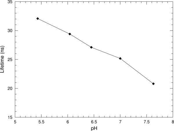
The fluorescent molecule acridine has been shown to have a lifetime that varies with the pH of the solution in which it is dissolved. As such, it is an important example of the utility of lifetime measurement for chemical characterization. Fig. 18 shows the average fluorescence lifetime of 1 mM acridine in 0.1 M sodium phosphate buffer of varying pH as measured with the SPAD imager in TCSPC mode. These results are consistent with those reported in [12].
Fig. 18.
Measured average lifetime of Acridine as a function of pH
V. Conclusion
We have developed a 4096-pixel SPAD array for time-resolved imaging. The imager can be attached to a standard epifluorescent microscope to enable fluorescent lifetime imaging microscopy. We have fully characterized the imager and demonstrated its utility by measuring of the fluorescent lifetimes of semiconductor quantum dots and two traditional fluorophores using both time-correlated single-photon counting and gated-window detection.
Acknowledgment
The authors would like to thank Ike Palka, Jahan Minoo, and especially Frank Zovko and Ping Gong for their assistance with this project.
Appendix
Gated-Window Mode Measurement Linearity
In a gated-window mode measurement, let wi = [ti, ti + tw] be a measurement window, Mi be the number of measurements and H(wi) the number of successful detections with window wi, and Δt be the difference between successive ti. Ĥ(ti) = H(wi)/Mi is, by definition, the measured signal at time ti.
Measurement fidelity is determined by the relationship of the measured signal, Ĥ(ti), to the number of photons that actually arrive during window wi. This latter number is
| (2) |
the integral of the signal intensity over the measurement window, wi = [ti, ti + tw]. In the case that Ĥ(ti)/Ni ≈ C, a constant, the measured intensity in each window will be linearly related to the number of incident photons.
The probability of k photons arriving in an interval [ti, t] can be approximated by the Poisson distribution,
| (3) |
where μi(t) is the mean number of arrivals in [ti, t] [18]. The probability of an arrival in [ti, t] is
| (4) |
and the probability of an arrival in wi is
| (5) |
| (6) |
| (7) |
| (8) |
where (7) depends on the assumption that .
As sensors cannot be gated with infinite slew, their photon detection probability (PDP) is a function of time relative to the nominal window enable time. We denote this function as s(t – ti). Let the probability density function (PDF) of photon arrivals after ti be denoted by
| (9) |
Then the probability of recording a hit in wi is given by
| (10) |
The ensemble average, Ĥ(ti) = Phit(wi), as long as Mi is large. If the PDP is constant (s(t – ti) = s), then Phit(wi) = sParr(wi). From the approximation for Parr in (5)-(8), which is a constant as desired. Even if s(t – ti) is not constant, the integral in (10) will give a weighted average of Parr over wi, with Phit(wi) → s̄Parr(wi) as tw → 0, where , the average of s(t) over a window of width tw.
Because of its impact on linearity in GW measurements, it is important to know the criteria by which the approximation in (7) is valid as, in general, μi(t) is not known. The criterion that μi(t) is small is equivalent to having a low photon flux during wi. Error is accumulated whenever otherwise measurable arriving photons are missed because of the one-count-per-measurement detection limit of the system. Assuming for simplicity that tw is small, this can be formulated as keeping s̄P(k ≥ 2|k ≥ 1) small. Indeed, with the same restriction on μi(t) as above,
| (11) |
| (12) |
| (13) |
| (14) |
Note also that
| (15) |
Error can therefore be minimized by reducing the probability of missing photons, which can be accomplished by reducing the detection rate, Ĥ(wi) = s̄P(k ≥ 1). As in TCSPC mode, a practical rule of thumb is to keep the hits per measurement to around 1%. In TCSPC, this can only be accomplished by attenuating the signal. In GW measurements, however, tw can be diminished to achieve the same result.
Finally, it should be noted that in the above analysis, it has been implicitly assumed that tw ≤ Δt. This validates the approximation of s(t) by s̄ and avoids the spreading of the intensity curve that results from the moving average in (2). Unfortunately, detection systems often have limitations that make it necessary to set tw > Δt, especially when high timing resolution is desired. On the other hand, in the case in which the intensity profile is mono-exponential, measurement linearity is in no way constrained by tw or the PDP function, s(t – ti). In this case, I(t) = I0e–t/τ and μ0(t) = Aτ(1 – e–t/τ), where A is the normalization constant. Furthermore, μi(t) = μ0(t) – μ0(ti) = Aτ(e–ti/τ – e–t/τ).
The requirement that μi(t) be small implies that . So we have,
| (16) |
| (17) |
| (18) |
and Ĥ(ti) ∝ I(ti).
A parallel analysis for a multi-exponential intensity function, , arrives at
| (19) |
| (20) |
Here, the lifetimes are preserved, but their relative weighting is not. This implies that with arbitrary tw, the presence of multiple fluorophores can be detected, but to extract their relative concentrations, it is necessary to have tw ≤ Δt.
Footnotes
Such an intensity is consistent with typical approaches to avoid pile-up in TCSPC [18].
Unfortunately, the sensitivity of the SPADs is degraded by the presence of the transmission gate in the pixel circuit (M6/M7 in Fig. 6a) which clamps the cathode at ~−800 mV through the grounding of the body of M6. The cathode only resets to ~2V. As a result, the excess bias of the diode is limited to approximately 2.7 V. As a larger excess voltage would support a considerably larger PDP, an improved design would eliminate the transmission gate, which is not needed for active pixel operation.
Contributor Information
David Eric Schwartz, Bioelectronic Systems Laboratory, Department of Electrical Engineering, Columbia University, New York, NY 10027 USA (see http://www.bioee.ee.columbia.edu)..
Edoardo Charbon, School of Engineering, Ecole Polytechnique Fédérale de Lausanne (EPFL), 1015 Lausanne, Switzerland.
Kenneth L. Shepard, Bioelectronic Systems Laboratory, Department of Electrical Engineering, Columbia University, New York, NY 10027 USA (see http://www.bioee.ee.columbia.edu)..
References
- 1.Kleinfeld D, et al. Fluctuations and stimulus-induced changes in blood flow observed in individual capillaries in layers 2 through 4 of rat neocortex. Proc. Nat. Acad. Sci. 1998;95(26):15741–15746. doi: 10.1073/pnas.95.26.15741. [DOI] [PMC free article] [PubMed] [Google Scholar]
- 2.Markram H, Sackmann B. Calcium transients in dendrites of neocortical neurons evoked by single subthreshold excitatory postsynaptic potentials via low-voltage-activated calcium channels. Proc. Nat. Acad. Sci. 1994;91(11):5207–5211. doi: 10.1073/pnas.91.11.5207. [DOI] [PMC free article] [PubMed] [Google Scholar]
- 3.Gumbleton M, Stephens DJ. Coming out of the dark: the evolving role of fluorescence imaging in drug delivery research. Adv. Drug Delivery Reviews. 2005;57(11):5–15. doi: 10.1016/j.addr.2004.08.002. [DOI] [PubMed] [Google Scholar]
- 4.Collier T, et al. Real-time reflectance confocal microscopy: comparison of two-dimensional images and three-dimensional image stacks for detection of cervical precancer. J. Biomed. Optics. 2007;12:024021. doi: 10.1117/1.2717899. [DOI] [PubMed] [Google Scholar]
- 5.Piston DW. The coming of age of two-photon excitation imaging for intravital microscopy. Adv. Drug Delivery Reviews. 2006;58(7):770–772. doi: 10.1016/j.addr.2006.07.003. [DOI] [PubMed] [Google Scholar]
- 6.Thompson RB. Fluorescence Sensors And Biosensors. CRC Press; Boca Raton, FL: 2006. [Google Scholar]
- 7.Lakowicz JR. Principles of Fluorescence Spectroscopy. Springer; Berlin: 2006. [Google Scholar]
- 8.Bastiaens PIH, Squire A. Fluorescence lifetime imaging microscopy: spatial resolution of biochemical processes in the cell. Trends in Cell Biol. 1999 Feb.9:48–52. doi: 10.1016/s0962-8924(98)01410-x. [DOI] [PubMed] [Google Scholar]
- 9.Agronskaia AV, et al. Fast fluorescence lifetime imaging of calcium in living cells. J. Biomed. Optics. 2004 Nov-Dec;9(6):1230–1237. doi: 10.1117/1.1806472. [DOI] [PubMed] [Google Scholar]
- 10.Duncan RR, et al. Multi-dimensional time-correlated single photon counting (TCSPC) fluorescence lifetime imaging microscopy (FLIM) to detect FRET in cells. J. Microscopy. 2004 Jul;215(pt. 1):1–12. doi: 10.1111/j.0022-2720.2004.01343.x. [DOI] [PMC free article] [PubMed] [Google Scholar]
- 11.Dumas D, Stoltz J-F. New tool to monitor membrane potential by FRET Voltage Sensitive Dye (FRET-VSD) using Spectral and Fluorescence Lifetime Imaging Microscopy (FLIM) Clin. Hemorheology and Microcirculation. 2005;33:293–302. [PubMed] [Google Scholar]
- 12.Ryder AG, et al. Time-domain measurement of fluorescence lifetime variation with pH. Proc. SPIE. 2001;4259:102–109. [Google Scholar]
- 13.Gerritsen HC, et al. Fluorescence lifetime imaging in scanning microscopes: acquisition speed, photon economy and lifetime resolution. J. Microscopy. 2002 Jun;206(pt. 3):218–224. doi: 10.1046/j.1365-2818.2002.01031.x. [DOI] [PubMed] [Google Scholar]
- 14.Mitchell AC, et al. Measurement of nanoscecond time-resolved fluorescence with a directly gated interline CCD camera. J. Microscopy. 2002 Jun;206(pt. 3):233–238. doi: 10.1046/j.1365-2818.2002.01030.x. [DOI] [PubMed] [Google Scholar]
- 15.Gerritsen HC, et al. High-speed fluorescence lifetime imaging. Proc. SPIE. 2004;5323:77–87. [Google Scholar]
- 16.Schwartz DE, et al. A single-photon avalanche diode imager for Fluorescence Lifetime applications. 2007 IEEE Symp. on VLSI Circuits; Kyoto. 2007.pp. 144–145. [Google Scholar]
- 17.Köllner M, Wolfrum J. How many photons are necessary for fluorescence-lifetime measurements? Chem. Phys. Lett. 1992 Nov.200(1-2):199–204. [Google Scholar]
- 18.Harris CM, Selinger BK. Single-photon decay spectroscopy. II The pile-up problem. Aust. J. Chem. 1979;32:2111–2129. [Google Scholar]
- 19.Coates PB. The correction for photon ‘pile-up’ in the measurement of radiative lifetimes. J. Phys. E: Scientific. Inst. 1968;1:878–879. [Google Scholar]
- 20.Walker JG. Iterative correction for ‘pile-up’ in single-photon lifetime measurement. Optics Comm. 2002 Jan.201:271–277. [Google Scholar]
- 21.Ballew RM, Demas JN. An error analysis of the rapid lifetime determination method for the evaluation of single exponential decays. Analytical Chemistry. 1989;61(1):30–33. doi: 10.1021/ac981050d. [DOI] [PubMed] [Google Scholar]
- 22.Sharman KK, et al. Error analysis of the rapid lifetime determination method for double-exponential decays and new windowing schemes. Analytical Chemistry. 1999;71(5):947–952. doi: 10.1021/ac981050d. [DOI] [PubMed] [Google Scholar]
- 23.Kindt WJ, Van Zeijl HW. Modelling and fabrication of Geiger mode avalanche photodiodes. IEEE Trans. on Nucl. Sci. 1998;45(3):715–719. [Google Scholar]
- 24.Rochas A, et al. Single photon detector fabricated in a complementary metal-oxide-semiconductor high-voltage technology. Review Sci. Inst. 2003 Jul;74(7):3263–3270. [Google Scholar]
- 25.Niclass C, et al. A single photon avalanche diode implemented in 130-nm CMOS technology. IEEE J. of Sel. Topics in Quantum Electron. 2007;13(4):863–869. [Google Scholar]
- 26.Marwick MA, Andreou AG. Fabrication and testing of single photon avalanche detectors in the TSMC 0.18μm CMOS technology. 41st Annual Conference on Info. Sci. and Systems; Baltimore, MD. 2007.pp. 741–744. [Google Scholar]
- 27.Filkelstein H, et al. Performance trade-offs in single-photon avalanche diode miniaturization. Review of Sci. Instruments. 2007;78:103103. doi: 10.1063/1.2796146. [DOI] [PubMed] [Google Scholar]
- 28.Cova S, et al. Evolution and prospects for single-photon avalanche diodes and quenching circuits. J. Mod. Optics. 2004 Jun-Jul;15(9-10):1267–1288. [Google Scholar]
- 29.Räisänen-Ruotsalainen E, et al. Time interval measurements using time-to-voltage conversion with built-in dual-slope A/D conversion. IEEE International Symp.on Circ. and Syst. 1991;5:2573–2576. [Google Scholar]
- 30.Moyer GC, et al. Precise delay generation using the Vernier technique. Electronics Lett. 1996;32(18):1658–1659. [Google Scholar]
- 31.Henzler S, et al. Variation tolerant high resolution and low latency time-to-digital converter. 33rd European Solid State Circuits Conf.; Munich. 2007.pp. 194–197. [Google Scholar]
- 32.Chappell BA, et al. Fast CMOS ECL receivers with 100-mV worst-case sensitivity. IEEE J. Solid-State Circuits. 1988;21(1):59–67. [Google Scholar]
- 33.Sidiropoulos S, et al. Adaptive bandwidth DLLs and PLLs using regulated supply CMOS buffers. 2000 Symp. on VLSI Circuits Dig. of Tech. Papers.pp. 124–127. [Google Scholar]
- 34.Spinelli A, Lacaita AL. Physics and Numerical Simulation of Single Photon Avalanche Diodes. IEEE Trans. on Electron Dev. 1997;44(11):1931–1943. [Google Scholar]
- 35.Ripamonti G, Cova S. Carrier diffusion effects in the time-response of a fast photodiode. Solid-State Electronics. 1985;28(9):925–931. [Google Scholar]
- 36.Cova S, et al. Trapping phenomena in avalanche photodiodes on nanosecond scale. IEEE Electron Dev. Lett. 1991 Dec.12(12):685–687. [Google Scholar]
- 37.Nair RB, et al. Optical properties of [Ru(phen)2dppz]2+ as a function of nonaqueous environment. Inorg. Chem. 1997;36:962–965. doi: 10.1021/ic960862u. [DOI] [PubMed] [Google Scholar]
- 38.Kapitonov AM, et al. Luminescence properties of thiol-stabilized CdTe nanocrystals. J. Phys. Chem. B. 1999;103:10109–10113. [Google Scholar]
- 39.Schlegel G, et al. Fluorescence decay time of single semiconductor nanocrystals. Phys. Rev. Lett. 2002 Apr.18(3) doi: 10.1103/PhysRevLett.88.137401. [DOI] [PubMed] [Google Scholar]
- 40.Yao J, et al. Blinking and nonradiant dark fraction of water-soluble quantum dots in aqueous solution. Proc. Nat. Acad. Sci. 2005 Oct.102(40):14284–14289. doi: 10.1073/pnas.0506523102. [DOI] [PMC free article] [PubMed] [Google Scholar]


