

Focused ion beam (FIB) fabrication of fiber optic sensors, mainly chemical sensors, which are based on plasmonics-active nanostructures formed on the cleaved tips of optical fibers, are reported. The nanostructures fabricated included nanoholes in optically thick metallic films as well as metallic nanopillars and nanorods. The sensing mechanism is based on detecting shifts in surface plasmon resonances (SPR) associated with nanoholes in metallic films and localized surface plasmon resonances (LSPRs) of metallic nanopillars and nanorods, when the refractive index of the medium surrounding the nanostructures is changed. These sensors can be employed for the detection of chemical agents in air as well as liquid media surrounding the sensors. FIB milling was employed to fabricate ordered arrays of nanoholes in optically thick (100–240 nm) metallic films deposited on cleaved end-faces of multimode, 4-mode, and single mode optical fibers. Separately, metallic nanorods and nanopillars were formed by first depositing a a metallic (gold or silver) film on tips of optical fibers which was followed by FIB milling large area patterns to form freestanding nanorods and nanopillars. Utilizing FIB allows engineering nanostructure geometries, i.e. nanostructure shapes and sizes that are chosen based on the plasmon resonances associated with them. Formation of periodic arrays of nanoholes provides a means of tuning plasmon resonance peaks, associated with extraordinary transmission of light through the array of nanoholes in the metallic films, based on periodicity and shape of the nanoholes as well as on refractive index changes to form sensitive chemical sensors
I. INTRODUCTION
Development of sensors on optical fibers makes these sensors portable, allows remote sensing and creates the ability to embed these sensors in flexible substrates. In our work, optical fiber based nanosensors were applied for the detection of chemical molecules surrounding the sensors. Focused ion beam (FIB) milling was utilized to pattern nanostructures such as nanopillars, nanorods, and nanoholes from 30–200 nm thick metallic films deposited on the tips of optical fibers. This process allows nano-scale control of dimensions of the metallic structures fabricated on the fiber tips enabling us to develop plasmon resonance based sensors with control on the spectral position of these resonances. Moreover, FIB allows these sensors to be developed in a reproducible manner with relative ease. We describe the development of FIB fabrication procedures to form metallic nanostructures having sizes less than 100 nm and non-circular cross-sectional shape. The focus of this paper is on developing and fine-tuning fabrication procedures for FIB milling of metallic nano nanostructures on the tips of optical fibers, while sensing data that demonstrate the viability of these sensors to be used as chemical sensors are also presented.
Surface plasmons1–7 are defined as collective oscillations of the conduction band electrons on the surface of continuous thin metallic films, on metallic films containing gratings or nanohole arrays, or on confined nanostructures such as nanopillars or nanorods. In the case of the confined nanostructures, surface plasmons are known as localized surface plasmons (LSPs).3–7 While surface plasmons in continuous thin metallic films are excited by radiation of certain wavelengths that are incident at certain angles, thin films having gratings and nanohole arrays allow coupling of normally incident light to surface plasmons. LSPs can be excited by normally incident light on confined nanostructures or an array of these nanostructures that have a size much smaller than the wavelength of the incident light.3–7 Surface plasmons can be detected as resonance peaks in the transmission, reflection, absorption or scattering spectra of the metallic nanostructures and films. Nanostructures and films of noble metals like gold, silver, and copper exhibit surface plasmon excitation in the visible and near-infrared spectral region and are materials of choice for plasmon related sensors.2–7
In our study, fiber optic sensors were developed that exploited plasmon resonances associated with thin metallic films having periodic nanohole arrays9–13 - mainly surface plasmon resonance (SPR), as well as those associated with metallic nanopillars and nanorods termed Localized Surface Plasmon Resonances (LSPRs).3–7 Both configurations allow excitation of plasmons by light propagating through the fiber that is incident normally on these nanostructures. Moreover, unlike the continuous thin film SPR2, polarization and angle of incidence requirements are relaxed in these structures. Bethe8–9 discussed the transmission of light through apertures smaller than the wavelength of the incident light – when no surface plasmon excitation is considered - and demonstrated that the transmission of light through an aperture is proportional to (r/λ)4 and is negligible when the radius of the aperture is smaller than the wavelength of the incident light. Excitation of surface plasmons on the surface of an optically thick plasmonically-active metallic film (such as a gold or silver film), having an array of nanoapertures, enhances the transmission of light through the nanoapertures in the film at certain wavelengths.9–13 The wavelengths at which there is enhanced transmission of light through the nanohole array are a function of the periodicity of the nanoholes in the array, which should be less than the propagation distance of the plasmons on the metal surface, and material parameters. The relationship between the wave vector of the surface plasmon waves kSP, the in-plane component of the wave vector of the incident light kx, and the allowed momentum vectors of the periodic structure Px and Py is given by Equation (1). Bloch’s theorem and the periodicity of the structure restrict the allowed momentum vectors to integer multiples i and j, which correspond to the (i, j) diffraction order associated with the light transmission through the periodic nanohole array.9–13 The magnitudes of Px and Py are 2π/Lx, and 2π/Ly respectively, where Lx and Ly are the periodicities of the nanoholes (When the nanoapertures are spaced equally in the × and y directions, Lx = Ly = L) in the × and y directions in the plane of the metallic film.
| (1) |
For light incident normally on the nanohole array, the magnitude of the vector kx is zero. For light incident normally on the nanohole array, the magnitude of the vector kx is zero. The shapes of nanoapertures in the array also contribute to the plasmon resonance excitation in the nanohole arrays via shape-dependent localized surface plasmon resonance (LSPR) effects. The surface plasmons are excited on both surfaces of the optically thick metallic film containing the nanohole array and Equation (2), defines the magnitude of the wave vector of the surface plasmon waves’
| (2) |
where εmetal and εs are the dielectric constants of the metal and the surrounding dielectric medium, respectively and εmetal is a complex number dependent on wavelength of the incident radiation. Therefore, the position of the peaks associated with the extraordinary transmission of light through the nanohole arrays depends on the refractive index of the media on either side of the metallic film. When the refractive index of the media next to the gold film containing the array of nanoholes changes, a shift in the peaks in the optical spectra of light transmitted through the array is observed. Hence, these nanohole array containing metallic films can be employed to form sensors to detect the changes in refractive index of the media on either side of the metallic film containing the nanohole array.
II. FABRICATION OF THE NANOSENSORS AND EXPERIMENTAL
The optic fiber based nanosensors were fabricated by FIB patterning of nanopillars, nanorods, and sub wavelength holes from a metallic film deposited on the cleaved tips of optical fibers tips. Preparation of the optical fibers used in this work involved stripping the polymer jacket with a fiber stripper and cleaving the stripped fiber with a fiber cleaver to obtain a flat fiber end-face. The single mode and four mode fibers employed in this work had core diameters of 4 μm and 8 μm respectively, with the cladding diameter being 125 μm for both types of the fibers. The graded-index fibers were obtained from 3M and had a 62.5 μm core and a 125 μm cladding diameter.
After lightly etching the cleaved fiber faces, to make core identification easier, electron beam evaporation was used to coat the fiber tips with 120–250 nm of gold for the films having arrays of nanoapertures and 30–100 nm of gold for the films having arrays of other nanostructures such as nanopillars and nanorods. The thickness of the gold film was monitored by a quartz crystal monitor. A Hitachi FB2100 Focused Ion Beam milling system with a gallium ion source was used to fabricate the arrays of nanoapertures and other nanostructures such as nanopillars and nanorods. A 40 keV beam was used for fabrication. The desired array of nanostructures was milled by rastering the ion beam and employing beam blanking. An 8 bit grayscale, 512 × 512 pixel image file defined the desired patterned array. Arrays of nanoapertures measuring 8 × 8, 12 × 12 and 24 × 24 microns were fabricated onto the core of the gold-coated optical fibers. The nanostructures formed on the tips of optical fibers by FIB were evaluated for their diameter, height, and shape by employing both scanning ion microscopy (SIM) and scanning electron microscopy (SEM). Characterization of the as fabricated nanosensors was achieved by employing white light (400–760 nm) from a tungsten halogen lamp incident onto one end of the optical fiber. The light propagated through the optical fiber and was incident on the nanohole array and the nanostructures. We employed a collector optical fiber, placed at a distance of ~ 350 microns from the end-face of the nanosensor fiber, to collect the light transmitted through the nanohole arrays or the array of other nanostructures such as nanorods and nanopillars. Optical transmission measurements on the gold-coated optical fibers were made using a SpectraPro®-500, ¼ meter spectrometer with a 600 line per inch grating and a Peltier cooled CCD array. The effect of changing the refractive index of the medium around the optical fiber probe tip was quantified by inserting the sensor and collector fibers in a sensor chamber such that the fibers were kept aligned as the liquids of different refractive indices were tested.
III. RESULTS AND DISCUSSION
Fig. 1 shows SIM secondary electron (SE) micrographs of gold nanopillar arrays, FIB fabricated, on the tips of cleaved optical fibers. Fig. 1(a) shows an 8 × 8 nanopillar array on the tip of a 50 nm gold coated 4-mode optical fiber, having an 8 μm diameter core region. In this optical fiber, the bulk of the gold film was milled from the core region of the optical fiber leaving gold nanopillars. This enables minimizing the interaction of light propagating in the core region of the optical fiber with the continuous gold film (50 nm thick) so that the majority of the light propagating in the core region of the fiber interacts with the nanopillars and nanorods on the optical fiber end-face. The interaction of light with the continuous gold film results in a peak, corresponding to interband transitions in the 50 nm gold film, in the transmission spectrum. This peak could have an overlap with the LSPR-related dips in the transmission spectrum of the nanorods and nanopillars formed on the optical fiber tip and could thereby obscure the LSPR signal. Fig. 1(b) shows multiple 4 by 4 nanopillars regions on the tip of a multi-mode optical fiber coated with 200 nm gold. Although light propagating in the 100 micron diameter core region of the optical fiber does interact with the gold film, the 200 nm thickness of the gold film blocks most of the light propagating through the gold film which results in a lower peak corresponding to interband transitions in the gold film in the overall transmission spectrum of the optical fiber. The gold nanopillars are thinned down to the desired height (~ 50 nm) from the original 200 nm thickness of the gold film by employing a defocused ion beam scanned over the array region. In Fig. 1, the dark regions show the silica optical fiber background where as the lighter regions are the gold film and the nanopillars milled from this film. Figs. 1(c)-(f) show SIM micrographs of gold nanopillar arrays of square, elliptical, triangular, and circular geometries, formed on tips of optical fibers.
Fig. 1.
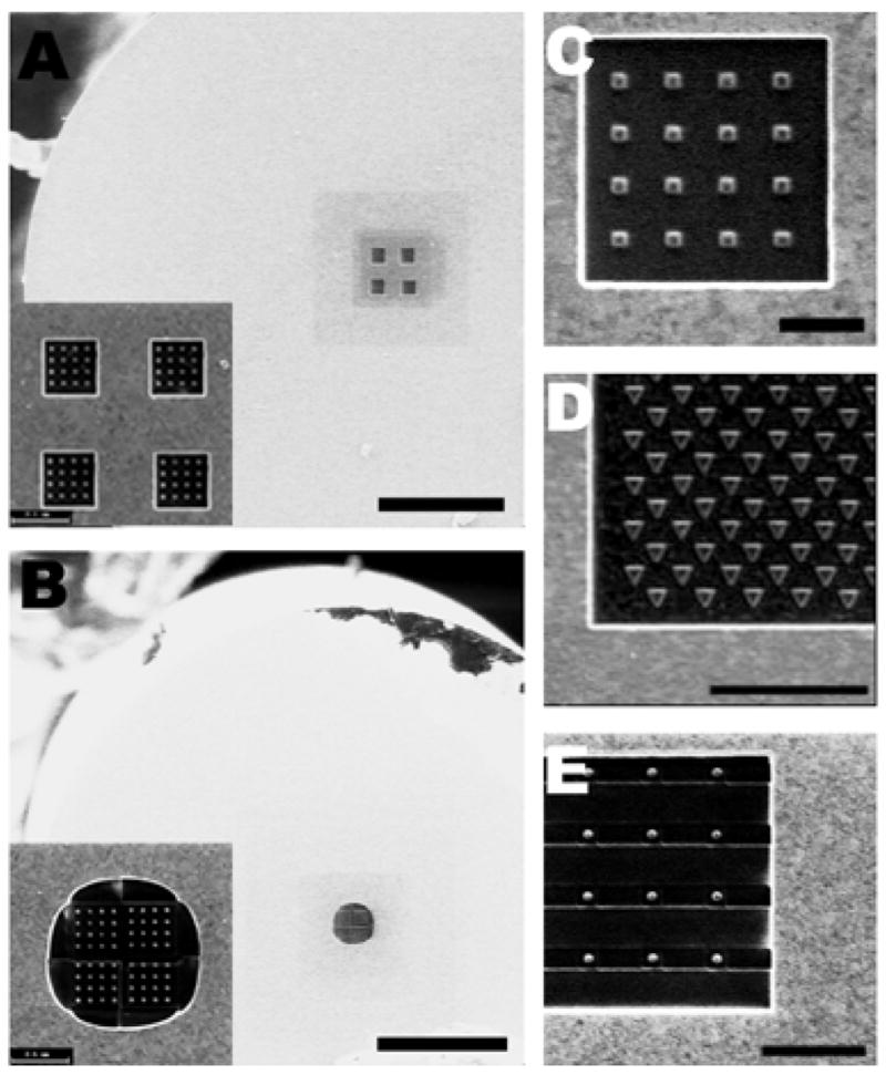
A. Multiple 4 × 4 nanopillars regions on the tip of a multi-mode optical fiber coated with a 200 nm gold layer. Scale bar is 20μm. Inset shows higher magnification of nanopillar array. B. Scanning ion microscope (SIM) image of a 8 × 8 square nanopillar array, developed by FIB, at the tip of a 50 nm gold coated 4-mode optical fiber. Scale bar is 20μm. Inset shows higher magnification of pattern located on center of fiber. C. Higher magnification of a 4 × 4 square-shaped gold nanopillar array, developed by FIB. Scale bar is 1 μm. D. Triangular FIB machined array. Scale bar is 2.5 μm. E. Circular nanopillar arrays formed by FIB milling of a 60 nm thick gold film. Scale bar is 2.5 μm.
In order to form nanostructures below 60–80 nm side dimensions, a two step fabrication process was followed. The first step involved forming nanostructures of larger dimensions (nanostructure length and width) followed by a second step to trim the dimensions down to the desired dimensions. Fig. 2(a) shows a SIM micrograph of a 4 by 4 square nanopillar array FIB fabricated on the tip of a multimode optical fiber having a 50 nm thick gold film on its tip. The first and second elements of the nanopillar array show how particles of smaller size and the desired shape can be formed by employing a first step involving formation of a nanopillar array consisting of particles of larger size (200 nm by 200 nm) and then employing a second milling step to form nanopillars of the desired size and shape. Fig. 2(b) shows how triangular-shaped nanopillars can be formed by the above method. The nanopillars shown in Fig. 2(b) have side lengths of ~ 80 nm. Fig. 2(c) shows how an array of nanorods can be formed on the tip of a 4-mode optical fiber by employing FIB. The top 4 rows in Fig. 2(c) show how milling for a larger duration can be carried out to reduce the height of the nanorods to the desired height of 80 nm from the original pillar height of 200 nm. This mechanism can also allow pillars of multiple heights to be present on the tip of the optical fiber sensor.
Fig. 2.

A. SIM micrograph of 4 × 4 square nanopillar array, developed by FIB, at tip of a 50 nm gold coated multimode optical fiber. The first and second elements of the nanopillar array show how particles of smaller size and the desired shape can be formed by employing a first step involving formation of a nanopillar array consisting of particles of larger size (200 nm by 200 nm) and then employing a second step to form nanopillars of the desired size and shape. Scale bar is 2 μm. B. Triangular-shaped nanopillars formed by the above method. Scale bar is 1 μm. C. 8 × 8 array of nanorods formed on the core of a 4-mode fiber coated with a 200 nm thick Au layer. The height of the nanorods can be thinned down to the desired height (80 nm) after the first stage of nanorods formation as is shown in the top 4 rows of the nanorods array. Scale bar is 2.5 μm. D. SEM micrograph, taken at a 30 degree tilt, showing an array of gold nanopillars formed by FIB. Scale bar is 1 μm. E. Higher magnification SEM image of the nanopillars shown in D. Scale bar is 500nm.
Figs. 2(d) and 2(e) show SEM micrographs obtained at 100,000X magnification of gold nanopillars formed by FIB obtained by tilting the fiber tip containing the nanopillars. This enables estimation of the actual height of the nanorods and nanopillars after the FIB milling process to form the nanostructures. During FIB milling gold film material milled from certain regions re-deposited on some other sections from where gold was milled. In those cases, another step of FIB milling was carried out until the nanopillars in the array were surrounded by a dark background indicating the removal of all gold material from those sections. Much of the work described in this paper was focused on fabrication of gold nanopillars on tips of optical fibers and future work will involve further characterization of these optical fiber sensor probes for LSPR-based chemical sensing applications.
In further work, periodic arrays of nanoapertures were formed on the tips of metal-coated optical fibers were fabricated and these optical fibers employed for chemical sensing applications. In order to study the effect of nanoaperture shape and gold film thickness, fiber samples with metallic films having different nanoaperture shapes as well as different film thicknesses were fabricated and evaluated. Figs. 3(d)–(g) show SIM micrographs of arrays of nanoapertures, having circular, rectangular, triangular, and elliptical shapes in a 180 nm gold film deposited on the tip of an optical fiber. Periodicity of the nano-apertures in these arrays was 600 nm and the individual nanoapertures had the same cross-sectional area for the holes of different shapes. In order to test the repeatability of the transmission measurements through the different metal-coated optical fiber tips containing the nanoaperture arrays, 4 fiber samples of each kind (nanoaperture geometry and gold film thickness) were developed and evaluated. Fig. 3(a) shows an SIM micrograph of a multimode fiber having a 24 by 24 periodic array of circular nanohole arrays on its gold-coated tip. Process optimization lead to the development of nearly uniform holes. Fig. 3(b) shows a 48 by 48 nanohole array formed on the tip of a multimode optical fiber. Fig. 3(c) shows a 8 by 8 periodic array of triangular nanoapertures fabricated in a gold film coated tip of 4-mode optical fiber, having a 8 μm core diameter and a 125 μm cladding diameter. The nanoaperture array covered the entire core region of the optical fiber, which allows more interaction of light propagating in the optical fiber with the array of nanoapertures in the optically thick gold film deposited on the fiber tip. Transmission spectrum of a 24 by 24 array of circular apertures, in a 180 nm thick gold film deposited on the tip of an optical fiber is shown in Fig 4(a), where one can observe a peak at ~ 500 nm due to electron transitions between the d-bands in the metal and the Fermi level in conduction band. This peak is characteristic of the gold layer and is not dependent on the shape or size of the nanohole array or on the refractive index of the surrounding medium. The second and third peaks in Fig. 4(a) are present due to the excitation of surface plasmons in the gold film and are dependent on the structure of the nanohole array, size and shape of the nanoholes, thickness of the gold film, and refractive index of the media on either side of the nanohole array. One can attribute the peak at ~ 600 nm in Fig. 4(a) to the (1, 0) scattering order - this is determined based on equation 2 employing the Drude model to determine the value of wavelength dependent dielectric constant of the metal i.e. εmetal (λ) such that values of the constants employed are consistent with optical constant values provided by Palik14 for different wavelengths (λ) - of a circular nanohole array grating with air as the medium next to the gold film. The data shown in Figure 4(a) corresponds to the nanohole array shown in Figure 3D: individual hole diameter being 200 nm, the gold film thickness being 180 nm, and the periodicity of the holes in the array being 600 nm. Based on the calculations using equation 2, the peak at 660 nm in Fig. 4(a) is ascribed to the (1, 1) scattering order with silica as the surface adjacent to the gold film containing the nanohole array.
Fig. 3.

A. SIM micrograph showing nanoaperture arrays formed on the gold-coated tip of cleaved end-face of a step-index multimode fiber with a diameter of 125 μm and a periodic array of 24 × 24 nanoholes. B. Core region of a 4-mode optical fiber with an aligned triangular nanohole array created by FIB milling. Scale bar is 2.5 μm. C. A 24 × 24 nanohole array formed on the tip of a multimode optical fiber. Scale bar is 4.5 μm. D. Gold film having periodic array of nanoapertures on the cleaved tip of multimode fiber. These nanoapertures have diameters ~200 nm. E. Rectangular FIB mills created this nanohole array. Scale bar is 1.5 μm. F. Elliptical nanoholes in an array. Scale bar is 2 μm.
Fig. 4.

Transmission spectrum of a 24 × 24 nanohole array in a gold film 180 nm thick, on the tip of a multimode optical fiber, the spacing between the nanoholes in the array being 600 nm. The nanohole geometries were Circular (A) and Rectangular (B). C. Transmission spectra of a 230 nm gold film having a 24 × 24 square nanohole array on the tip of a multimode fiber, evaluated in the wavelength range of 460–720 nm upon changing the medium surrounding the fiber tip from Air (L), Methanol (M), then Air (N) again after Methanol evaporation drying, and (O) Methanol added again to the sensor chamber. The spacing between the holes was ~ 620 nm. (D) Dependence of the (1, 0) scattering order peak in the transmission spectra of a 230 nm gold film, having a 24 × 24 square nanohole array on the tip of a multimode fiber, on the refractive index of the medium around the fiber tip.
Fig. 4(b) shows the transmission spectrum of an array of rectangular nano-apertures on the tip of a gold film-coated multimode optical fiber, the thickness of the gold film being 180 nm. This figure shows a broad peak between 640 nm and 690 nm instead of the sharper peaks present in the transmission spectrum shown in Fig. 4(a), which is associated with circular nanoholes. In arrays of rectangular nanoapertures, both the effect of nanoaperture shape resonances and localized surface plasmons, excited along the long and short edges of the rectangular aperture, as well as the surface plasmon modes due to the periodic array of nano-apertures have an effect on the transmission spectrum. The data shown in Figure 4(b) corresponds to the nanohole array shown in Figure 3E: individual nanohole dimensions being 200 nm by 157 nm, the gold film thickness being 180 nm, and the periodicity of the holes in the array being 600 nm. Degiron et al.9 showed that the localized surface plasmons excited in rectangular nano-apertures are polarization-dependent, and different plasmon resonance related peaks are obtained if the incident light is polarized along edges of the rectangular apertures in the array. As unpolarized light was employed in our evaluation of the rectangular nanoaperture arrays, the broad plasmon resonance related peak between 640 nm and 690 nm in Fig. 4(b) is attributed to the superposition of two peaks due to excitation of localized surface plasmons along the long (200 nm long) and short edges (157 nm long) of the nano-apertures. Fig. 4(c) shows the transmission spectrum of a 24 by 24 nanohole array in a 230 nm gold film on the tip of a multi-mode optical fiber with air and methanol being he media on one side of the gold film containing the nanohole array and silica optical fiber being the media on the other side of the film. Dimensions of the individual nanoholes in this array were ~ 200 nm and the periodicity of the holes in the array was ~ 620 nm. As sharp plasmon related peaks in the transmission spectra were obtained for the case of this optical fiber sensor, this sensor configuration was investigated for its application as a refractive index based chemical sensor. The optical fiber sensors were evaluated for shifts in SPR related peaks in transmission spectra as the refractive index around the fiber tip is varied. An example of a change in the transmission spectrum, upon changing the refractive index of the medium around the sensor tip, is shown in Fig. 4(c) where there was a change in the transmission spectrum as the medium surrounding a multimode fiber tip, was changed from air with refractive index ~ 1.00029 to methanol with refractive index ~ 1.33. It is observed that the peak which was observed at 637 nm in air is shifted to 672 nm in methanol. This can be attributed to the fact that the peak at 637 nm corresponds to the (1, 0) diffraction order of the nanohole array grating (based on calculations using equation 2) when the nanohole array is surrounded by air and this peak moves to a higher wavelength when methanol is inserted around the nanohole array. It can also be observed from Fig. 4(c) that when methanol is removed and air surrounds the tip of the fiber sensor, the transmission spectrum is almost identical to the spectrum before methanol was added, with the (1, 0) diffraction order peak going back to its original position. Moreover, it can be observed from Fig. 4(c) that when methanol is added back again, the transmission spectrum is almost identical to the spectrum before methanol was dried, with the (1, 0) diffraction order peak going back to its original position. The effect of changing refractive index of the medium, by employing fluids of different known refractive indices, surrounding the fiber tip sensor region was investigated by taking transmission measurements of the fiber sensors in different media and the results are presented in Fig. 4(d). One can observe from Fig. 4(d) that there a large shift (~ 24 nm) in the spectral position of the peak associated with the (1, 0) scattering order in the transmission spectrum of the circular nanohole array - when the refractive index of the medium surrounding the optical fiber was varied from 1.33 to 1.376. This illustrates high sensitivity levels ~ 500 nm/RIU (Refractive Index Unit) of this class of sensors for detecting changes in the bulk refractive indices associated with the different chemicals surrounding the sensor.
IV. CONCLUSIONS
FIB fabrication of plasmonics-active nanostructures on cleaved tips of the optical fibers is suitable for chemical sensing applications has been demonstrated. The metallic nanostructures fabricated included nanopillars, nanorods, and nanoholes in optically thick metallic films, mainly gold and silver films. Employing FIB milling for nanostructure formation allows precise control of nanostructure size and shape. Multi-step FIB fabrication procedures were developed to form the nanostructures of different sizes and shapes on tips of optical fibers. The development of sensitive chemical sensors on optical fiber tips containing periodic arrays of nanoholes in optically thick metallic films deposited on the tips is demonstrated. Sensing mechanism in these sensors was based on detecting shifts in the SPR-related peaks in the transmission spectra of nanoholes in the metallic films, when the refractive index of the medium surrounding the nanoholes was varied.
Acknowledgments
The authors would like to thank the sponsors of this work - U. S. Army Research Office, National Research Council (NRC), and the National Institutes of Health (Grants R01 EB006201 and R01 ES014774), and Hitachi High Technologies America for technical support.
References
- 1.Raether H. Surface plasmons on smooth and rough surfaces and on gratings. Springer Verlag; Berlin: 1988. [Google Scholar]
- 2.Slavik R, Homola J, Ctyroky J. Sens Actuators B. 1999;54:74. [Google Scholar]
- 3.Haes AJ, Van Duyne RP. Anal Bioanal Chem. 2004;379:920. doi: 10.1007/s00216-004-2708-9. [DOI] [PubMed] [Google Scholar]
- 4.Okamoto T. In: Near-Field Optics and Surface Plasmon Polaritons. Kawata S, editor. Springer-Verlag Berlin; Heidelberg: 2001. [Google Scholar]
- 5.Mock JJ, Smith DR, Schultz S. Nano Lett. 2003;3:485. [Google Scholar]
- 6.Dhawan A, Muth JF. Nanotechnol. 2006;17:2504. doi: 10.1088/0957-4484/17/10/011. [DOI] [PubMed] [Google Scholar]
- 7.Mcfarland AD, Van Duyne RP. Nano Lett. 2003;3:1057. [Google Scholar]
- 8.Bethe HA. Phys Rev. 1944;66:163. [Google Scholar]
- 9.Degiron A, Ebbesen TW. J Opt A: Pure Appl Opt. 2005;7:590. [Google Scholar]
- 10.Barnes WL, Dereux A, Ebbesen TW. Nature. 2003;424:824. doi: 10.1038/nature01937. [DOI] [PubMed] [Google Scholar]
- 11.Dintinger J, Klein S, Ebbesen TW. Adv Mater. 2006;18:1267. [Google Scholar]
- 12.Lezec HJ, Thio T. Opt Express. 2004;12:3629. doi: 10.1364/opex.12.003629. [DOI] [PubMed] [Google Scholar]
- 13.Dhawan A, Gerhold MD, Muth JF. IEEE Sens J. 2008;8:942. [Google Scholar]
- 14.Palik ED. Handbook of Optical Constants of Solids. Academic; San Diego, Calif.: 1998. [Google Scholar]