

Abstract
This paper describes the fabrication of gold nanopillar and nanorod arrays and theoretical calculations of electromagnetic fields (EMFs) around ordered arrangements of these nanostructures. The EMFs of both single nanopillars and di-mers of nanopillars - having nanoscale gaps between the two adjacent nanopillars forming the di-mers - are simulated in this work by employing the Finite Difference Time Domain (FDTD) method. In the case of simulations for di-mers of nanopillars, the nano-scale gaps between the nanopillars are varied between 5 nm and 20 nm and calculations of the electromagnetic fields in the vicinity of the nanopillars and in the gaps between the nanopillars were carried out. Fabrication of gold nanopillars in a controlled manner for forming SERS substrates involves focused ion beam (FIB) milling. The nanostructures were fabricated on gold-coated silica, mica, and quartz planar substrates as well as on gold-coated tips of four mode and multimode silica optical fibers.
1.0 Introduction
The enhancement of electromagnetic fields in the vicinity of the metallic nanoparticles is important for the development of both localized surface plasmon resonance (LSPR) [1-4] based and surface-enhanced Raman scattering (SERS) [5-9] based sensors. In the case of LSPR-based sensors, the shape and magnitude of the dip in the transmission spectra depend on the enhanced scattering and absorption of light at specific wavelengths, which depends on the geometry of nanostructures illuminated by the light. The origin of plasmon resonances of metallic nanoparticles are collective oscillations of the conduction band electrons in the nanoparticles. These oscillations are called localized surface plasmons, which are excited when light is incident on metallic nanoparticles that have dimensions smaller than the wavelength of the incident light. At certain wavelengths, resonant multipolar modes are excited in the nanoparticles, leading to significant enhancement in absorbed and scattered light and strong increase in the electromagnetic fields in the vicinity of the particles. Localized surface plasmons can be detected as resonance peaks in the absorption and scattering spectra of the metallic nanoparticles [10-12]. Noble metal nanoparticles, mainly gold and silver nanoparticles resonantly scatter and absorb light in the visible and near-infrared spectra. Excitation of localized surface plasmons and an increase in the localized electric and magnetic fields in the vicinity of the metallic nanoparticles are dependent on the shape and size of the nanoparticles, with higher fields observed in metallic nanoparticles having non-spherical geometries such as triangular or ellipsoidal nanoparticles as well as in the spacing between the metallic nanoparticles. The enhancement of electromagnetic field intensity inside and near metallic nanoparticles, due to excitation of localized surface plasmons in the particles, is estimated to be greater than that of surface plasmon resonance in continuous thin films. These high electromagnetic fields around the nanostructures also lead to higher SERS signals obtained from the region containing these nanostructures as compared to the SERS signals obtained without the structures [13-17]. Intensities of the SERS peaks are dependent on the nanostructure geometry and the spacing between the nanostructures. Along with the LSPR effect, one can achieve high EM enhancement by producing “nano-antenna” effects occurring in the nano-scale spacing between nanostructure pairs.
The objectives of this research are to estimate and predict electromagnetic enhancement of SERS by theoretical calculations using FDTD and fabricating metallic nanostructures in a controlled manner on solid substrates. Based on the theoretical calculations and the models developed, we designed and fabricated efficient plasmonics-active nanostructures for achieving optimal EM enhancement in the SERS signals. There are two main sources of electromagnetic enhancement of SERS - The first part of the enhancement is due to excitation of surface plasmons or electronic vibrations on the SERS substrate having a nanostructured metallic surface, which leads to significant enhancement in the localized electromagnetic fields in the vicinity of the substrate. EM enhancement also occurs due to plasmonic amplification of Raman signals emanating from the SERS-active molecules attached to the substrate. Hence, the overall enhancement of SERS is proportional to the fourth power of the field at the molecule [16-17].
Finite-Difference Time-Domain (FDTD) algorithms [18-20] analyze structures by solving the differential form of coupled Maxwell's equations. They can be used for the analysis (e.g., determination of electric and magnetic field distribution, energy and power distribution, etc.) of metallic nanoparticles, nanorods, nano-apertures and other nanostructures on planar substrates, in liquid media, in or on the surface of waveguides, etc. The FDTD method involves discretization of the Maxwell's equations in both time and the space domains in order to find the E and H fields at different positions and at different time-steps. An FDTD algorithm, called the Yee's algorithm [18] is employed to determine fields at different points in space at different times. In an FDTD lattice or grid, every E component is surrounded by four H components and every H component is surrounded by four E components. In our work, the FDTD analysis incorporates the effects of dispersion relations, i. e. the effects of wavelength dependence (e.g., appropriate dispersion relation such as Debye, Lorentz, etc.) of the dielectric constants of the metallic media.
Focused ion beam (FIB) milling [21-23] is an extremely important tool for fabrication of various types of nanostructures used in a wide variety of products including photonic crystal waveguides, nano-cavity lasers, as well as chemical and biosensors based on sub-wavelength aperture arrays. In this work, we employed FIB milling for gold nanopillar formation on optical fiber tips and planar substrates. Moreover, an attempt was made to develop new methodologies to employ FIB for fabricating metallic nanostructures of complex geometries and having sub-20 nm spacing between the nanostructures. In this paper fabrication, of metallic nanopillars - having different geometries such as triangular, elliptical, circular, and square - on planar substrates and cleaved tips of optical fibers, is described.
2.0 Theoretical Simulation and Experimental Procedures
Simulation Studies
In this work, we employed an FDTD software called FullWAVE 6.0 by R-Soft to carry out FDTD analysis for our plasmonic nanostructures. The FDTD analysis of gold nanostructures was carried out to include the effects of dispersion relations, i. e. the effects of wavelength dependence (we employed an extended Debye model in this work) of the dielectric constant of gold. 3-D FDTD solutions were obtained for electromagnetic fields around a single or multiple gold nanorods, cylinders, prisms, and elliptical nanopillars. As nanopillars can be fabricated on a planar substrate by nano-scale sculpting of a thin metallic film, we first modeled nanopillars of different shapes. The E and H fields were calculated for a pair of elliptical nanopillars separated by a nano-scale gap, as shown in Figures 1-3. The wavelength dependence of two elliptical nanopillars separated by 10 nm was determined by performing the FDTD calculations for several spectral steps between 500 nm and 950 nm and the results are shown in Figure 2. As the maximum electromagnetic field in the region in between the nanorods was obtained at ~ 835 nm, the E and H fields were calculated in the region between the nanopillars by taking 835 nm as the incident wavelength and varying the spacing between the nanorods between 5 and 20 nm (see Figures 1 and 3). To study the electromagnetic enhancement in the nano-scale gap between two spheroidal nanorods, the spacing between the nanorods was varied from 2 nm to 20 nm and the plasmonic enhancement of the E field in the gap region was reported (Figure 4). The spheroidal nanorods described in this paper are cylindrical in shape with hemispheres at the two ends of each nanorod.
Figure 1.

3-D FDTD calculations of electromagnetic fields in the spacing (D) between two elliptical nanopillars of length ‘l’ equal to 130 nm: (a) FDTD formulation using Fullwave 6.0 involving a TE polarized radiation being incident on the nanopillars in the Z direction. Calculation of electric field intensity exactly in the middle of two nanopillars as a function of time when the spacing between the nanopillars was (b) 10 nm, and (c) 5 nm. The wavelength of the incident radiation was taken to be 835 nm and fields at cT ~ 6 μm, are shown in Figures 1 b-e. Figures 1 d and e show the value of electric field enhancement measured along the line cuts T and U in Figures 1 b and c, respectively
Figure 3.

3-D FDTD calculations showing square of the E-field, in the direction of the long axis of elliptical nanopillars, as a ratio of the square of the incident E-field that is polarized in the direction of the long axis of the elliptical nanopillars. The above plots show the variation of the E-field as a function of simulation time. The electric fields shown in the plots above are the fields in the center of the gap between the two elliptical-shaped gold nanopillars when the spacing between the two nanopillars was (a) 5 nm, (b) 10 nm, and (c) 20 nm. The green line in the above plot is the curve-fitted maximum amplitude of the square of the E-field as a function of time
Figure 2.

FDTD calculations showing wavelength dependence of the square of the E-field - in the direction of the long axis of elliptical nanopillars - as a ratio of the square of the incident E-field that is polarized in the direction of the long axis of the elliptical nanopillars. The electric fields shown in the plot above are the fields in the center of the gap between the two elliptical-shaped gold nanopillars when the spacing between the two nanopillars was 10 nm
Figure 4.

3 Dimensional FDTD calculations, of electromagnetic fields in the spacing between two spheroidal nanorods, using Fullwave 6.0. E-field, as a ratio of the incident E-Field i. e. (Ex/E0), in the direction of the long axis of the nanorods when the spacing between the nanorods was (a) 2 nm, (b) 5 nm, (c) 10 nm, and (d) 20 nm
The time steps (τ) employed in these simulations were selected to be small enough such that the FDTD stability criteria described by equation 1 was satisfied for the different grid sizes (Δx, Δy, and Δz) employed, where c is the speed of light:
| (1) |
For calculations involving spacings between two metallic nanostructures larger than 5 nm, the grid size was selected to be 2 nm. In the case of calculating E and H fields in between nanostructures having spacing less than 5 nm, the grid size was selected to be 1 nm around the nanostructure boundaries and 2 nm everywhere else. In the FDTD calculations for triangular and elliptical nanopillars as well as spheroidal nanorods, the incident field was taken to be in the direction of the long axis of the nanopillars structures and the spheroidal nanorods.
Nanofabrication
To carry out nano-scale fabrication of some of the nanostructures that were simulated, planar substrates as well as cleaved tips of the optic fibers were first coated with a layer of gold. This was followed by application of focused ion beam milling to fabricate the nanostructures on these substrates. One of the motivations for this work is to develop plasmon resonance based nano-sensors that are reproducible. Planar substrates, such as glass and quartz slides, and Mica sheets were employed for this work. These substrates were cleaned using acetone and then methanol before forming gold nanostructures on them. Step-index and graded-index optical fibers were prepared by stripping the polymer jacket and then cleaving the fibers with a commercial handheld fiber cleaver to obtain a smooth surface. The step-index multimode optical fibers employed in this work are F-MLD fibers, obtained from Newport Corporation, with a 100 μm core and a 140 μm cladding diameter. The graded-index fibers employed in this work were obtained from 3 M Corporation and had a 62.5 μm core and a 125 μm cladding diameter. Electron beam evaporation was used to coat the planar substrates and fiber tips with 50-100 nm of gold. The planar substrates and the fiber tips were mounted about 6 inches above the crucible. The sample mount rotated to improve uniformity and the thickness of the gold film is monitored by a quartz crystal monitor. The deposition rate is varied between 0.02 nm s-1 and 0.17 nm s-1 at a chamber pressure of 2.2 × 10⁻⁶ Torr.
In our work, FIB milling was employed to pattern out the metallic nanoparticles, nanorods, and nanopillars, having different sizes, shapes, and separations. A Hitachi FB2100 Focused Ion Beam milling machine with a gallium ion source was used to fabricate the nanostructures. Beam currents and accelerating voltages of 0.01 nA and 40 keV energy are typically used. The desired nanostructures were milled by rastering the ion beam and employing a beam blanker. The beam blanker shuts on and off according to a 8 bit grayscale, 512 by 512 pixel image file. Periodic nanostructures such as those shown in Figures 5 and 6 were fabricated by employing FIB milling at magnifications varying between 6000 and 18000 depending on the desired minimum feature size. Milling of the structures shown in Figures 5 and 6 was not time consuming - for example milling of nanostructures shown in Figures 6a and 6b took less than 4 minutes for each structure shown. The structures shown in Figures 5b and 5c had several regions with a gap of ~ 15 nm between two adjacent ends of nanostructures. To form metallic nanostructures on the tips of optical fibers, a special fiber holder that could fit in the FIB stage was fabricated.
Figure 5.
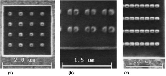
Scanning ion microscope images showing FIB fabricated gold nanopillars on a planar silica substrate: (a) A periodic array of square nanopillars, (b) A periodic array of di-mer nanopillars with a 20 nm gap between the nanopillars forming the di-mer, and (c) Arrays of elliptical gold nanopillars separated by a 15 nm gap
Figure 6.

Scanning ion microscope images showing periodic arrays of FIB fabricated gold nanopillars on the cleaved end-faces of 4-mode optical fibers with the shape of the nanopillars being (a) Circular and (b) Elliptical. (c), (d) Arrays of square nanopillars on the tip of a multimode optical fiber
3.0 Results and Discussion
The results of the FDTD simulations for E-field enhancement factor, i. e. electric field (Ex) in the direction of the long axis of the nanopillars as a ratio of the incident electric field (E0), between two elliptical nanopillars are shown in Figures 1-3. Figures 1b and 1c show the E-field spatial profile around two 130 nm long gold elliptical nanopillars (as ratio of the incident electric field) as the spacing between the nanopillars was varied from 10 nm to 5 nm. This simulation was run at 835 nm with the polarization of the incident electric field along the long axis of the elliptical nanopillars. Figure 2 shows the wavelength dependence of the square of the E-field - in the direction of the long axis of elliptical nanopillars - as a ratio of the square of the incident E-Field. The electric fields shown in Figure 2 are the fields in the center of the gap between the two elliptical-shaped gold nanopillars when the spacing between the two nanopillars was 10 nm. It can be observed from Figure 2 that the highest E-field enhancement was achieved at a wavelength of ~ 835 nm. In order to compare the E-field enhancement values, 835 nm was selected as the wavelength for computing electric fields in the nanopillar gaps for various gap values, viz.5 nm, 10 nm, and 20 nm (Figure 3). One has to remember that the wavelength, at which the maximum in the E-field enhancement occurs, also depends on the spacing between the two 130 nm long elliptical nanopillars. It is noteworthy from Figure 3 that the square of the electric field (Ex) as a ratio of the incident electric field (E0), i. e. (Ex /E0),2 is much higher ~ 4500 when the gap between the two elliptical nanopillars is 5 nm whereas (Ex /E0)2 is ~ 750 and ~ 150 when the gaps are 10 nm and 20 nm, respectively. This feature of increasing enhancement factor with decreasing spacing between the nanostructures underscores the importance of developing nanostructures with less than 10 nm gaps to achieve higher values of E-field enhancement factor. As the value of the SERS signal is proportional to the fourth power of the E-field enhancement factor, a value of (Ex /E0)2 of ~ 4500 in the case of the 5 nm gap implies a SERS EM enhancement factor in the 107 range. As one can observe in Figure 3, the FDTD simulations were run for a simulation time enough for the E-fields to reach a stable value. As an example, it can be seen in Figure 3b that the E-field intensity stabilizes after around 10500 FDTD simulation steps (when cT ~ 6.5 μm, where c is the speed of light and ‘T’ is the time of simulation) out of a total simulation time of 16250 time steps employed in this simulation (cT = 10 μm is the end of the simulation). Hence, the values of E and H fields are evaluated only after 10500 FDTD time steps.
Figure 4 shows three dimensional FDTD calculations of E-fields around two spheroidal nanorods that are separated by gaps between a 2 nm and 20 nm. It can be observed in Figure 4 that there is an increase in the E-field enhancement factor from ~ 8 to 243 when the spacing between the nanorods was decreased from 20 nm to 2 nm. An enhancement factor of 243 implies a SERS EM enhancement factor in the 109range.
Figure 5 shows nanostructures that were fabricated by employing FIB with single or two-step milling processes. The fabrication process of these structures was not time consuming and the fabrication was carried out by employing magnifications of 12 K and 15 K. Figure 5a shows a 4 by 4 array of square nanopillars. Each pillar having a side dimension of approximately 140 nm, was fabricated using a single step milling process. Figure 5b shows an array of di-mer nanopillars with ~ 20 nm gap between the two pillars forming the di-mer whereas Figure 5c shows lines of several gold nanopillars with ~ 15 nm gap between adjacent nanopillars. The structure shown in Figure 5b was developed by using a two-step milling process involving the first step of milling out an array of elliptical nanopillars followed by a second step of milling out the nano-scale gaps (~ 20 nm) between all the nanopillars. The structures shown in Figure 5c were also developed by using a two step milling process involving the first step of milling out several gold nanopillars lines, each line being ~ 4 microns long and 150 nm wide, followed by a second step of milling out several nano-scale gaps (~ 15 nm) on each line. The structures shown in Figures 5b and 5c enable the formation of a high density of regions with narrow gaps between nanostructures, which can translate to SERS ‘hotspots’ or regions where SERS enhancement factor is very high. For finer resolution of nanostructures (i. e. to form smaller gaps between nanostructures) Ga+ ion beams with lower beam diameters would be employed in future work. Figure 6 shows the fabrication of metallic nanopillars on the tips of 4-mode and multimode optical fibers. Developing plasmonic nanostructures, such as nanopillars and nanoholes in metallic films, on the tips of optical fibers provides a convenient macroscopic platform for evaluation of optical properties of these nanostructures. Development of sensors on optical fibers makes these sensors portable, allows remote sensing, decreases electromagnetic interference and creates the ability to embed these sensors in flexible substrates. Figures 6a and 6b show fabrication of circular and elliptical nanopillars, respectively, on the 8 μm diameter core region of the 4-mode optical fiber. In order for the light propagating in the 4-mode optical fiber to interact only with the nanopillars and not the gold film, the gold film was milled out from the core region of the optical fiber tip so as to leave only the nanopillars on the fiber tip. Figures 6c and 6d show a multimode optical fiber with four arrays of nanopillars formed on the 50 μm core region of the optical fiber. It should be noted that FIB provides a convenient process for fabricating metallic nanostructures on the tips of optical fibers so that these fibers could be employed for LSPR or SERS based fiber-optic sensing of chemical and biological molecules.
4. Conclusion
In this work, estimation of E and H fields - in the vicinity of the different metallic nanostructures and in the spacing between the nanostructures - was carried out using Finite Difference Time Domain (FDTD). The different nanostructures investigated were pairs of elliptical nanopillars and spheroidal nanorods with nano-scale gaps (2-20 nm) between the ends of the nanopillars and the nanorods forming the pair. The FDTD calculations provided a direct correlation between the increase in the enhancement factor, i. e. the electromagnetic field as a function of the incident field, of electromagnetic fields in the gap between nanostructures and the decrease in spacing between the nanostructures. In order to fabricate these nanostructures on planar substrates and tips of optical fibers, focused ion beam (FIB) milling was employed. These structures were fabricated on gold-coated planar silica and mica substrates and tips of four mode and multimode optical fibers.
Acknowledgements
This work was sponsored by the U. S. Army Research Office, National Research Council (NRC), and the National Institutes of Health (Grants R01 EB006201 and R01 ES014774).
5.0 References
- [1].Binding, to Protein Immobilized on Gold Nanoparticles by Localized Surface Plasmon Spectroscopy. Anal. Bioanal. Chem. 2006;386:639–644. doi: 10.1007/s00216-006-0559-2. [DOI] [PubMed] [Google Scholar]
- [2].Dhawan A, Gerhold MD, Muth JF. Special Issue of International Journal of High Speed Electronics. 2007. In-line fiber sensors for environmental sensing. In press. [Google Scholar]
- [3].Dhawan A, Muth JF. In-line optical fiber sensors for environmental sensing applications. Optics Lett. 2006;31:1391–1393. doi: 10.1364/ol.31.001391. [DOI] [PubMed] [Google Scholar]
- [4].Gerhold M,D, Dhawan A, Muth J,F. In-line fiber sensors for environmental sensing. Proc. Intl. Sym. For Spectral Sensing Research. 2006 [Google Scholar]
- [5].Vo-Dinh T, Hiromoto MYK, Begun GM, Moody RL. Surface-Enhanced Raman Spectroscopy for Trace Organic Analysis. Anal. Chem. 1984;56:1667. [Google Scholar]
- [6].Alak AM, Vo-Dinh T. Surface-Enhanced Raman Spectrometry of Organo-Phosphorus Chemical Agents. Anal. Chem. 1987;59:2149. doi: 10.1021/ac00144a030. [DOI] [PubMed] [Google Scholar]
- [7].Nie S, Emory SR. Probing single molecules and single nanoparticles by surface-enhanced Raman scattering. Science. 1997;275:1102–1106. doi: 10.1126/science.275.5303.1102. [DOI] [PubMed] [Google Scholar]
- [8].Kneipp K, Wang Y, Keipp H, Perelman LT, Itzkan I, Dasari RR, Feld MS. Single molecule detection using surface-enhanced Raman scattering (SERS) Phys. Rev. Lett. 1997;78:1667–1670. [Google Scholar]
- [9].Haes AJ, Van Duyne RP. A unified view of propagating and localized surface plasmon resonance Biosensors. Anal. Bioanal. Chem. 2004;379:920–930. doi: 10.1007/s00216-004-2708-9. [DOI] [PubMed] [Google Scholar]
- [10].Dhawan A, Muth JF. Plasmon resonances of gold nanoparticles incorporated inside an optical fibre matrix. Nanotechnology. 2006;17:2504–2511. doi: 10.1088/0957-4484/17/10/011. [DOI] [PubMed] [Google Scholar]
- [11].Raether H. Surface plasmons on smooth and rough surfaces and on gratings. Springer Verlag; Berlin: 1988. [Google Scholar]
- [12].Fujiwara K, Watarai H, Toh H, Nakahama E, Ogawa N. Measurement of Antibody Binding, to Protein Immobilized on Gold Nanoparticles by Localized Surface Plasmon Spectroscopy. Anal. Bioanal. Chem. 2006;386:639–644. doi: 10.1007/s00216-006-0559-2. [DOI] [PubMed] [Google Scholar]
- [13].Le Ru EC, Etchegoin PG, Meyer M. Enhancement factor distribution around a single surface-enhanced Raman scattering hot spot and its relation to single molecule detection. Journal of Chemical Physics. 2006;125:204701. doi: 10.1063/1.2390694. [DOI] [PubMed] [Google Scholar]
- [14].Maxwell DJ, Emory SR, Nie S. Nanostructured thin-film materials with surface-enhanced optical properties. Chem. Mater. 2001;13:1082–1088. [Google Scholar]
- [15].Otto A, Mrozek I, Grabhorn H, Akemann W. Surface-enhanced Raman scattering. J. Phys.: Condens. Matter. 1992;4:1143–1212. [Google Scholar]
- [16].Vo-Dinh T. Surface-Enhanced Raman Spectroscopy Using Metallic Nanostructures. Trends in Anal. Chem. 1998;17:557–582. [Google Scholar]
- [17].Vo-Dinh T. SERS Chemical Sensors and Biosensors: New Tools for Environmental and Biological Analysis. Sensors and Actuators. 1995;29:183–189. [Google Scholar]
- [18].Taflove A, Hagness S,C. Computational Electrodynamics: The Finite-Difference Time-Domain Method. 2nd ed. Artech; Boston, MA: 2000. [Google Scholar]
- [19].Lazzi G, Gandhi O,P. Realistically tilted and truncated anatomically based models of the human head for dosimetry of mobile telephones. IEEE Trans. Electromagn. Compat. 1997;39:55–61. [Google Scholar]
- [20].Futamata M, Maruyama Y, Ishikawa M. Local Electric Field and Scattering Cross Section of Ag Nanoparticles under Surface Plasmon Resonance by Finite Difference Time Domain Method. J. Phys. Chem. B. 2003;107(31):7607–7617. [Google Scholar]
- [21].Phillips, Griffis DP, Russell PE. Channeling effects during focused-ion-beam micromachining of copper. Journal of Vacuum Science & Technology A. 2000;18:1061. [Google Scholar]
- [22].Gonzalez JC, Griffis DP, Miau TT, Russell PE. Chemically enhanced focused ion beam micromachining of copper. Journal of Vacuum Science & Technology B: Microelectronics and Nanometer Structures. 2001;19(6):2539–2542. [Google Scholar]
- [23].Tseng A,A. Recent developments in nanofabrication using focused ion beams. Small. 2005;1(10):924–939. doi: 10.1002/smll.200500113. [DOI] [PubMed] [Google Scholar]