Abstract
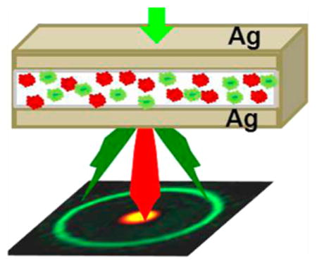
Controlling the emission properties of fluorophores is essential for improving the performance of fluorescence-based techniques in modern biochemical research, medical diagnosis, and sensing. Fluorescence emission is isotropic in nature, which makes it difficult to capture more than a small fraction of the total emission. Metal– dielectric–metal (MDM) substrates, discussed in this Letter, convert isotropic fluorescence into beaming emission normal to the substrate. This improves fluorescence collection efficiency and also opens up new avenues for a wide range of fluorescence-based applications. We suggest that MDM substrates can be readily adapted for multiple uses, such as in microarray formats, for directional fluorescence studies of multiple probes or for molecule-specific sensing with a high degree of spatial control over the fluorescence emission.
SECTION: Physical Processes in Nanomaterials and Nanostructures
Fluorescence detection has become a dominant technology in the biosciences. Until recently, almost all efforts to modify molecular fluorescence have been based on modification of the chemical structure of the fluorophore. In recent years, this laboratory and others have focused on the modification of fluorescence spectral properties using nearby metallic structures.1–8 These efforts represent a fundamental shift from using the intrinsic far-field emission from fluorophores to using near-field interaction, for modifying the quantum yields, anisotropy, and directionality of the emission. These effects depend on collective oscillation of electrons in metals, which are called surface plasmons. The optical fields near fluorophores can couple to the surface plasmon oscillations of metallic substrates as localized excitations for metal nanoparticles or as propagating surface waves for thin metal films. This offers exciting new opportunities for directing and controlling the flow of optical energy using near-field effects rather than classical far-field optical components.5–7 Over the past several years, we observed that emission from fluorophores located near thin metal films on a glass substrate enters the substrate at an angle defined by the surface plasmon resonance (SPR) angle for the emission wavelength.1,2 This phenomenon of surface-plasmon-coupled emission (SPCE) has several remarkable features that can complement and improve fluorescence technology.9,10 One of the advantages of SPCE is that it directs the fluorescence emission in a sharply defined angle, leading to a narrow cone of emission. This is very useful because fluorescence emission is isotropic in nature, which makes it difficult to detect more than a small fraction of the total emission. With SPCE, most of the emission can be captured by a detector, leading to significant improvements in the fluorescence collection efficiency.1,2 However, SPCE typically occurs at a large angle from the surface normal axis which is a disadvantage in multiplexing or array-type applications. It would certainly be more advantageous if we could obtain the fluorescence emission as a single, highly collimated beam with greater control over the emission directionality.
In this Letter, we demonstrate that the emission from randomly oriented fluorophores can be converted into narrow emission beaming normal to the surface, with planar metal–dielectric–metal (MDM) substrates. Importantly, our MDM structures can be made with simple vapor deposition methods without the need for top-down nanofabrication of features in the substrate plane. The MDM structures can support both photonic as well as plasmonic modes that can act together under suitable conditions. We show that these structures can be easily adapted for controlling the direction of emission as well as other fluorescence properties, like the emission spectra and lifetimes of fluorophores embedded within the dielectric medium of the substrate. The beaming emission not only improves the fluorescence collection efficiency but also provides the opportunity for a wide range of fluorescence based applications. We suggest that MDM substrates can be integrated in lab-on-chip formats to monitor different kinds of interactions in a single frame with microarray technology. They can be incorporated in a regular microscope for fluorescence imaging or single-molecule studies. They can also be used for directional fluorescence studies of multiple probes or for molecule-specific sensing, with a high degree of spatial control.
The MDM substrates in the present study were prepared by thermal vapor deposition of 50 nm Ag films on cleaned glass slides, followed by spin coating an aqueous solution of poly(vinyl alcohol) (PVA) containing the dyes. The dielectric thicknesses on the substrates were varied from ∼120 to 400 nm by using different weight percentages of PVA (see Supporting Information, Figure S1). A layer of 50 nm Ag was then vapor-deposited above the PVA layer to obtain the final substrates. The MDM samples were illuminated in the reverse Kretschmann (RK) configuration, which in this case is the incident light impinging on the top Ag surface. The fluorescence was collected using an optical fiber (Scheme 1).
Scheme 1. Illumination Geometry (Reverse Kretschmann, RK) and Angle Notations Used in the Studya.
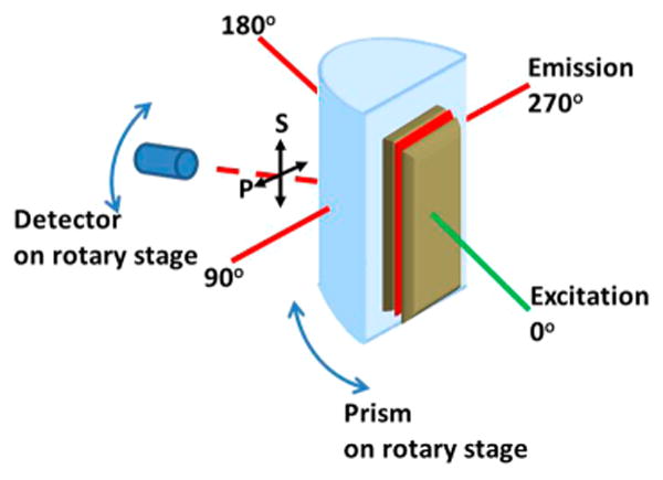
aAg-PVA-Ag substrate is prepared on a glass slide and fixed to the prism with glycerol. The s- and p-polarizations are shown for clarity
Both the detector and the sample were placed on a rotation stage to enable excitation and detection at different angles. Further details of the experimental setup and the illumination geometry are provided in the Supporting Information.
Figure 1 shows the variation in the angular distribution of emission from sulforhodamine101 (S101) embedded in dielectric PVA layers of different thicknesses between 50 nm thick Ag films (Ag-PVA-Ag, MDM substrates). Interestingly, no emission is observed for the samples with <4% PVA concentration. At 4% PVA concentration, which corresponds to a film thickness of ∼150 nm, the emission is highly directional and is mostly concentrated in a narrow beam normal to the substrate, with a half angle spread of ∼18° from the normal. With increasing PVA concentrations, the emission pattern gradually changes, with the s- and p-polarized components appearing at definite angles. At 8% PVA concentration, beaming emission is observed again but is also accompanied by an s-polarized component at a different angle.
Figure 1.
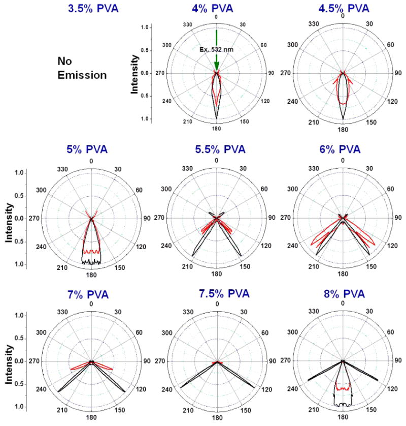
Angular distributions of the fluorescence intensities for s- (black) and p-polarized (red) emission of S101 embedded in Ag-PVA-Ag substrates with different PVA concentrations. The calibration curve for the PVA film thickness obtained with varying PVA concentrations is provided in the Supporting Information.
Metallo-dielectric layered structures are currently being investigated for applications like waveguides for photon transport, tunable color filters, and electro-optic devices.11–13 To the best of our knowledge, this is the first observation of beaming emission normal to the surface using planar MDM substrates, without nanoscale lateral features. Recently, plasmonic beaming of fluorescence has been studied with optical antennas consisting of circular gratings and nano-holes.3,4 This approach was confined to a small area and involved complex and expensive nanofabrication. In this context, the observation of beaming emission with simple, large-area Ag-PVA(4%)-Ag substrate, is quite exciting. The significance of this observation is further strengthened by the fact that the emission pattern is unaffected by the direction of excitation. Similar beaming emission is observed even when the excitation angle is changed to 40° instead of the normal excitation at 0° (see Supporting Information, Figure S2).
On the basis of our previous studies on SPCE, it is now understood that SPCE is related to SPR, a technique widely used for bioaffinity studies. In brief, the SPCE phenomenon arises due to the near-field interaction of excited fluorophores with the metal film. Near-fields around fluorophores have large wave vectors and are thus able to create surface plasmons in the metal film. The surface plasmons in turn radiate into the substrate at definite angles and with interesting polarization properties. An intuitive understanding of SPCE can be obtained from the principles of SPR. In SPR, a thin metal film is illuminated through a prism (Kretschmann, KR configuration). The film is highly reflective, except at a particular angle called the SPR angle. At this angle, the film absorbs incident light due to the creation of surface plasmons in the metal. The emission patterns for SPCE satisfy the same conditions required for observing the minimum reflectivity from the substrates in SPR.1,2,9,10,14,15 We anticipated that this should also be the case for the present MDM substrates. Figure 2 shows the reflectivity curves calculated using the software package, TF Calc, for S101 emission (600 nm) in the Ag-PVA(4%)-Ag and Ag-PVA(8%)-Ag substrates. Indeed, the calculated angle-dependent reflectivity curves are found to be in close agreement with the angular emission patterns of S101 observed with these substrates. More specifically, at 150 nm PVA thickness, the reflectivity is at a minimum for light normal to the surface, which corresponds to the normal emission for 4% PVA shown in Figure 1. Similarly, for 350 nm PVA thickness, there is a reflectivity minimum for light normal to the surface along with s-polarized reflectivity minima at the corresponding emission angles (∼120 and 240°) observed for 8% PVA, as shown in Figure 1.
Figure 2.
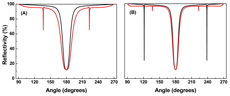
Calculated reflectivity curves for 600 nm s- (black) and p-polarized (red) light for (A) Ag-PVA(4%)-Ag, PVA thickness 150 nm and (B) Ag-PVA(8%)-Ag, PVA thickness 350 nm.
It is also useful to compare the emission pattern of the Ag-PVA-Ag, MDM substrate with that observed for a substrate consisting of S101 in 4% PVA above a single 50 nm Ag film (PVA(4%)-Ag). In the latter case, the emission is strictly s-polarized and is observed at an angle of ∼135° (and ∼225° due to symmetry), leading to a cone of emission, with no emission normal to the surface (see Supporting Information, Figure S3). This is in accordance with our previous studies on SPCE and waveguide effects in thick dielectric films.1,2Figure 3 shows the emission spectra of S101 in the Ag-PVA-Ag, MDM substrate and in PVA-Ag. It is interesting to note that the SPCE spectra of S101 in the PVA(4%)-Ag sample shows considerable wavelength dispersion, and the emission appears to be different at the various observation angles. The emission spectra of S101 in the Ag-PVA(4%)-Ag substrate remain unchanged at different observation angles but are narrower toward the red edge. The dispersion effect in the PVA(4%)-Ag sample can be explained by considering the broad emission bandwidth of S101 and the condition that each wavelength in the spectrum couples to the propagating surface plasmons in the metal–dielectric interface only at a defined angle. So, although the emission appears different at different observation angles, the overall SPCE emission spectra obtained by summation of all individual spectra matches with the free space emission of S101 (see Supporting Information, Figure S4). To understand the lack of dispersion and narrowing in the spectra of S101 in Ag-PVA(4%)-Ag, we have to consider the interference effect of light in multilayer structures.
Figure 3.
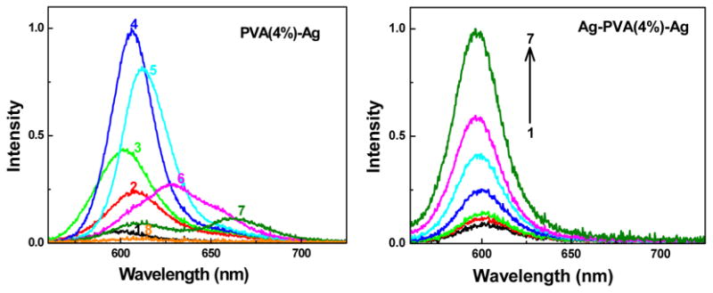
Emission spectra of S101 (s-polarized) from the PVA(4%)-Ag substrate recorded at 125, 130, 132, 133, 134, 135, 136, and 140° (1–8) and the Ag-PVA(4%)-Ag substrate recorded at 125, 130, 140, 150, 160, 170, and 180° (1–7).
The Ag-PVA-Ag, MDM structures can be considered to be a planar microcavity consisting of two metallic mirrors separated by a dielectric film, thus forming a Fabry–Perot resonator. Accordingly, the emission properties of a fluorophore embedded within this microcavity will be affected by the geometry of the substrate. The resonant modes of this microcavity will be at wavelengths (λresonance) where the following conditions are satisfied:
| (1) |
Here m is an integer, n is the refractive index of PVA (n = 1.52), and deffective is the effective cavity thickness. The effective thickness comprises dPVA, the distance between the Ag films determined by the physical thickness of the PVA layer, and dphase-change that arises due to the phase change on reflection at the Ag films.16,17 The first resonance condition (m = 1) for the emission wavelength of 600 nm (corresponding to the emission maximum of S101) should be satisfied at an effective thickness (deffective) of 300 nm. For ideal reflecting mirrors, the phase change on reflection is π, and in this case deffective = ndPVA, so the resonance condition would be observed at a PVA thickness of ∼197 nm. Because the beaming emission is observed for the Ag-PVA(4%)-Ag substrate with PVA thickness (dPVA) of 150 nm that is less than the ideal case, it implies that the phase change due to reflection from the two Ag surfaces in the MDM substrate contributes toward the effective thickness (dphase-change). Below a dielectric thickness of 150 nm, no resonant mode exists for the present Ag-PVA-Ag substrates and hence no emission is observed from S101 for PVA concentrations less than 4% (Figure 1). Furthermore, a dielectric thickness of 150 nm cannot support modes with higher wavelengths. This explains the narrowing in the red-edge of the emission spectra of S101 in the Ag-PVA(4%)-Ag substrate. The second Fabry–Perot resonance mode for the Ag-PVA-Ag substrate appears at a dielectric thickness of 350 nm and matches well with the beaming emission observed in the Ag-PVA(8%)-Ag sample. From the above discussion, it can be easily understood that the emission angle of a fluorophore can be tailored in a relatively straightforward manner by changing the thickness or type of the dielectric layer or by altering the phase changes on reflection at the metallic surfaces. This can be possible either by changing the thickness of the Ag film or even using other metals such as Au or Al depending on the emission wavelength.
Considering that the MDM substrate corresponds to a planar microcavity, it is expected that the spontaneous emission rate for a fluorophore placed within the microcavity will be increased due to the alteration in the photonic mode density (Purcell effect).18,19 A significant reduction in the fluorescence lifetime of S101 is in fact observed in the Ag-PVA(4%)-Ag substrate (average lifetime ∼3 ns) in comparison with the lifetime of S101 (∼4 ns) in PVA(4%) spin-coated on glass (see Supporting Information, Figure S5). This is a favorable result because a fluorophore that spends less time in the excited state can undergo more excitation emission cycles prior to photodecomposition. Hence, a reduction in the fluorescence lifetime should lead to increased photostability of the fluorophore. The intensity decay is multi- or non-exponential in the MDM substrate. This suggests that the fluorophore– plasmon coupling depends on the location of the fluorophore on the dielectric, the orientation of the emission dipole relative to the planar metal surface, or both.
To examine further the emission directionality of the MDM substrate, we have studied the emission patterns for another fluorophore, Cy5, that is widely used for biochemical studies. For Cy5 (having emission maximum ∼670 nm), the beaming emission is observed with the Ag-PVA(6%)-Ag substrate, which corresponds to a dielectric thickness of ∼175 nm (see Supporting Information, Figure S6). In this case, the half angle spread of the beaming emission is ∼15° from the normal. It may be recollected that at ∼175 nm dielectric thickness, the emission from S101 is observed at different angles depending on polarization. This result has enormous significance because the emission directionality also carries information about the nature of the fluorophore. In other words, the Ag-PVA-Ag, MDM substrates can be used for multicolor directional fluorescence sensing of multiple probes. This is demonstrated more clearly by recording the angular distribution of emission for a mixture of S101 and Cy5 in the Ag-PVA(6%)-Ag substrate (Figure 4). The emission from Cy5 is observed as a narrow beam normal to the substrate, whereas the emission from S101 is observed at ∼145°. Accordingly, the emission spectrum recorded at 180° shows the usual Cy5 spectral features, whereas the emission spectral features of S101 are clearly evident at 145°. It is important to mention that the changes in the angular dependence of the emission intensities with change in the emission wavelengths is more pronounced for the present MDM substrates in comparison with the usual SPCE substrates with a single metal layer.1
Figure 4.
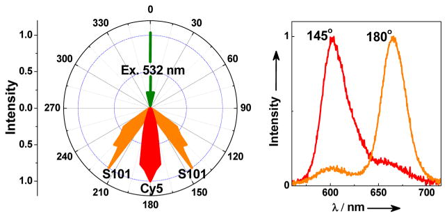
Angular distribution for emission at 600 nm (S101) and 670 nm (Cy5) for a mixed sample of S101 and Cy5 in Ag-PVA(6%)-Ag. Right panel shows emission spectra recorded for the mixed sample at 145 and 180° observation angles.
The observation of beaming emission from the MDM substrates opens up a broad subject area, and numerous fluorescence-based applications can be envisaged. Figure 5 shows a schematic representation and real color photographs of the images formed by projecting the emission from S101 embedded in the Ag-PVA-Ag and PVA-Ag substrates on a screen. The PVA-Ag substrate generates a ring of fluorescence for each excitation spot, whereas the PVA-Ag substrate generates a ring of fluorescence for each excitation spot, the Ag-PVA-Ag substrate shows distinct fluorescence spots corresponding to each excitation. This Figure thus serves to demonstrate the ease with which the present MDM substrates can be adapted for fluorescence studies in microarray formats (also see Supporting Information, Figure S7). Fluorescence microarray technology is a powerful tool for high throughput bioanalytical studies due to its miniaturization, low material consumption, ability for multiplexing, and automation.20 We believe that the high spatial control and beaming emission from the MDM substrates will permit focusing onto an imaging detector with simple and inexpensive optics and will reduce crosstalk between adjacent spots, thus improving data quality.
Figure 5.
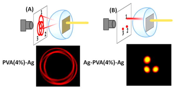
Illumination scheme and superimposed photographs of the fluorescence images of S101 projected on a screen for each excitation spot in (A) PVA-Ag and (B) Ag-PVA-Ag.
One limitation of the MDM substrates is that the fluorophores are embedded within the dielectric between the Ag layers and are not amenable for dynamic studies or binding interactions. For bioanalytical applications it is important to be able to access the analyte surface so that chemistry can be performed. Recently, there have been studies of energy transfer (ET) across a metal film mediated by surface plasmon polaritons (SPPs).21,22 The mechanism of SPP-ET is different from conventional nonradiative Forster ET and involves the coupling of donor emission to the surface plasmon modes of the first metal–dielectric interface, followed by cross coupling of the SPPs on opposite sides of the metal film and ET to the acceptor molecules on the second metal–dielectric interface. These concepts can be utilized in the present MDM substrates for bioassays or bioanalytical applications. A schematic representation of SPP-ET with the MDM substrates is presented in Figure 6. The topmost Ag layer can be coated with biomarkers capable of attaching to specific fluorescence donor labeled biomolecules. The dielectric layer between the metals can contain the fluorescence acceptor. Under suitable binding conditions, SPP-ET will lead to the observation of directional emission from the embedded acceptor molecules. This configuration will thus allow molecule-specific biosensing, with the advantage of a high degree of spatial control over the fluorescence emission. To demonstrate the feasibility of this concept, we have studied the SPP-ET from the donor, tris-(8-hydrxyquinoline)aluminum (AlQ3) spin coated on the top Ag layer, to the acceptor, rhodamine6G (Rh6G) embedded inside the substrate. In these substrates, the donor, AlQ3, is spin coated above the top Ag layer using a poly(methyl methacrylate) (PMMA) solution in chloroform. An increase in the fluorescence intensity of Rh6G accompanied by a decrease in the fluorescence intensity of AlQ3 is observed for the donor–acceptor samples. This suggests the occurrence of SPP-ET from AlQ3 to Rh6G. A quantitative estimate of the SPP-ET efficiency (FET) can be determined from the area under the donor–acceptor (IDA) and acceptor only (ID) curves, as FET ≈ (IDA – IA)/IDA. 21,22 For the present MDM substrates, the fraction of the total donor–acceptor sample emission attributable to SPP-ET is estimated to be ∼0.35. A more rigorous test for the ET process is to examine the intensity decays of the donor and acceptor samples. A long lifetime component, corresponding to that of AlQ3, is observed for Rh6G in the presence of the donor, which confirms SPP-ET from AlQ3 to Rh6G (see Supporting Information, Table S1).
Figure 6.
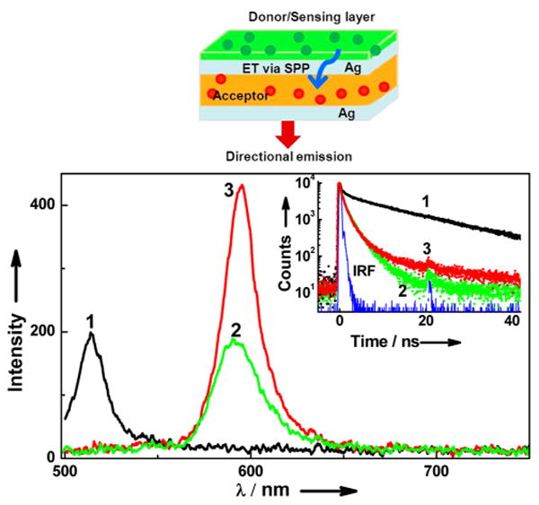
Fluorescence spectra and intensity decays (inset) for (1) donor only, AlQ3/PMMA(4%)-Ag-PVA(4%)-Ag, (2) acceptor only, PMMA(4%)-Ag-PVA(4%)/Rh6G-Ag, and (3) donor–acceptor, AlQ3/ PMMA(4%)-Ag-PVA(4%)/Rh6G-Ag samples with 470 nm excitation and observed at 180°. Top panel shows schematic of the SPP-ET process.
In summary, the present study demonstrates that MDM substrates can channel the fluorescence into a narrow beam and allow greater control over the emission directionality, which is highly desirable for improved fluorescence detection. These structures also allow us to modify the fluorescence lifetimes and polarization of the emission. Importantly, the MDM substrates can be easily and reproducibly fabricated using standard thermal evaporation techniques. So, the fluorescence from different dyes can be conveniently tuned to suit our needs by changing the nature and thickness of the metal or the dielectric medium. The MDM substrates are promising for both fundamental light matter interactions and device applications. We believe that many novel fluorescence based studies can be designed with the present MDM plasmonic substrates.
Supplementary Material
Acknowledgments
We thank the UMCP Fablab for Profilometer use. This work was supported by NIH Grants HG002655, EB006521 (J.R.L.) and AI087968 (K.R.). S.D.C. acknowledges the Indo-US Science and Technology Forum (IUSSTF) for the IUSSTF Fellowship.
Footnotes
Notes: The authors declare no competing financial interest.
Supporting Information: Figures S1-S7, Table S1, substrate preparation, experimental setups, and methods. This material is available free of charge via the Internet at http://pubs.acs.org
References
- 1.Gryczynski I, Malicka J, Gryczynski Z, Lakowicz JR. Radiative Decay Engineering 4. Experimental Studies of Surface Plasmon-Coupled Directional Emission. Anal Biochem. 2004;324:170–182. doi: 10.1016/j.ab.2003.09.036. [DOI] [PMC free article] [PubMed] [Google Scholar]
- 2.Gryczynski I, Malicka J, Nowaczyk K, Gryczynski Z, Lakowicz JR. Effects of Sample Thickness on the Optical Properties of Surface Plasmon-Coupled Emission. J. Phys Chem B. 2004;108:12073–12083. doi: 10.1021/jp0312619. [DOI] [PMC free article] [PubMed] [Google Scholar]
- 3.Jun YC, Huang KCY, Brongersma ML. Plasmonic Beaming and Active Control Over Fluorescent Emission. Nat Commun. 2011;283:1–6. doi: 10.1038/ncomms1286. [DOI] [PubMed] [Google Scholar]
- 4.Aouani H, Mahboub O, Devaux E, Rigneault H, Ebbesen TW, Wenger J. Plasmonic Antennas for Directional Sorting of Fluorescence Emission. Nano Lett. 2011;11:2400–2406. doi: 10.1021/nl200772d. [DOI] [PubMed] [Google Scholar]
- 5.Schuller JA, Barnard ES, Cai W, Jun YC, White JS, Brongersma ML. Plasmonics for Extreme Light Concentration and Manipulation. Nat Mater. 2010;9:193–204. doi: 10.1038/nmat2630. [DOI] [PubMed] [Google Scholar]
- 6.Lal S, Link S, Halas NJ. Nano-Optics from Sensing to Waveguiding. Nat Photonics. 2007;1:641–648. [Google Scholar]
- 7.Barnes WL, Dereux A, Ebbesen TW. Surface Plasmon Subwavelength Optics. Nature. 2003;424:824–830. doi: 10.1038/nature01937. [DOI] [PubMed] [Google Scholar]
- 8.Curto AG, Volpe G, Taminiau TH, Kreuzer MP, Quidant R, van Hulst NF. Unidirectional Emission of a Quantum Dot Coupled to a Nanoantenna. Science. 2010;329:930–932. doi: 10.1126/science.1191922. [DOI] [PubMed] [Google Scholar]
- 9.Yuk JS, McDonagh C, MacCraith BD. Demonstration of a Surface Plasmon-Coupled Emission (SPCE)-Based Immunoassay in the Absence of a Spacer Layer. Anal Bioanal Chem. 2010;398:1947–1954. doi: 10.1007/s00216-010-4026-8. [DOI] [PubMed] [Google Scholar]
- 10.Xie TT, Liu Q, Cai WP, Chen Z, Li YQ. Surface Plasmon-Coupled Directional Emission Based on a Conformational-Switching Signaling Aptamer. Chem Commun. 2009:3190–3192. doi: 10.1039/b823352g. [DOI] [PubMed] [Google Scholar]
- 11.Chandran A, Barnard ES, White JS, Brongersma ML. Metal-Dielectric-Metal Surface Plasmon-Polariton Resonators. Phys Rev B. 2012;85:085416. [Google Scholar]
- 12.Diest K, Dionne JA, Spain M, Atwater HA. Tunable Color Filters Based on Metal-Insulator-Metal Resonators. Nano Lett. 2009;9:2579–2583. doi: 10.1021/nl900755b. [DOI] [PubMed] [Google Scholar]
- 13.Dionne JA, Lezec HJ, Atwater HA. Highly Confined Photon Transport in Subwavelength Metallic Slot Waveguides. Nano Lett. 2006;6:1928–1932. doi: 10.1021/nl0610477. [DOI] [PubMed] [Google Scholar]
- 14.Enderlein J, Ruckstuhl T. The Efficiency of Surface-Plasmon Coupled Emission for Sensitive Fluorescence Detection. Opt Express. 2005;13:8855–8865. doi: 10.1364/opex.13.008855. [DOI] [PubMed] [Google Scholar]
- 15.Calander N. Surface Plasmon-Coupled Emission and Fabry-Perot Resonance in the Sample Layer: A Theoretical Approach. J Phys Chem B. 2005;109:13957–13963. doi: 10.1021/jp0510544. [DOI] [PubMed] [Google Scholar]
- 16.Becker H, Burns SE, Tessler N, Friend RH. Role of Optical Properties of Metallic Mirrors in Microcavity Structures. J Appl Phys. 1997;81:2825–2829. [Google Scholar]
- 17.Becker H, Friend RH, Wilkinson TD. Light Emission from Wavelength-Tunable Microcavities. Appl Phys Lett. 1998;72:1266–1268. [Google Scholar]
- 18.Purcell EM. Spontaneous Emission Probabilities at Radio Frequencies. Phys Rev. 1946;69:681. [Google Scholar]
- 19.Worthing PT, Barnes WL. Spontaneous Emission within Metal-Clad Microcavities. J Opt A: Pure Appl Opt. 1999;1:501–506. [Google Scholar]
- 20.Nagl S, Schaeferling M, Wolfbeis OS. Fluorescence Analysis in Microarray Technology. Microchim Acta. 2005;151:1–21. [Google Scholar]
- 21.Andrew P, Barnes WL. Energy Transfer across a Metal Film Mediated by Surface Plasmon Polaritons. Science. 2004;306:1002–1005. doi: 10.1126/science.1102992. [DOI] [PubMed] [Google Scholar]
- 22.Collini E, Todescato F, Ferrante C, Bozio R, Scholes GD. Photophysics and Dynamics of Surface Plasmon Polaritons-Mediated Energy Transfer in the Presence of an Applied Electric Field. J Am Chem Soc. 2012;134:10061–10070. doi: 10.1021/ja3014314. [DOI] [PubMed] [Google Scholar]
Associated Data
This section collects any data citations, data availability statements, or supplementary materials included in this article.


