Abstract
A hybrid structure (HS) made of one-dimensional ZnO nanorods (NRs) and a two-dimensional synthesized graphene sheet was successfully constructed in this study. The uniform ZnO NRs were obtained by hydrothermal method and grown on a graphene surface that had been transferred to a polyethylene terephthalate substrate. The HS exhibited high transmittance (approximately 75%) over the visible wavelength range, even after cyclic bending with a small radius of curvature. Raman spectroscopy and Hall measurement were carried out to verify the chemical composition and electrical properties of the structure. Stable electrical conductance of the ZnO NR/graphene HS was achieved, and increase in carrier mobility decreased the resistance of the ZnO-with-graphene sheet in comparison with bare ZnO NRs.
Keywords: Hybrid structure, ZnO nanorods, Graphene sheet, Transmittance, Hall measurement
Background
Various investigations have concentrated on the development of promising materials with multifunctionality for emerging electronic and optoelectronic systems [1,2]. For example, interest has been growing in combining the specific properties of different dimensional structures on a flexible and transparent substrate. Recently, the composition of hybrid structures (HS) using one-dimensional (1D) and two-dimensional (2D) components to synthesize novel materials has been gaining much attention, especially for 1D ZnO nanorods (NRs) and 2D graphene sheets. Graphene, which consists of monolayers of sp2 hybrid carbon atoms, has been the most attractive carbon material in recent years [3-6]. Because of carbon-carbon covalent bonds, a graphene sheet exhibits extraordinary electrical and mechanical properties, including high intrinsic mobility (15,000~20,000 cm2/Vs) [7], a stretchable nature, and high thermal conductivity (approximately 5,300 W/mK) [8]. Moreover, with high optical transmittance and high chemical stability, graphene is a promising building block of window material for optoelectronic devices. In addition to graphene, transparent ZnO NRs with a wide bandgap are good candidates for use in next-generation electronics and optoelectronics [9-13]. Many methods have been developed to prepare ZnO NRs, including chemical vapor deposition (CVD) [14], vapor–liquid-solid epitaxy [15], and pulsed laser deposition [16]. However, these techniques are only applicable to limited substrate sizes and require high process temperatures, which are prohibitive for many practical applications. On the other hand, the hydrothermal process is regarded as a promising technique for the synthesis of ZnO NRs because it has several advantages, including the fact that it is a low-cost and low-temperature process that provides wafer-scale uniformity and high growth rates. Therefore, the hybridization of 2D graphene with 1D ZnO NRs has recently been reported for multifunctional applications, such as gas sensors [17], light-emitting diodes [18], solar cells [19], and piezoelectric nanogenerators [20]. In addition, ZnO is an excitingly attractive material for use as a transparent conducting oxide (TCO), but ZnO cannot solitarily exist as a TCO because of its intrinsic point defects [21,22]. To overcome this problem, increasing the carrier concentration or carrier mobility is effectively equivalent to decreasing the sheet resistance. In our opinion, ZnO NR/graphene HSs have characteristics that are of particular interest to the development of such structures for use as TCOs.
In this work, 1D ZnO NRs were synthesized by hydrothermal method onto a 2D graphene sheet to form an HS. High transmittance over the visible light region was obtained after synthesizing the ZnO NRs, and the sample displayed excellent mechanical properties after bending with a small radius. Notably, we essayed a Hall measurement of the HS, which consisted of ZnO NRs/graphene on a polyethylene terephthalate (PET) substrate.
Methods
Each graphene sheet was prepared on a Cu foil by CVD and then spin-coated with a protective layer of poly(methyl methacrylate) (PMMA). The PMMA/graphene/Cu foil sample was immersed into an FeCl3/HCl solution for etching to strip the Cu foil. After etching, we retrieved the sample from the FeCl3/HCl solution, transferred it onto the PET substrate, and cleaned it with deionized water. Finally, the PMMA/graphene was soaked in an acetone solution to remove the PMMA and then washed with isopropyl alcohol [23]. A 100-nm ZnO seed layer was coated onto the graphene sheet with an E-gun evaporation system. Following this step, the ZnO NRs were grown in an equal molar aqueous solution of hexamethylenetetramine (HMTA) and zinc nitrate hexahydrate at 95°C for 2 h. The sample was cleaned with acetone and deionized water and then dried at room temperature. After the growth process, a morphological study of the ZnO nanostructures was performed with a JEOL JSM-6500 (Tokyo, Japan) field-emission scanning electron microscope (FE-SEM). Optical transmittance measurements were collected for nearly normal light incidence covering the spectral region from 400 to 800 nm with a standard UV-Visible spectrometer (ARN-733, JASCO, Easton, MD, USA). In this measurement, the noise level was approximately 0.002%. Raman spectrum was measured with a triple spectrometer (T64000, HORIBA Jobin Yvon SAS, Canal, France) equipped with a charge-coupled device cooled to 160 K. Hall measurement was performed with an Ecopia Hall effect measurement system (HMS-3000 ver 3.51.4).
Results and discussion
To investigate the 3D hybrid nanostructure formed by combining 1D ZnO NRs with2D graphene, the ZnO seed layer was coated onto the graphene surface and annealed at a suitable temperature for the growth of ZnO NRs through hydrothermal method. The ZnO NRs presented here were obtained with a solution-based chemical synthesis. In a solution containing zinc nitrate hexahydrate and HMTA, hydroxyl ions were released through the thermal decomposition of the HMTA and reacted with zinc ions to form ZnO. The synthesis can be summarized in the following reactions:
| (1) |
| (2) |
| (3) |
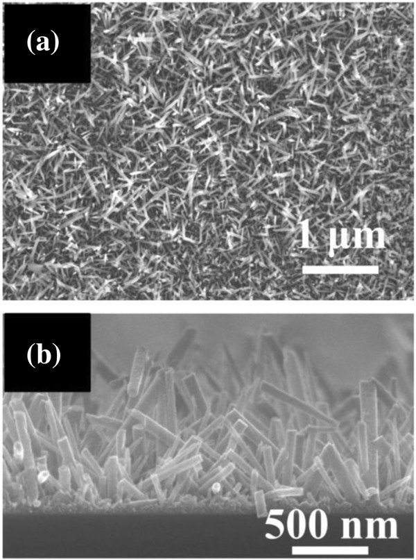
To observe the growth of the ZnO NRs on the graphene sheet, FE-SEM images were taken, as shown in Figure 1. Uniform ZnO NRs were successfully grown on the graphene surface. The average length and diameter of the NRs were 1 μm and 75 nm, respectively. The favored [0001] orientation of the ZnO NRs can be explained by the intrinsic high energy of the O2− terminated surface, onto which the precursor molecules in the vicinity tend to be adsorbed [24]. Simultaneously, the HMTA supplies the solution with hydroxide ions, and Zn2+ cations usually form hydroxyl complexes as the precursors of ZnO.
Figure 1.
Plane-view (a) and cross-sectional (b) FE-SEM micrographs of ZnO NRs grown on graphene.
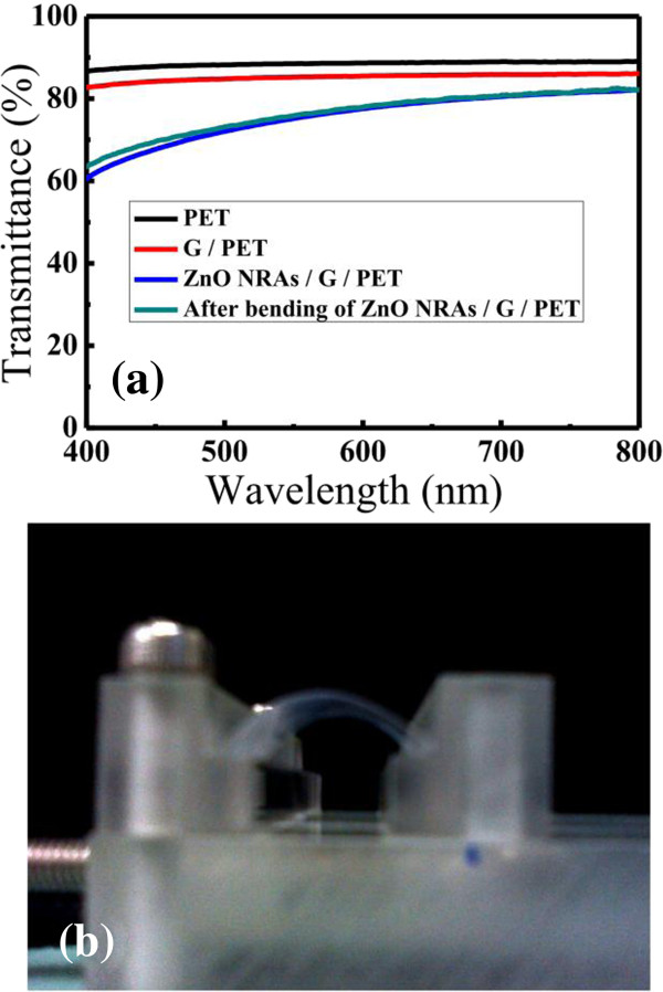
A concerning feature of the hybrid structure is that, although ZnO and graphene exhibit good optical transmittance in the visible spectral range, the scattering of light by ZnO NRs is suspected to lead to a decrease in transmittance to a certain extent. The optical transmittance of the ZnO NR/graphene hybrid structure was estimated by fabricating the structures on PET substrates. Figure 2a shows the optical transparency of PET, graphene/PET, and ZnO NRs/graphene/PET before and after bending. The average transmittance measured by UV–vis spectroscopy over the visible wavelength range of 400 to 800 nm was greater than 80% before ZnO NR growth, which decreased to 75% after NR growth. This slight decrease in the transmittance is attributed to absorption by ZnO NRs, which have a wide bandgap (3.37 eV). Even when ZnO NRs were grown on graphene, the sample still maintained high transmittance. One of the attractive features of graphene is its outstanding mechanical strength and elasticity [25]. To establish a stable performance of the hybrid structure after bending, the ZnO NRs/graphene on a PET substrate was bent with an approximately 0.7-mm radius 120 times (Figure 2b). No serious mechanical failure was evident in our samples. The high optical transmittance remained near 75%; in fact, it was even slightly higher than before the bending.
Figure 2.
Transmittance before and after bending and photographic images of ZnO NRs/graphene. (a) Transmittance of bare PET, graphene/PET, and ZnO NRs/graphene/PET before and after bending. (b) Photographic images of flexible ZnO NRs/graphene on PET substrate in the bending state.
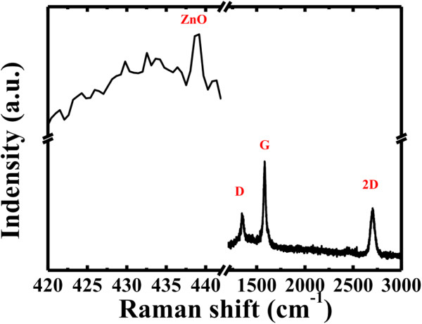
Raman spectroscopy is a promising method for inspecting the ordered/disordered crystal structures of carbonaceous materials and the different layer characteristics of graphene. It was also used to prove that ZnO nanostructures were grown on graphene surface. The usual peak at 437 to 439 cm−1 corresponds to the E2 mode of the ZnO hexagonal wurtzite structure [26]. The G peak at approximately 1,580 cm−1 is attributed to the E2g phonon of C sp2 atoms, and the D peak at approximately 1,350 cm−1 is accredited to local defects and disorder, such as the edges of graphene and graphite platelets [27,28]. Moreover, a 2D peak at approximately 2,700 cm−1 has also been found that may be related to the formation and number of layers of the graphene [29]. Figure 3 shows that the Raman spectrum of the ZnO/graphene exhibits the ZnO peak at 439 cm−1, the D peak at 1,353 cm−1, the G peak at 1,586 cm−1, and the 2D peak at 2,690 cm−1. The formation of few-layer graphene was verified by the intensity ratio of the G peak to that of the 2D peak, which was approximately 1 to 1.5, and by the position of the 2D peak [30,31]. In a word, the characteristics of ZnO and graphene were confirmed by the Raman spectrum.
Figure 3.
Raman spectrum of the ZnO NRs/graphene sheet.
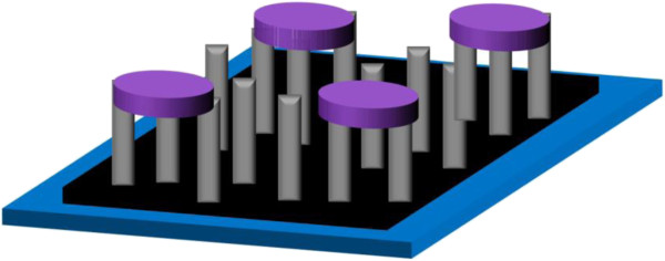
The device structure was fabricated as shown in Figure 4 for Hall measurement. Four electrodes of 200 nm in thickness (100-nm Ti and 100-nm Ag) were located on the four terminals of the ZnO NR layer that was grown on the graphene surface. The electrical conductivity of the ZnO NRs/graphene was obtained and is presented in Table 1. The ZnO film exhibited a high sheet resistance and low charge-carrier mobility before being combined with the graphene sheet. It has previously been discovered that the application of high-mobility graphene is a promising method of addressing this issue of high sheet resistance and low charge-carrier mobility [32]. Therefore, the Hall measurement of the novel hybrid structure, ZnO NRs/graphene on PET, was carried out. The charge-carrier mobility was as high as 124.8 cm2/Vs, 18 times higher than that of the ZnO film. It has been reported that there is an important relationship between mobility and sheet resistance because the carriers can be easily scattered by lattice defects [33]. Accordingly, an enhancement of the mobility would decrease the sheet resistance and thereby promote the electrical conductivity. As a result, a low sheet resistance can be attained because the introduction of a graphene sheet leads to an increase in the overall mobility. Similarly, the stationary electrical performance after bending was an issue of concern. From Table 1, it can be seen that high mobility and low sheet resistance were still observed after bending for 120 repetitions. The hybrid structure of ZnO NRs/graphene has not yet been fully optimized for use as a TCO layer. However, we have demonstrated its great potential for application in optoelectronic devices.
Figure 4.
A schematic illustration of the device fabricated for Hall measurement.
Table 1.
The results of Hall measurements of ZnO and ZnO NRs/graphene on PET substrate
| |
Rs |
Carrier concentration |
Mobility |
|---|---|---|---|
| (Ω cm) | (cm3) | (cm2/Vs) | |
| ZnO |
0.9948 |
1012 |
6.72 |
| ZnO NRs/graphene |
0.2416 |
1012 |
124.8 |
| ZnO NRs/graphene after bending | 0.2426 | 1012 | 120.6 |
Conclusions
Uniform ZnO NRs were obtained by hydrothermal method and grown on a graphene surface that had been transferred to a PET substrate. The ZnO NR/graphene HS exhibited high transmittance (approximately 75%) over the visible wavelength range, even after cyclic bending with a small radius of curvature. Stable electrical conductance of the ZnO NR/graphene HS was achieved, and the improvement of the ZnO sheet resistance by the incorporation of the graphene sheet can be attributed to the resultant increase in carrier mobility.
Competing interests
The authors declare that they have no competing interests.
Authors' contributions
RJC was the principal investigator and is also the corresponding author of this paper. ZCL and PKY were in charge of material preparation and characterization. KYL contributed to data analysis. SFJ and PWC contributed to graphene synthesis. All authors collaborated to complete this research and to compile this manuscript. All authors read and approved the final manuscript.
Contributor Information
Ren-Jei Chung, Email: rjchung@ntut.edu.tw.
Zih-Cian Lin, Email: lzc6991105@hotmail.com.
Po-Kang Yang, Email: d99941008@ntu.edu.tw.
Kun-Yu Lai, Email: kylai@ncu.edu.tw.
Shou-Feng Jen, Email: sofun0920@gmail.com.
Po-Wen Chiu, Email: pwchiu@ee.nthu.edu.tw.
Acknowledgements
The authors are grateful to the part sponsor of this research, the National Science Council of the Republic of China, grants NSC 101-2622-E-027-026-CC3 and NSC 102-2221-E-027-009.
References
- Stutzmann N, Friend RH, Sirringhaus H. Self-aligned, vertical-channel, polymer field-effect transistors. Science. 2003;8:1881–1884. doi: 10.1126/science.1081279. [DOI] [PubMed] [Google Scholar]
- Thomas G. Materials science - invisible circuits. Nature. 1997;8:907–908. doi: 10.1038/39999. [DOI] [Google Scholar]
- Geim AK, Novoselov KS. The rise of graphene. Nat Mater. 2007;8:183–191. doi: 10.1038/nmat1849. [DOI] [PubMed] [Google Scholar]
- Geim AK. Graphene: status and prospects. Science. 2009;8:1530–1534. doi: 10.1126/science.1158877. [DOI] [PubMed] [Google Scholar]
- Yang PK, Chang WY, Teng PY, Jen SF, Lin SJ, Chiu PW, He JH. Fully transparent resistive memory employing graphene electrodes for eliminating undesired surface effects. Proc IEEE. 2013;8:1732–1739. [Google Scholar]
- Tsai DS, Liu KK, Lien DH, Tsai ML, Kang CF, Lin CA, Li LJ, He JH. Few layer MoS2 with broadband high photogain and fast optical switching for use in harsh environments. ACS Nano. 2013;8:3905–3911. doi: 10.1021/nn305301b. [DOI] [PubMed] [Google Scholar]
- Zhang YB, Tan YW, Stormer HL, Kim P. Experimental observation of the quantum Hall effect and Berry's phase in graphene. Nature. 2005;8:201–204. doi: 10.1038/nature04235. [DOI] [PubMed] [Google Scholar]
- Balandin AA, Ghosh S, Bao WZ, Calizo I, Teweldebrhan D, Miao F, Lau CN. Superior thermal conductivity of single-layer graphene. Nano Lett. 2008;8:902–907. doi: 10.1021/nl0731872. [DOI] [PubMed] [Google Scholar]
- He JH, Ho CH. The study of electrical characteristics of heterojunction based on ZnO nanowires using ultrahigh-vacuum conducting atomic force microscopy. Appl Phys Lett. 2007;8:233105. doi: 10.1063/1.2821831. [DOI] [Google Scholar]
- Chao YC, Chen CY, Lin CA, He JH. Light scattering by nanostructured anti-reflection coatings. Energy Environ Sci. 2011;8:3436–3441. doi: 10.1039/c0ee00636j. [DOI] [Google Scholar]
- Ke JJ, Liu ZJ, Kang CF, Lin SJ, He JH. Surface effect on resistive switching behaviors of ZnO. Appl Phys Lett. 2011;8:192106. doi: 10.1063/1.3659296. [DOI] [Google Scholar]
- Tsai DS, Lin CA, Lien WC, Chang HC, Wang YL, He JH. Ultrahigh responsivity broadband detection of Si metal–semiconductor-metal Schottky photodetectors improved by ZnO nanorod array. ACS Nano. 2011;8:7748–7753. doi: 10.1021/nn203357e. [DOI] [PubMed] [Google Scholar]
- Chen CY, Chen MW, Hsu CY, Lien DH, Chen MJ, He JH. Enhanced recovery speed of nanostructured ZnO photodetectors using nanobelt networks. IEEE J Sel Topics Quantum Electron. 2012;8:1807–1811. [Google Scholar]
- Wang GZ, Wang Y, Yau MY, To CY, Deng CJ, Ng DHL. Synthesis of ZnO hexagonal columnar pins by chemical vapor deposition. Mater Lett. 2005;8:3870–3875. doi: 10.1016/j.matlet.2005.07.023. [DOI] [Google Scholar]
- Huang MH, Wu YY, Feick H, Tran N, Weber E, Yang PD. Catalytic growth of zinc oxide nanowires by vapor transport. Adv Mater. 2001;8:113–116. doi: 10.1002/1521-4095(200101)13:2<113::AID-ADMA113>3.0.CO;2-H. [DOI] [Google Scholar]
- Sharma AK, Narayan J, Muth JF, Teng CW, Jin C, Kvit A, Kolbas RM, Holland OW. Optical and structural properties of epitaxial MgxZn1−xO alloys. Appl Phys Lett. 1999;8:3327–3329. doi: 10.1063/1.125340. [DOI] [Google Scholar]
- He JH, Ho CH, Chen CY. Polymer functionalized ZnO nanobelt as oxygen sensors with a significant response enhancement. Nanotechnology. 2009;8:065503. doi: 10.1088/0957-4484/20/6/065503. [DOI] [PubMed] [Google Scholar]
- Yi J, Lee JM, Park WI. Vertically aligned ZnO nanorods and graphene hybrid architectures for high-sensitive flexible gas sensors. Sensor Actuat B-Chem. 2011;8:264–269. doi: 10.1016/j.snb.2010.12.033. [DOI] [Google Scholar]
- Chung K, Lee CH, Yi GC. Transferable GaN layers grown on ZnO-coated graphene layers for optoelectronic devices. Science. 2010;8:655–657. doi: 10.1126/science.1195403. [DOI] [PubMed] [Google Scholar]
- Yin ZY, Wu SX, Zhou XZ, Huang X, Zhang QC, Boey F, Zhang H. Electrochemical deposition of ZnO nanorods on transparent reduced graphene oxide electrodes for hybrid solar cells. Small. 2010;8:307–312. doi: 10.1002/smll.200901968. [DOI] [PubMed] [Google Scholar]
- Choi MY, Choi D, Jin MJ, Kim I, Kim SH, Choi JY, Lee SY, Kim JM, Kim SW. Mechanically powered transparent flexible charge-generating nanodevices with piezoelectric ZnO nanorods. Adv Mater. 2009;8:2185–2189. doi: 10.1002/adma.200803605. [DOI] [Google Scholar]
- Kim YS, Tai WP. Electrical and optical properties of Al-doped ZnO thin films by sol–gel process. Appl Surf Sci. 2007;8:4911–4916. doi: 10.1016/j.apsusc.2006.10.068. [DOI] [Google Scholar]
- Lin YC, Lin CY, Chiu PW. Controllable graphene N-doping with ammonia plasma. Appl Phys Lett. 2010;8:133110. doi: 10.1063/1.3368697. [DOI] [Google Scholar]
- Xu S, Ding Y, Wei YG, Fang H, Shen Y, Sood AK, Polla DL, Wang ZL. Patterned growth of horizontal ZnO nanowire arrays. J Am Chem Soc. 2009;8:6670–6671. doi: 10.1021/ja902119h. [DOI] [PubMed] [Google Scholar]
- Lee C, Wei XD, Kysar JW, Hone J. Measurement of the elastic properties and intrinsic strength of monolayer graphene. Science. 2008;8:385–388. doi: 10.1126/science.1157996. [DOI] [PubMed] [Google Scholar]
- Alim KA, Fonoberov VA, Shamsa M, Balandin AA. Micro-Raman investigation of optical phonons in ZnO nanocrystals. J Appl Phys. 2005;8:124313. doi: 10.1063/1.1944222. [DOI] [Google Scholar]
- Tuinstra F, Koenig JL. Raman spectrum of graphite. J Chem Phys. 1970;8:1126–1130. doi: 10.1063/1.1674108. [DOI] [Google Scholar]
- Ferrari AC, Robertson J. Interpretation of Raman spectra of disordered and amorphous carbon. Phys Rev B. 2000;8:14095–14107. doi: 10.1103/PhysRevB.61.14095. [DOI] [Google Scholar]
- Worsley KA, Ramesh P, Mandal SK, Niyogi S, Itkis ME, Haddon RC. Soluble graphene derived from graphite fluoride. Chem Phys Lett. 2007;8:51–56. doi: 10.1016/j.cplett.2007.07.059. [DOI] [Google Scholar]
- Joly L, Tati-Bismaths L, Weber W. Quantum-size-induced oscillations of the electron-spin motion in Cu films on Co(001) Phys Rev Lett. 2006;8:187404. doi: 10.1103/PhysRevLett.97.187404. [DOI] [PubMed] [Google Scholar]
- Kim KS, Zhao Y, Jang H, Lee SY, Kim JM, Kim KS, Ahn JH, Kim P, Choi JY, Hong BH. Large-scale pattern growth of graphene films for stretchable transparent electrodes. Nature. 2009;8:706–710. doi: 10.1038/nature07719. [DOI] [PubMed] [Google Scholar]
- Bolotin KI, Sikes KJ, Hone J, Stormer HL, Kim P. Temperature-dependent transport in suspended graphene. Phys Rev Lett. 2008;8:096802. doi: 10.1103/PhysRevLett.101.096802. [DOI] [PubMed] [Google Scholar]
- Cullity Deceased BD, Stock SR. Elements of X-Ray Diffraction. 3. New Jersey: Prentice Hall; 2001. [Google Scholar]


