The fabrication and testing of a prototype deep-depletion X-ray CCD are described. Calibration measurements and the results of initial protein crystallography experiments are described.
Keywords: instrumentation, CCD area detectors, protein crystallography
Abstract
The fabrication and testing of a prototype deep-depletion direct-conversion X-ray CCD detector are described. The device is fabricated on 600 µm-thick high-resistivity silicon, with 24 × 24 µm pixels in a 4k × 4k pixel format. Calibration measurements and the results of initial protein crystallography experiments at the Cornell High Energy Synchrotron Source (CHESS) F1 beamline are described, as well as suggested improvements for future versions of the detector.
1. Introduction
Direct-conversion silicon area detectors, in which X-rays are absorbed in a silicon sensor, are excellent devices for synchrotron science owing to their high spatial resolution and to the large number of charge carriers generated per incident X-ray (1 electron–hole pair for every 3.6 eV of deposited X-ray energy; Lutz, 1999 ▶). This leads to a high single X-ray signal-to-noise ratio (SNR) when compared to indirect detection methods, such as phosphor coupling, in which X-rays are stopped in a phosphor that is optically coupled to a conventional CCD that records the resultant visible light.
Direct-conversion silicon X-ray detectors are generally of two types: those in which the silicon X-ray sensor is a separate layer from the processing electronics (herein called pixel array detectors, or PADs), and those in which the sensor and readout electronics constitute a single integrated circuit, such as in direct-detection CCDs. Much detector development has focused on PADs of either the X-ray integrating (e.g. Philipp et al., 2011 ▶; Koerner & Gruner, 2011 ▶; Schuette, 2008 ▶) or the X-ray counting (e.g. Broennimann et al., 2006 ▶; Ballabriga et al., 2007 ▶) variety. However, the pixel size of a PAD is constrained by the need to fit a large amount of signal processing and readout circuitry into each pixel. Typical PAD pixel sizes range from 55 × 55 µm in the Medipix chip (Ballabriga et al., 2007 ▶) to 172 × 172 µm for the PILATUS (Broennimann et al., 2006 ▶). In comparison, the point-spread function in a thick over-depleted silicon sensor is dominated by the diffusion of charge carriers and can have a full width at half-maximum (FWHM) of less than 50 µm, as will be discussed below. Therefore, fabrication of a traditional CCD structure on thick high-resistivity silicon gives a closer match between pixel size and the underlying spatial resolution of the sensor.
Direct-detection CCDs for X-ray astronomy, as well as synchrotron and X-ray free-electron laser (XFEL) science, have been and are currently being developed, typically with 50–450 µm-thick depletion regions (Denes et al., 2009 ▶; Strüder, 2010 ▶; Kiyomichi et al., 2011 ▶). The device described in this paper is a deep-depletion backside-illuminated X-ray CCD fabricated on 600 µm-thick high-resistivity silicon. It has an imaging area of 96 × 96 mm, which is about the maximum size that can be cut from a single 6 inch (∼13 cm) silicon wafer. Results of device characterization and protein crystallography measurements are presented.
2. Device description
The CCD described here, the STA3200, was designed and built by Semiconductor Technology Associates Inc. (STA, San Juan Capistrano, CA, USA). The wafer processing was done by Teledyne DALSA (Waterloo, Ontario, Canada) in a standard NMOS buried-channel triple poly/double metal CCD process. Readout is controlled by four-phase parallel registers, clocked at 300 kHz, and three-phase serial registers, clocked at 5 MHz. The parallel registers have metal strapping on the polysilicon gates to reduce the gate resistance and improve the performance at high speeds. The serial register is widened to increase the binned well depth and can accommodate almost twice the single-pixel full well. There are eight output amplifiers on the top and bottom edges, for a total of 16. A frame can be read out either in a split-frame configuration through all 16 ports or through the eight ports on either side. A defect in one amplifier on the current chip makes eight-port readout necessary in order to capture the full imaging area. The detector was operated in full-frame mode with eight-port readout in all measurements described in this paper.
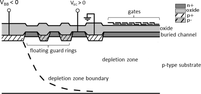
The diode structure is sketched in Fig. 1 ▶. The 600 µm-thick silicon should provide 84% efficient X-ray stopping power at 13.5 keV. The material is p-type float-zone silicon and has a resistivity of >10 kΩ cm, as stated by the manufacturer. It was found that the clock feed-through noise could be significantly reduced by gating the reverse bias such that the full bias is only applied during the integration period, gating it off during readout. The device is intended to be run with a reverse bias (V BB) sufficiently large to over-deplete the sensor. Initial testing showed full depletion at 300–325 V reverse bias as shown by the single-photon response of X-rays from a weak 55Fe source. After these initial tests, the onset of electrical breakdown was observed at a reverse bias of 170 V and the CCD could no longer be operated in full depletion. The cause appears to be damage to the electrical guard ring structure on the surface of the CCD. Therefore, unless otherwise noted, the measurements described in this paper were carried out at a reverse bias of 155 V.
Figure 1.
The CCD diode structure. X-rays enter from the back side (shown at the bottom). The current design includes eight floating guard rings; fewer are shown for simplicity.
A 300 V minimum depletion bias would correspond to a resistivity of approximately 11.4 kΩ cm. At this resistivity, a reverse bias of 155 V would deplete a 430 µm thickness within the wafer, leaving a 170 µm-thick undepleted region at the X-ray entrance side. Having an undepleted region will affect both the efficiency and the resolution, as discussed below.
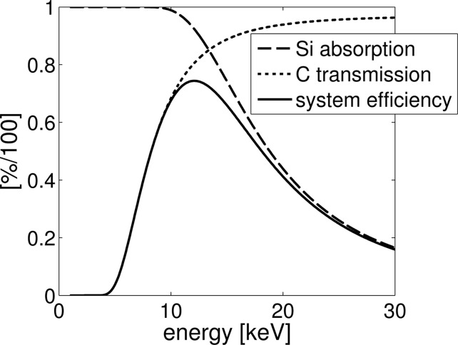
The chip is cooled to 205 K using a Cryotel closed-cycle cryocooler (Sunpower, Athens, OH, USA). The X-ray vacuum window of the detector consists of a 0.79 mm-thick epoxy-carbon fiber fabric. Although the window absorption lowers the system efficiency to 72% at 13.5 keV, the window was inexpensive and served well for the testing purposes of this report. However, the carbon window attenuates lower energies more severely (Fig. 2 ▶), and should be replaced with a beryllium window for use with lower-energy X-rays.
Figure 2.
Nominal detector, window and system efficiencies as a function of X-ray energy.
The detector is controlled over a CameraLink interface. Signals sent over CameraLink from the control computer are relayed through a backplane to a set of bias, clocking and A/D printed circuit boards. Both continuous framing and immediate trigger modes are provided. The trigger can be provided through software or by a hardware transistor–transistor logic signal. Vertical binning is available on-chip. Fig. 3 ▶ shows a photograph of the prototype device, as well as a photograph of the bare CCD on its headboard.
Figure 3.
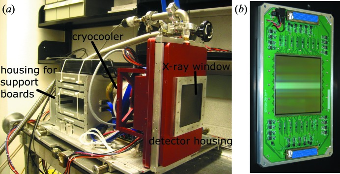
(a) The direct-detection CCD with detector housing, cryocooler and support electronics. (b) The bare CCD on its headboard.
3. Charge collection and diffusion in silicon
In the absence of an electric field, free charge carriers in silicon move diffusively with diffusion constant 
 , where k
B is the Boltzmann constant, T is the temperature, q is the electrical charge of the charge carriers and μn/p is the electron/hole mobility. In this device, electrons are collected at the CCD gates, so throughout this paper we will use μn. In the presence of an electric field, charge carriers drift with equation of motion
  .
.
By design, in this and other deep-depletion silicon sensors, the full sensor volume should be over-depleted, such that there is a strong transverse electric field across the sensor, sweeping photo-generated charges rapidly towards the pixel gates. This leads to short collection times, of the order of 10 ns. Ideally, there is no lateral electric field, and the lateral charge profile can be modeled as a Gaussian with a width of  , or about 10 µm for t = 10 ns at room temperature. The electron mobility scales with temperature as T
−2.42 (Jacoboni et al., 1977 ▶).
In the prototype CCD described here, electrical damage constrained us to operate the device in a partially depleted state. It is possible for X-ray photons to be stopped and converted into charge in the undepleted layer. The probability of this occurring depends on the X-ray energy and is greater for lower energies. If an X-ray is stopped in the undepleted field-free region, the photo-charge will spread diffusively in three dimensions until it either enters the depleted region or recombines. The recombination time within silicon varies, depending on the defect density, from nanoseconds to milliseconds. Minority carrier lifetimes between 2 and 6 ms are typical in high-resistivity float-zone silicon (Dreier, 1990 ▶). Photo-charge generated in the undepleted region that does reach the depletion region before recombination will be collected, but potentially by a pixel some distance away from the location of the photon hit. Therefore, the presence of the undepleted layer has implications for the spatial resolution and efficiency of the CCD, as will be discussed in the next section.
This model provides a qualitative understanding of the effects of partial depletion. It is not our intention to rigorously characterize the motion of charge in the undepleted region, since the presence of an undepleted region in this prototype is a flaw that should not be repeated. As will be discussed in §6, future revisions of this device would include an improved guard ring structure that would allow the chip to be operated in over-depleted mode.
The extent to which the undepleted layer impacts on device performance depends on its thickness relative to the depleted layer. As described above, 55Fe testing showed evidence of full depletion around 300 V, indicating an 11.4 kΩ cm resistivity and a 170 µm undepleted layer at the operating reverse bias. Because the electrical damage prevented us from rigorously verifying that 300 V is the absolute minimum bias required for full depletion, we consider this a lower bound on the resistivity and an upper bound on the undepleted thickness. As will be discussed in §4.3, efficiency measurements provided a lower bound on the undepleted thickness.
4. Characterization measurements
The detector characteristics are summarized in Table 1 ▶. The calibration measurements are described below. Visible light measurements were made using an LED placed within the detector housing. The X-ray calibration measurements were carried out using copper and molybdenum anode X-ray tubes (TruFocus, Watsonville, CA, USA), with 180 µm source size. The distance between the detector window and the X-ray source, or between the mask and the X-ray source where a mask was used, was 1 m, unless otherwise noted. The surface of the CCD is 19 mm behind the detector window.
Table 1. Summary of detector characteristics.
| Quantity | Value |
|---|---|
| Pixel size | 24 × 24 µm |
| Format | 4000 × 4000 pixels |
| Frame rate | 1.6 Hz in 8-port readout (625 ms read time), 3.2 Hz in 16-port readout (310 ms read time) |
| Read noise | 3 ADU (0.10 photons at 13.5 keV equivalent) |
| Pixel well depth | 1.4 Me− (373 photons at 13.5 keV equivalent) |
| Serial register well depth | 2.2 Me− |
| Gain | 128.2 e− ADU−1 (29.2 ADU photon−1 at 13.5 kev equivalent) |
| Dark current | 22 e− s−1 at 205 K |
| Point-spread function FWHM | 22 µm (at 17.5 keV), 40 µm (at 8.0 keV) |
4.1. Visible light measurements
Many CCD system parameters can be extracted by examining the visible light photon transfer curve (the curve of signal variance as a function of illumination level) (Janesick, 2001 ▶). Since each visible photon generates no more than a single electron, the variance in the recorded signal goes as the number of electrons recorded, yielding a direct measurement of system gain. These measurements show a system gain of 128.2 e− per analog–digital unit (ADU), with a read noise of 380 e− r.m.s. The full-well capacity per pixel was measured to be 1.4 × 10⁶ e−. Dark current measurements show a linearity of <1.5% over the full range. Since X-rays produce an electron–hole pair for each 3.6 eV deposited in the silicon, a single 13.5 keV X-ray would generate 3750 e−. Expressing the CCD parameters in terms of 13.5 keV X-rays, the system gain would be 29.2 ADU per X-ray, with a read noise of 0.10 X-rays and a full-well capacity of 373 X-rays. Parameters at other X-ray energies would scale directly as the X-ray energy.
The gain variation between amplifier readouts was measured to be 1.86% r.m.s. and can be corrected by applying a multiplicative factor.
4.2. X-ray gain measurement
The gain of the CCD can also be measured by generating a histogram over many frames of photon hits in a specified area illuminated under low-flux conditions. This histogram is composed of a series of discrete photon peaks, corresponding to zero photon hits, one photon hit and so on. The detector gain determines the spacing between the discrete photon peaks. This method has been used to calibrate the pixel gain in photon-integrating PADs, where X-ray pinholes were used to isolate individual pixels, each of which has its own readout amplifier (Schuette, 2008 ▶).
An X-ray-opaque mask fabricated in 50 µm-thick tungsten with a square array of 25 µm-diameter pinholes on a 330 µm pitch was used to produce isolated spots of illumination on the detector. The mask was flood illuminated using a molybdenum anode tube, biased at 25 kV and 0.078 mA. A 200 µm-thick zirconium foil was placed directly in front of the X-ray source to improve the spectral purity and isolate the 17.5 keV Mo Kα line. A set of 50 5 s frames were taken, with about two photons on average incident through a single pinhole per frame.
Since the illumination from a single pinhole is not necessarily confined to a single pixel, multiple pixels must be summed in order to fully capture the intensity from each spot. Since each pixel in the sum contributes read noise, care is required in defining the area to be summed, as the minimum area that encompasses the signal should be used. To do this, the center of mass of each pinhole was determined from the averaged background-subtracted image. For a given radius r, pixels in the neighborhood of a pinhole were flagged if any fraction of their area fell within a circle of radius r centered on the pinhole center of mass, as illustrated in Fig. 4 ▶. In each frame, the flagged pixels were summed to obtain the pinhole intensity.
Figure 4.
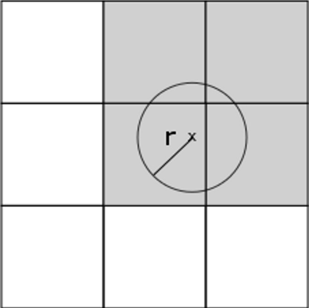
A block of 3 × 3 pixels is shown to illustrate the area summation operation. The center of mass of the pinhole is marked by an ‘×’. A circle of radius r is drawn centered on the pinhole center of mass. If any fraction of a pixel’s area falls within the circle, the pixel is included in the intensity sum.
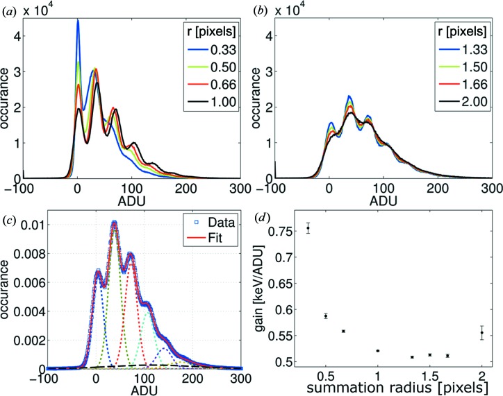
Figs. 5 ▶(a) and 5 ▶(b) shows the spectra obtained for r ranging from 0.33 to 2.00 pixels. As the radius is increased, the photon peaks broaden as additional read noise is incorporated into the sum. The photon peak spacing initially increases as the radius increases to about 1 pixel, then levels off, suggesting that most of the pinhole intensity is captured by the sum with r in the range of 1–1.5 pixels.
Figure 5.
(a), (b) The discrete photon spectra obtained by summing pixels within a radius of 0.33–2.00 pixels of the pinhole center of mass. The results are split into two plots for clarity. (c) The fit to a sum of Gaussians is shown for r = 1.50 pixels. The dotted lines show the individual discrete photon peaks and the dashed black line is the background Gaussian. (d) The computed gain from the fit is plotted as a function of the summation radius.
To compute the gain, the spectra are fitted to a sum of N + 2 Gaussians, corresponding to the zero-photon peak, N discrete photon peaks and a diffuse peak that accounts for the tails of the distribution, with the detector gain as a fit parameter. The fit for r = 1.5 pixels is plotted in Fig. 5 ▶(c). The computed gain is plotted as a function of summation radius in Fig. 5 ▶(d). The computed gain levels off to 34.5 ADU per 17.5 keV photon for r = 1.33–1.66 pixels. The measurement at a radius of 2 pixels is more uncertain owing to increased read noise introduced into the sum.
Since one electron–hole pair is generated for every 3.6 eV deposited in the detector, a gain of 34.5 ADU per 17.5 keV photon corresponds to an energy-independent conversion factor of 140 e− ADU−1. This agrees well with the measurement made with visible light to within 10%. The agreement between visible light and X-ray measurements confirms that the parameters extracted from the visible light data are valid when extrapolated to the X-ray regime. Note that X-ray spectral peaks at lower X-ray energy broaden because of the higher proportion of photons converting in the undepleted zone. Both the increased lateral spread and the loss of charge due to recombination cause these photon peaks to no longer be well resolved.
4.3. X-ray efficiency
The efficiency of the CCD was determined by comparing the signal measured by the CCD with that from a calibrated silicon drift detector (SDD). Both the CCD and a Vortex-90EX SDD (SII NanoTechnology USA Inc., Northridge, CA, USA) were illuminated through a 1.9 mm2 lead aperture with either a copper or a molybdenum X-ray tube. Both sources were filtered to improve spectral purity: the Cu tube with a 50 µm-thick Ni filter, and the Mo tube with a 75 µm-thick Zr filter combined with a 1 mm-thick Al filter. The latter configuration provides similar transmission, especially at high energies, to the 200 µm Zr filter described above, with the main difference being decreased transmission of the Kα line.
The number of counts per second in the Kα line of each source was calculated from the SDD data, using an equivalent carbon fiber window to that on the CCD. The efficiency of the SDD sensor was determined experimentally by measuring the increase in recorded signal as the SDD was tilted with respect to the incoming beam, thus changing the apparent sensor thickness by a known factor. The SDD sensor thickness was calculated to be 287 µm (+27 or ∼29 µm). Using the gain computed from the photon transfer curve, the signal recorded by the CCD was converted to a number of photon counts per second. The ratio of the measured to expected flux gives the CCD efficiency: approximately 0.55 (− 0.09 or + 0.07) at 17.5 keV and 0.47 ± 0.01 at 8.0 keV.
If the CCD were fully depleted, the efficiency would be 0.58 at 17.5 keV and nearly 1 at 8.0 keV. The efficiency measured for 17.5 keV X-rays agrees with this expectation within the uncertainty of the measurement. The loss of efficiency at 8.0 keV indicates that the CCD is not fully depleted. Since the CCD depletes from the p–n junction at the front side, under-depletion would result in an undepleted layer at the back side (i.e. the X-ray entrance side). X-rays could still be stopped and converted into charge in the undepleted layer, but the photo-generated electrons would be more likely to be lost to recombination. There would also be a loss of spatial resolution, due to the absence of a strong electric field to sweep the photo-generated charge towards the CCD gates, i.e. photo-generated charges that did survive long enough to reach the depletion zone would have time to diffuse laterally away from the interaction point. The undepleted layer could therefore be partially collecting. If the undepleted layer were approximated as a purely attenuating dead layer, the efficiency measurements would suggest a thickness of ∼55 µm at the operating reverse bias of 155 V. This gives a lower bound on the thickness of the undepleted layer.
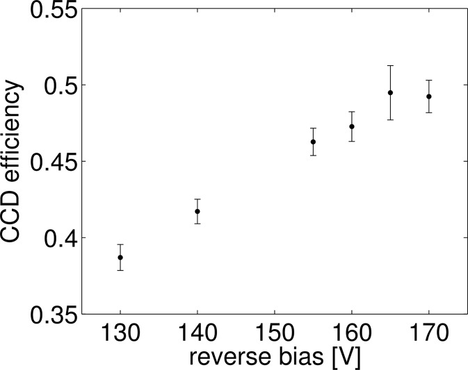
The effect of the reverse bias on the collection efficiency was probed by repeating the measurement for Cu Kα radiation over a range of reverse-bias settings. The measured efficiency is plotted in Fig. 6 ▶. The curve shows a growing depletion thickness with increasing bias. However, the loss of efficiency at 170 V suggests that the CCD is still far from fully depleted. At 170 V and above a sharp increase in current draw on the reverse-bias supply, combined with an increase in dark current around the chip edges, indicated the onset of electrical breakdown in the chip. The cause appears to be damage to the electrical guard ring structure on the surface of the CCD. While this constrained the reverse bias that could be applied, it allowed sufficient depletion of the CCD for the characterization of this report.
Figure 6.
The CCD efficiency at 8.0 keV versus reverse bias.
4.4. Spatial resolution
In a direct-conversion device, the point spread is determined by the lateral diffusion of charge carriers as they traverse the diode. As discussed in §3, the lateral spread of charge during time t can be modeled as a Gaussian with standard deviation  . The transit time t depends on the electric field present in the sensor and therefore on the reverse-bias voltage. In the ideal case of an over-depleted sensor, the lateral charge carrier diffusion is limited by reducing the time required to sweep the charge carriers across the diode.
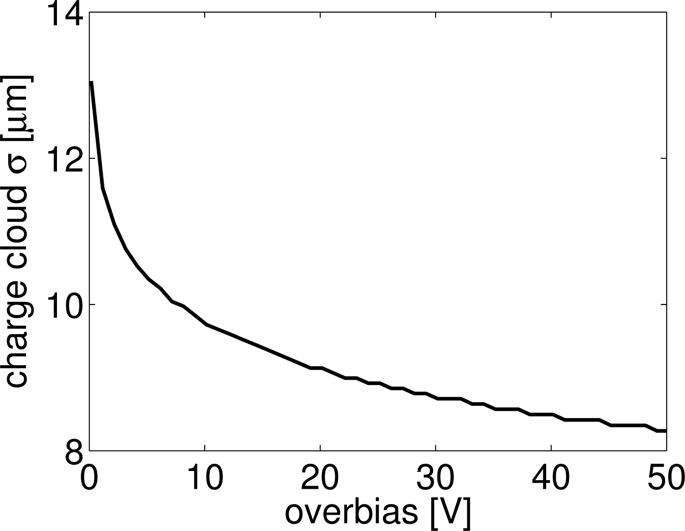
As a test case, we consider the lateral charge spread in a 10 kΩ cm 600 µm-thick fully depleted sensor cooled to 205 K. We model the scenario where the X-ray is absorbed at the back surface of the sensor, which gives the longest transit time and therefore an upper bound on the lateral spread of the charge cloud. This calculation does not take into account inter-charge repulsion or local field variations, which in an over-depleted sensor will be weak compared to the reverse-bias field. The results obtained give an estimate of the point spread that can reasonably be achieved with a 600 µm-thick fully depleted silicon sensor. The standard deviation of the Gaussian charge cloud is plotted as a function of overbias voltage in Fig. 7 ▶. A σ of 10 µm is expected at 10 V overbias, i.e. an applied bias of approximately 350 V. The support electronics for the CCD were chosen to accommodate an applied bias of 500 V. However, in the current prototype, the power supply draw became unstable above a reverse bias of 155 V.
Figure 7.
The charge cloud width versus overbias of a 600 µm 10 kΩ cm diode.
To characterize the spatial resolution of the CCD, the response to knife-edge illumination was measured. A 1 mm-thick tungsten knife edge was placed within 4 mm of the CCD window and was aligned with the charge transfer axis of the CCD, then tilted by approximately 2° using a rotation stage. The knife edge was illuminated by an Mo tube biased at 25 kV and 0.142 mA, filtered by a 200 µm-thick Zr foil. A set of 50–60 s exposures was averaged to obtain the final knife-edge image. A complementary data set was taken with the knife edge oriented slightly off-axis in the direction perpendicular to charge transfer. The measurement was repeated using a Cu tube, biased at 15 kV and 0.6 mA, with a 50 µm-thick Ni filter.
Tilting the knife edge has the same effect as aligning the knife edge parallel to the direction of measurement and capturing frames at perpendicular translations of psin(θ), where p is the pixel pitch and θ is the angle by which the knife edge is tilted from the axis. By plotting the intensity along a row or column that the knife edge crosses, the edge-spread response (ESR) of the device is obtained (Fig. 8 ▶).
Figure 8.
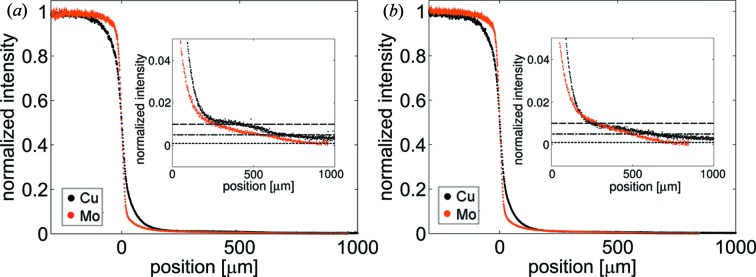
(a) The edge-spread response of the CCD parallel to the charge transfer direction. (b) The edge-spread response perpendicular to the charge transfer direction. The 1, 0.5 and 0.1% levels are indicated by dashed lines in the insets.
For 17.5 keV (Mo Kα) radiation, the ESR is similar in both directions. The most notable feature of the measured ESR is the long tail in the non-illuminated region. The intensity falls off to the 10% level at 20 µm from the knife edge, to the 1% level at 300 µm, to the 0.5% level at 500 µm and to the 0.1% level at 800 µm.
For 8.0 keV (Cu Kα) radiation, the long-range spread is greater. The intensity falls off to the 10% level at 55 µm from the knife edge in both directions, to the 1% level at 300 µm from the edge in the perpendicular direction and 400 µm in the parallel direction, and to the 0.5% level at 650 µm in both directions. Elevated dark current near the chip edges corrupts the response curve before the 0.1% level is reached.
The long tails of the edge-spread response, and the dependence on energy, again indicate that the detecting volume is not fully depleted. As discussed in §3, when photons are stopped in the undepleted layer, there is no electric field to sweep the charge carriers efficiently towards the CCD gates. Instead, the charge produced diffuses in three dimensions but in this case the lateral spread can be significant by the time the charge reaches the depletion region. Charge carriers that reach the depletion region before recombining will be swept to the CCD gates by the reverse-bias field, but will be collected by pixels potentially far away from the original photon hit. A greater portion of the incident radiation will be stopped in the dead layer at 8.0 keV than at 17.5 keV. Given the observed lateral charge spread of several hundred micrometres, recombination lifetime must exceed a few microseconds. This is well within the electron lifetime possible in high-purity float-zone silicon (Dreier, 1990 ▶).
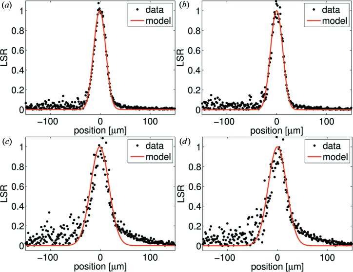
By differentiating the ESR, the line-spread response (LSR) is obtained, as shown in Fig. 9 ▶. The LSR is the response of the sensor to an infinitely thin line of illumination and is equivalent to a one-dimensional slice through the point-spread function. The LSR was modeled as a convolution of a Gaussian, representing the diffusion of charge in the sensor, with a boxcar function representing the 24 µm pixelation. This model gave a best-fit charge diffusion FWHM of 22 µm for Mo Kα radiation and 40 µm for Cu Kα radiation. Though the data deviate from this model at the low-intensity tails, the fit is reasonable at the FWHM level.
Figure 9.
(a) The LSR perpendicular to charge transfer with Mo radiation. (b) The LSR parallel to charge transfer with Mo radiation. (c) The LSR perpendicular to charge transfer with Cu radiation. (d) The LSR parallel to charge transfer with Cu radiation. Each measured curve is shown along with the best fit model.
4.5. Uniformity of response
In addition to fixed pattern noise and cosmetic defects, flood-field illumination of the CCD shows characteristic ‘tree ring’ variations (Fig. 10 ▶). Radial resistivity variations of the order of 20% are typical in high-resistivity float-zone silicon (von Ammon & Herzer, 1984 ▶). The silicon used in this device has a stated radial resistivity tolerance of 25%. The resistivity variation is due to doping inhomogeneities in the boule from which the wafer is cut, which are in turn caused by convection patterns that form when portions of the boule are melted during refinement (Dreier, 1990 ▶). The doping inhomogeneities produce lateral fields that deflect charge as it traverses the diode, altering the effective collection area of a given pixel. This results in a tree ring pattern in areas of nominally flat illumination. This effect is seen in practically all other area detectors based on thick high-resistivity silicon sensors, including silicon drift detectors on both float-zone silicon (Vacchi et al., 1991 ▶) and neutron transmutation doped silicon (Nouais et al., 2001 ▶; Crescio et al., 2005 ▶; Batigne et al., 2008 ▶), pixel array detectors with sensors made from float-zone silicon (Tlustos, 2005 ▶; Schuette, 2008 ▶; Green et al., 2013 ▶), and other deep-depletion CCDs fabricated on float-zone silicon (Kotov et al., 2011 ▶). All of the detectors referenced above are run fully or over-depleted, in which case the tree rings can be fully attributed to lateral area distortions. Here, because the CCD is under-depleted, the doping inhomogeneities may also lead to local efficiency variations which contribute to the tree ring pattern. In the under-depleted case, the tree rings are most likely to be due to a superposition of lateral deflection and efficiency variation. Note that, since the CCD is cut to the maximum size allowed by a 6 inch wafer, the full tree ring structure of the wafer is visible, whereas in smaller devices, a single sensor includes only a slice of the pattern from the source wafer.
Figure 10.

(a) A Cu Kα flood field. (b) An Mo Kα flood field. (c) An azimuthal integration of both flood fields, centered on the tree ring structure. An annulus width of 1 pixel was used.
The magnitude of distortions depends on several factors, including the angle of incidence, the conversion depth and the X-ray energy. The dependence on X-ray energy is illustrated in Figs. 10 ▶(a) and 10 ▶(b), which show a Cu Kα flood field and an Mo Kα flood field, respectively. The flood fields were taken using a Cu tube, biased at 18 kV and 0.4 mA, at a distance of 1.5 m from the detector window, and an Mo tube, biased at 25 kV and 0.6 mA, with a 200 µm-thick Zr filter, at a distance of 1 m from the detector window. The tree ring structure is more distinct in the Cu Kα flood field but is present in both images. An irregularly shaped region of increased intensity covering most of the chip is visible in the Mo Kα flood field. Because of its shape, we suspect this is visible fluorescence from the thermal grease (Apiezon N; M & I Materials Limited, Manchester, UK) between the CCD chip and the aluminium cold plate. Apiezon N has been shown to fluoresce in the blue under UV light (Cooke & Bennett, 1996 ▶). Clearly, a nonfluorescent thermal coupling compound should be used for future work.
An azimuthal integration of each flood field is plotted in Fig. 10 ▶(c) as a function of radial distance r chip from the center of the chip. At around r chip = 1500 pixels, in the Mo Kα flood field, the thermal grease fluorescence falls off, leading to a large downward shift in the intensity curve that is independent of the tree rings. Since the fluorescence fall-off is a separate effect from the tree rings, in order to compare the tree ring effects in the sensor in the Mo and Cu Kα flood fields, we focus on the inner region of the chip (r chip = 0–1500 pixels). Within this region, there are three significant dips in the intensity curve, indicated by arrows in Fig. 10 ▶(c). These features correspond to dark rings in the flood images. The maximum peak-to-peak excursion in this region is 1.5% in the Mo Kα flood field and 2.7% in the Cu Kα flood field. The r.m.s. variation in the inner region is 0.2% for the Mo Kα flood field and 0.7% for the Cu Kα flood field.
4.6. Radiation damage
Radiation damage measurements were carried out on an STA 1759A imager similar in design to the current prototype. The STA 1759A chips were 250 µm thick and were illuminated from the front (gate) side. The benefit of performing radiation damage testing on a front-illuminated device is that it is much easier to observe the effect of radiation on the oxide, whereas in a thick back-illuminated device, the gate oxide is shielded by the thick Si detecting layer. The creation of electron–hole pairs in the oxide is a primary source of radiation damage in CCDs (Janesick, 2001 ▶). Within the oxide, photo-generated holes become trapped owing to their low mobility, which generates a flat-band voltage shift that can eventually push the CCD out of its operational region. At the Si–SiO2 interface, trapped charge can generate an additional voltage shift, as well as increasing the dark current generated at the interface.
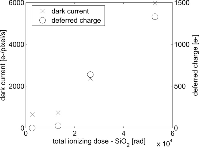
The test devices were cooled with liquid nitrogen to 213 K and were biased and clocked as in normal operation during radiation damage testing. 8.0 keV Cu Kα X-rays were generated by a rotating anode and isolated by a multilayer monochromator. The dose rate was measured to be 78 rad s−1 in Si and 44 rad s−1 in SiO2 (1 rad = 0.01 Gy). Dark current and deferred charge, a measure of charge transfer efficiency (CTE) degradation, were monitored as the devices were dosed. The results are shown in Fig. 11 ▶. A slight (6%) increase in dark current was detected at the lowest dose level recorded, 2640 rad (SiO2). CTE degradation was detected at 13 200 rad (SiO2).
Figure 11.
Dark current and deferred charge are plotted as a function of oxide dose.
5. Protein crystallography
Protein microcrystallography is the target application for the direct-detection CCD. The average diffraction peak intensity from a crystal of volume V and unit-cell volume V C is governed by Darwin’s formula and scales as V/V C 2 (Drenth, 1999 ▶). Therefore, small crystals with large unit cells, as found for macromolecular proteins, diffract weakly. To make the most out of weakly diffracting samples, methods are being developed to maximize the beam intensity incident on the crystal and to minimize the background scattering.
On a synchrotron beamline, the incident intensity can be maximized by focusing the beam down to 20 µm or less, to match the size of the microcrystal. An overview of focusing technologies as applied to microcrystallography has recently been published (Smith et al., 2012 ▶). Matching the beam size to the crystal size naturally reduces background scatter by limiting the amount of extraneous material hit by the direct beam. The sample environment can be tailored to reduce background scatter further, by systematically removing potential scatterers from the path of the direct beam. Air scatter can be reduced by limiting the volume of air through which the direct beam travels: for example, by placing the beamstop very close to the sample, or through the use of vacuum or helium flight paths. Scatter from vacuum windows can be reduced by using ultra-thin low-density window materials, such as a 100 nm silicon nitride film. Microfabricated polyimide mounts can be used in place of nylon loops to mount small crystals (Thorne et al., 2003 ▶). These sample mounts produce low background scatter themselves compared to nylon loops, and also limit the amount of liquid surrounding the crystal.
It follows that the detector chosen for a protein microcrystallography experiment should contribute minimal noise and should preserve the signal incident on the detector plane as faithfully as possible, i.e. the detective quantum efficiency (DQE) should be maximized. The DQE is defined as (S o/N o)2/(S i/N i)2, where S o/N o is the signal-to-noise ratio at the detector output and S i/N i is the signal-to-noise ratio at the detector input, and is a measure of the detector’s contribution to the overall SNR. The tight point spread and small pixels of the direct-detection CCD ensure that the spatial characteristics of the diffraction pattern are preserved faithfully and that weak Bragg spots are not washed out by a large point spread. Additionally, the large number of charge carriers generated per X-ray photon makes the pixel read noise (3 ADU, equivalent to 385 electrons) equivalent to about 1/10 of a 13.5 keV photon. This combination of high spatial resolution and low read noise increases the detector SNR and makes the device uniquely suited to this class of experiments.
A series of protein crystallographic data sets were taken at the F1 beamline at CHESS to examine the detector performance. Data were also collected on a Quantum 270 (Q270) CCD (Area Detector Systems Corporation, Poway, CA, USA), for direct comparison. The Q270 is an indirect-detection device, in which X-rays are stopped in a phosphor coupled via a fiber optic taper to conventional CCD chips. The Q270 has 64.8 × 64.8 µm pixels at the phosphor surface. As reported by the manufacturer, the spatial resolution FWHM is 90 µm, and the read noise is equivalent to about 1/2 of a 12 keV photon. The readout time in the unbinned mode used here is 1.1 s.
The direct-detection CCD was mounted on a vertical translation stage just below the Q270, allowing a rapid switch between the two detectors in order to collect comparable data sets on both detectors. The beamline energy was 13.5 keV. The samples were flash-frozen thaumatin crystals in 20% glycerol (Ko et al., 1994 ▶). All crystals had dimensions in the range 60–100 µm. The crystals were mounted in nylon loops and held in a cold stream at 100 K.
Four different experimental configurations were tested: a 100 µm beam with the detectors at equal distance from the sample, a 100 µm beam with equal solid angle per pixel per detector, a 20 µm beam with equal distance and a 20 µm beam with equal solid angle per pixel. The 100 µm beam was produced with a simple collimator. The 20 µm beam was produced using a single-bounce focusing capillary (Huang & Bilderback, 2006 ▶). Because of the relatively small size of the direct-detection CCD, it was necessary to place that detector very close to the sample in order to span an acceptable q range. For the equal-solid-angle experiments, the direct-detection CCD was placed 113 mm from the sample; the Q270 was placed 292 mm from the sample. For the equal-distance experiments, a sample-to-detector distance of ∼150 mm was chosen to accommodate physical constraints that prevented us from moving the Q270 closer to the sample. Exposures were 1 s with a 1° oscillation per frame. The exposure time was chosen to limit the number of overexposed reflections.
Crystallographic analysis was performed using MOSFLM (Leslie & Powell, 2007 ▶) and SCALA (Evans, 2006 ▶). The results for the four different configurations are shown in Table 2 ▶. Data quality was assessed by evaluating R merge, a measure of the agreement of Bragg reflections across multiple measurements, defined as
in which I hkl,i is the ith measurement of reflection hkl and 〈Ihkl〉 is the average intensity of the reflection (Evans, 2006 ▶). In all but one case, the direct-detection CCD data resulted in a lower R merge than that obtained using the Q270. The difference is greater if only full reflections are included in the calculation; owing to timing jitter in the triggering interface between the beamline and the direct-detection CCD, some partially recorded reflections had slight tails due to the shutter being open during read-out.
Table 2. Summary of protein diffraction results from the two detectors.
Thau6 and Thau9 are nominally equal distance data sets. R merge(fulls) is R merge computed using only reflections that are fully recorded on a single frame.
| Crystal | Mosaicity (°) | Beam size (µm) | Detector | Distance (mm) | R merge | R merge(fulls) |
|---|---|---|---|---|---|---|
| Thau9 | 0.56 | 100 | Q270 | 148 | 0.093 | 0.070 |
| STA3200 | 153 | 0.056 | 0.038 | |||
| Thau6 | 0.35 | 20 | Q270 | 148 | 0.104 | 0.090 |
| STA3200 | 153 | 0.100 | 0.067 | |||
| Thau13 | 0.82 | 100 | Q270 | 292 | 0.092 | 0.065 |
| STA3200 | 113 | 0.115 | 0.088 | |||
| Thau4 | 0.30 | 20 | Q270 | 292 | 0.106 | 0.092 |
| STA3200 | 113 | 0.095 | 0.069 |
In the case of Thau13, the only data set for which the Q270 had better statistics than the STA3200, the diffraction spots on both detectors showed evidence of splitting. We speculate that this may be a scenario where it is preferable to resolve less detail within the Bragg spots and that this may account for the hampered performance of the direct-detection CCD.
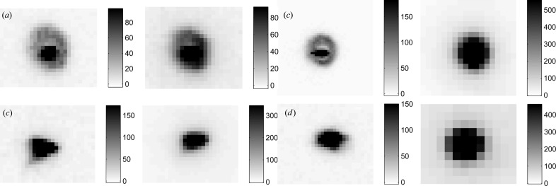
As a result of the tighter point-spread function and smaller pixels, finer detail was seen in the direct-detection CCD data than in the Q270 data. Some representative examples are shown in Fig. 12 ▶. One feature immediately obvious to the eye is the greater detail visible in the Bragg spots on the direct-detection CCD, particularly in the 20 µm beam data. The details within the Bragg spots are true features reflecting the beam profile and crystal shape. Details within Bragg spots have been used in XFEL experiments to recover information about the crystal shape (Chapman et al., 2011 ▶).
Figure 12.
Diffraction spots used for detector comparison. Each pair of images represents a different experimental configuration: (a) 20 µm beam, equal solid angle per pixel (crystal Thau4); (b) 20 µm beam, equal distance (Thau6); (c) 100 µm beam, equal solid angle per pixel (Thau13); (d) 100 µm beam, equal distance (Thau9). In each pair, the left image is from the direct-detection CCD and the right is from the Q270. In each pair, the same approximate solid angle is displayed; in (a) and (c), this results in the same number of pixels in each image, whereas in (b) and (d), fewer pixels are spanned on the Q270 than on the direct-detection CCD, which makes the pixels appear larger when printed. All images are scaled such that the grayscale maximum is 30% of the maximum value in the region of interest. The grayscale is cast in units of photons, as shown in the scale bar alongside of each image. The halo structure observed in (a) and (b) is a consequence of the glass X-ray capillary used to focus the beam. It arises from the divergence in the 20 µm beam, which is focused at the sample position and has expanded considerably at the detector position.
6. Design goals and lessons
The current prototype device exhibits a point spread of the order of 22–40 µm FWHM and a pixel read noise equivalent to 1/10 of a photon at 13.5 keV, and, even given known flaws, performs successfully in the context of protein crystallography. However, further development would improve the frame rate and support electronics, and would eliminate the undepleted layer on the X-ray entrance side of the diode. Thus, the results of the prototype studies have laid the foundation for modifications to future improved device performance. Lessons for further development are described below.
6.1. Undepleted layer and biasing
The undepleted layer is the greatest drawback to the current prototype, leading to loss of efficiency and spatial resolution. The onset of electrical breakdown at the relatively low reverse bias of 170 V needs to be resolved so that the chip can be fully depleted. The early onset of breakdown suggests that the guard ring structure has been damaged. The guard rings in the current prototype are 15 µm wide with 6 µm gaps between rings. An inter-ring gap of the order of 20–30 µm would be more robust.
6.2. Frame rate
The current maximum frame rate is ∼3 Hz. Higher frame rates could be achieved by increasing either the serial register clock frequency or the number of readout amplifiers. At the current clock frequency and chip size, increasing the number of amplifiers per side from 8 to 32 would result in a maximum frame rate of 20 Hz. A potential drawback to increasing the number of amplifiers on a large device is a decrease in yield due to amplifier failure. STA has been able to mitigate this risk through the use of in-process gettering to reduce the defect density and by re-designing the amplifier gates to minimize voltage breakdown. A 36 × 36 mm chip with 56 output amplifiers has recently been developed.
Alternatively, to reduce the noise penalty associated with an increase in clock speed, there are two possible approaches. First, the support electronics could be redesigned so that the CCD output is digitized on the headboard in close physical proximity to the chip outputs; currently digitization takes place on A/D boards connected to the CCD headboard by long (0.3 m) readout cables. This could reduce clock feed-through noise and allow the serial register clock frequency to be increased, without redesigning the chip itself. Second, if the chip were to be redesigned, a four-phase serial register with complementary clocking would lead to reduced clock feed-through in the serial register.
6.3. On-chip binning
The current support electronics allow on-chip binning in only one direction and should be redesigned to allow on-chip 2 × 2 binning. The benefit would be a reduction of read noise in binned mode. Given read noise σ, the noise associated with summing a 2 × 2 area in software is 2σ. Binning 2 × 1 allows the same area to be summed with a total noise of 21/2σ. Binning 2 × 2 on-chip would reduce the noise to, simply, σ. Since this detector is optimized for low-flux experiments, it is not critically important that the serial register is not large enough to accommodate four times the single-pixel full-well capacity. 2 × 2 on-chip binning would still be desirable for extremely low flux scenarios, owing to the read noise benefit.
If the chip were to be redesigned, the CCD summing well gate could be enlarged to hold four times a single-pixel full well, making 2 × 2 on-chip binning possible with no sacrifice in well depth per unit imaging area. However, enlarging the summing well gate could reduce the charge transfer efficiency, so this change would have to be prototyped and studied carefully.
6.4. Yield improvement
The yield on this device was poor, with two functional devices obtained out of five 12-wafer fabrication runs. A number of changes could improve the yield in future iterations. The metal strapping resulted in a large number of vertical shorts, which rendered the affected devices inoperable. Reducing the strapping to every third column would reduce the susceptibility to metal particulates that result in shorts.
The four-phase gate structure is also susceptible to inter-poly shorts, though this was not the dominating factor in the yield problems. A device with three-phase parallel and serial registers would be less susceptible to failure due to inter-poly shorts. However, a three-phase imaging pixel has a smaller well depth than a four-phase pixel of the same size.
6.5. Amplifier sensitivity
Finally, the output amplifier sensitivity could be increased from the current 1 µV (e−)−1 to the order of 6 µV (e−)−1. This is expected to provide a five times reduction in noise for low signal levels. Increasing the amplifier sensitivity would involve trade-offs in terms of speed and well depth that would have to be studied carefully. To mitigate the loss of well depth, a special clocking scheme could be used to selectively increase the capacitance at the output node, thereby decreasing the sensitivity of the amplifier and increasing the well depth. The gain would effectively be programmable.
Acknowledgments
Development of the prototype CCD was funded by the US National Institutes of Health (GM-103485) with testing support from the Cornell High Energy Synchrotron Source (CHESS) supported by the US National Science Foundation (DMR-0936384), the US Department of Energy (DE-FG02-10ER4669) and the Keck Foundation. We thank Chae Un Kim for help with protein data collection; Jeney Wierman for sample preparation; Bill Miller, Scott Smith and Mike Cook for technical help at the beamline; and Hugh Philipp, Darol Chamberlain and Martin Novak for detector and technical support.
References
- Ammon, W. von & Herzer, H. (1984). Nucl. Instrum. Methods Phys. Res. Sect. A, 226, 94–102.
- Ballabriga, R., Campbell, M., Heijne, E. H. M., Llopart, X. & Tlustos, L. (2007). IEEE Trans. Nucl. Instrum. Sci. 54, 1824–1829.
- Batigne, G., Beolé, S., Biolcati, E., Crescio, E., Falchieri, D., Mazza, G., Prino, F., Rashevsky, A., Riccati, L., Rivetti, A., Senyukov, S. & Toscano, L. (2008). J. Instrum. 3, P06004.
- Broennimann, Ch., Eikenberry, E. F., Henrich, B., Horisberger, R., Huelsen, G., Pohl, E., Schmitt, B., Schulze-Briese, C., Suzuki, M., Tomizaki, T., Toyokawa, H. & Wagner, A. (2006). J. Synchrotron Rad. 13, 120–130. [DOI] [PubMed]
- Chapman, H. N. et al. (2011). Nature, 470, 73–77. [DOI] [PMC free article] [PubMed]
- Cooke, D. W. & Bennett, B. L. (1996). J. Lumin. 65, 283–288.
- Crescio, E. et al. (2005). Nucl. Instrum. Methods Phys. Res. Sect. A, 539, 250–261.
- Denes, P., Doering, D., Padmore, H. A., Walder, J.-P. & Weizeorick, J. (2009). Rev. Sci. Instrum. 80, 083302. [DOI] [PubMed]
- Dreier, P. (1990). Nucl. Instrum. Methods Phys. Res. Sect. A, 288, 272–277.
- Drenth, J. (1999). Principles of Protein X-ray Crystallography. New York: Springer.
- Evans, P. (2006). Acta Cryst. D62, 72–82. [DOI] [PubMed]
- Green, K. S., Philipp, H. T., Tate, M. W., Weiss, J. T. & Gruner, S. M. (2013). J. Phys. Conf. Ser. 425, 062009.
- Huang, R. & Bilderback, D. H. (2006). J. Synchrotron Rad. 13, 74–84. [DOI] [PubMed]
- Jacoboni, C., Canali, C., Ottaviani, G. & Alberigi Quaranta, A. (1977). Solid State Electron. 20, 77–89.
- Janesick, J. R. (2001). Scientific Charge-Coupled Devices. Bellingham: SPIE Press.
- Kiyomichi, A., Amselem, A., Hirono, T., Ohata, T., Tanaka, R., Yamaga, M. & Hatsui, T. (2011). Contributions to the Proceedings ICALEPCS2011, 13th International Conference on Accelerator and Large Experimental Physics Control Systems, 10–14 October 2011, WTC Greoble, France, pp. 947–949.
- Ko, T.-P., Day, J., Greenwood, A. & McPherson, A. (1994). Acta Cryst. D50, 813–825. [DOI] [PubMed]
- Koerner, L. J. & Gruner, S. M. (2011). J. Synchrotron Rad. 18, 157–164. [DOI] [PMC free article] [PubMed]
- Kotov, I. V., Kotov, A. I., Frank, J., Kubanek, P., O’Connor, P., Radeka, V. & Takacs, P. (2011). Nucl. Instrum. Methods Phys. Res. Sect. A, 652, 524–527.
- Leslie, A. G. W. & Powell, H. R. (2007). Evolving Methods for Macromolecular Crystallography, Nato Science Series II, Vol. 245, edited by R. J. Read & J. L. Sussman, pp. 41–51. Dordrecht: Springer.
- Lutz, G. (1999). Semiconductor Radiation Detectors. New York: Springer.
- Nouais, D., Bondila, M., Bonvicini, V., Cerello, P., Crescio, E., Giubellino, P., Hernandez-Montoya, R., Kolojvari, A., Montano, L. M., Nilsen, B. S., Peimonte, C., Rashevsky, A., Tosello, F., Vacchi, A. & Wheadon, R. (2001). Nucl. Instrum. Methods Phys. Res. Sect. A, 461, 222–225.
- Philipp, H. T., Hromalik, M., Tate, M. W., Koerner, L. J. & Gruner, S. M. (2011). Nucl. Instrum. Methods Phys. Res. Sect. A, 649, 67–69.
- Schuette, D. R. (2008). PhD thesis, Cornell University, USA.
- Smith, J. L., Fischetti, R. F. & Yamamoto, M. (2012). Curr. Opin. Struct. Biol. 22, 602–612. [DOI] [PMC free article] [PubMed]
- Strüder, L. et al. (2010). Nucl. Instrum. Methods Phys. Res. Sect. A, 614, 483–496.
- Thorne, R. E., Stum, Z., Kmetko, J., O’Neill, K. & Gillilan, R. (2003). J. Appl. Cryst. 36, 1455–1460.
- Tlustos, L. (2005). PhD thesis, Technischen Universität Wien, Austria.
- Vacchi, A., Castoldi, A., Chinnici, S., Gatti, E., Longoni, A., Palma, F., Sampietro, M., Rehak, P. & Kemmer, J. (1991). Nucl. Instrum. Methods Phys. Res. Sect. A, 306, 187–193.


