In general, there are two approaches to scanning probe lithography differentiated by what is being delivered to the patterned surface. One class of tools, such as nanografting,[1] anodic oxidation,[2] and indenting,[3] deliver different forms of energy to a surface to create desired patterns. The other class of tools, such as dip-pen nanolithography,[4] polymer pen lithography,[5] and hard-tip, soft-spring lithography,[6] often referred to as molecular printing techniques,[7] rely on the direct delivery of materials to a surface. The resolution of all of these tools is determined in part by the diameter of the tip, and therefore, poses the question, is it possible to do scanning probe lithography at a resolution that exceeds such a limitation? Herein, we describe a novel strategy that relies on a scanning probe to generate patterns on a surface by using the tip as a plow to create depressions and adjacent raised ridges on a polymer-coated substrate. Anisotropic etching can be used to expose the entire underlying surface except for the corresponding raised features. Subsequent etching allows one to transfer such patterns into the underlying material. Note that these raised features can have geometries significantly smaller than the tip curvature.
When a hard material is pressed against a soft surface, there is an extruded feature between the undisturbed region and the indented region known as a pile-up.[8] This effect is analogous to the ridges that form as a plow is pulled across a dirt field. We hypothesized that, in the context of a scanning probe lithography experiment and a polymer-resist coated surface, these ridges could be used as a lithographic template and potentially allow one to bypass the resolution limit imposed by the curvature of the tip. To test this hypothesis, we studied this new plow and ridge nanofabrication on a poly(methyl methacrylate) (PMMA)-coated substrate with a quill pen with a tip diameter of ~500 μm and then with a Si atomic force microscope (AFM) probe with a tip diameter of 60 nm. These two proof-of-concept studies show that plow and ridge nanofabrication allow one to: 1) make features significantly smaller than the diameter of the tip, 2) control the feature size, and 3) avoid the wear issues normally associated with contact-mode lithographic approaches on hard substrates (see Supporting Information).
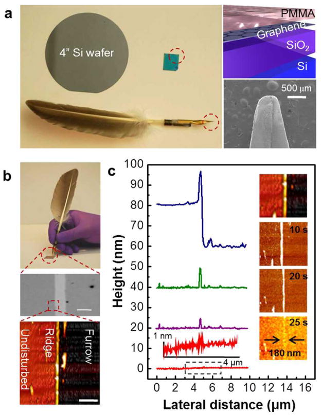
To probe the general behavior and properties of plow and ridge nanofabrication, we explored the use of a quill pen with a ~500 μm tip diameter to fabricate graphene nanostructures (Figure 1a). In this experiment, the quill pen was used by hand to generate a single line on a graphene-coated Si wafer that had been spin-coated with PMMA (Figure 1b). As expected, the ~400 μm width of the resulting line (Figure 1b) is commensurate with the tip diameter. Significantly, a ridge between the patterned and unpatterned areas was formed due to the lateral flow of PMMA during the writing process (Figure 1b). This ridge, which is 17 ± 2 nm high and 220 ± 24 nm wide, is significantly smaller than the pen diameter. Importantly, this ridge feature can be used as an etch mask to pattern the underlying graphene by exposing the sample to an oxygen/argon plasma (see Experimental Section), which anisotropically etches the PMMA and transfers the ridge pattern into the underlying substrate. After etching the sample for 20 s, only the PMMA ridge region remained (Figure 1c). This remnant ridge region can serve as an etch mask, and indeed, 5 s of subsequent reactive ion etching (RIE) processing resulted in the removal of the exposed graphene and most of the PMMA ridge, yielding a graphene ribbon with dimensions comparable to the original ridge. Residual PMMA was removed by rinsing the sample in acetone and subsequently annealing in shielding gas (5% H2, 95% Ar, 275 sccm) at 350 °C for 2 hours. AFM was used to image the final structure, revealing a 180 ± 22 nm wide graphene line, a dimension comparable to, but slightly smaller than, the 220 nm initial width of the PMMA ridge region (Figure 1c and Supporting Information). Note that Raman spectroscopic mapping of the substrate confirms the presence of graphene in the line region, and its absence elsewhere (see Supporting Information). These results point to the effectiveness of using the PMMA ridge as a mask layer for anisotropic etching and highlight the potential of plow and ridge nanofabrication to generate features that are significantly smaller than the size of the writing tool.
Figure 1.
a) Quill pen with a tip diameter of 500 μm shown with a 4″ Si wafer for scale. The pen is used to write a line on a Si wafer chip on which graphene has been deposited and coated with 25 nm film of poly (methyl methacrylate) PMMA. b) Writing a line on the surface (top panel) results in a clear furrow (middle panel, scale bar: 500 μm). Atomic force microscope (AFM) image of the edge of the furrow depicting the undisturbed region, the furrow, and the ridge between them (bottom panel, scale bar: 1μm). c) Height profiles and corresponding AFM images of time evolution (as-written, 10 s etching, 20 s total etching, and 25 s total etching) of the surface under an anisotropic reactive ion etching (RIE) process. AFM images are 2 μm in width.
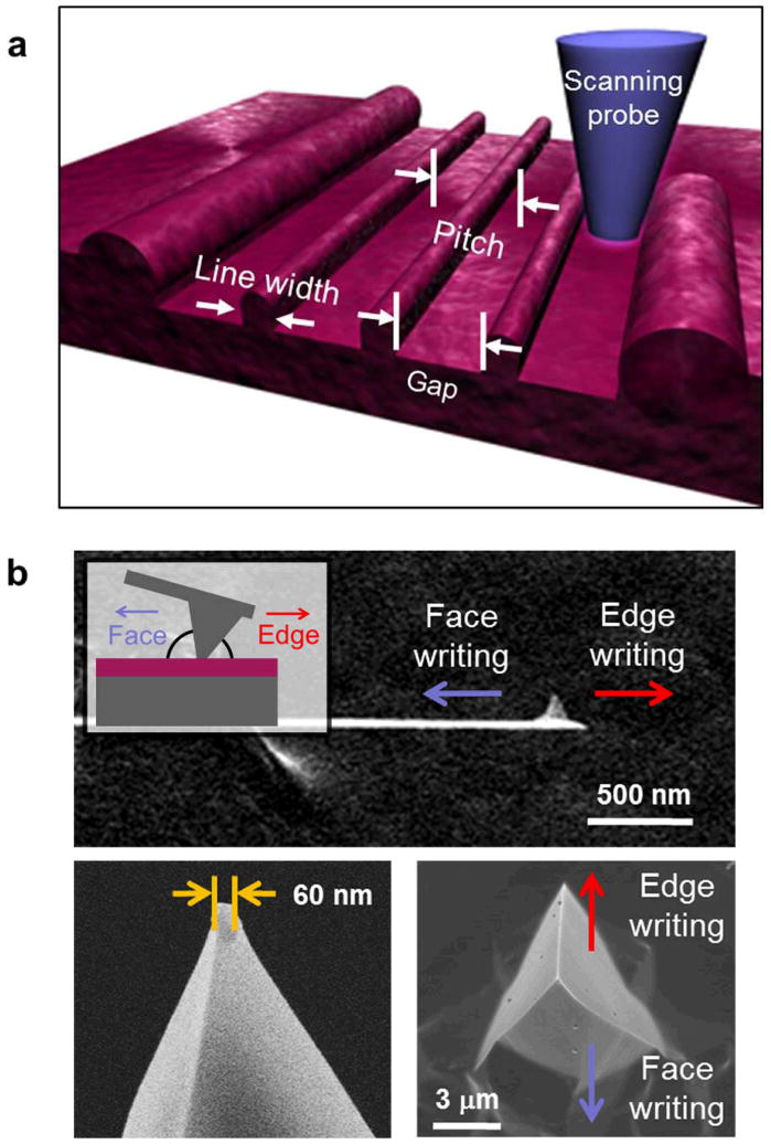
While the 2500:1 ratio between the 500 μm tip diameter of the quill pen and the patterned 180 nm graphene feature offers a dramatic demonstration of the concept of plow and ridge nanofabrication, the piezoelectric positioning, force feedback, and nanoscale tip sharpness used in AFM makes it a more powerful platform for studying this novel lithographic process. Indeed, one could envision an experiment in which an AFM probe is scanned across a PMMA-coated surface at a constant force in order to plow well-defined ridges (Figure 2a). However, as the geometry of the quill pen influenced the resulting plow and ridge pattern, it is important to consider the geometry of the AFM probe. For example, an AFM probe was characterized by scanning electron microscopy (SEM), and determined to have a diameter of ~60 nm and an asymmetric geometry that would likely yield different structures depending on the direction the tip was scanned (Figure 2b). Additionally, since cantilevers mounted in AFM systems typically are not parallel with the surface (often there is an engineered ~15° offset, Figure 2b), the direction of the scan, combined with the asymmetry of the tip are expected to significantly affect the type of pattern generated by plow and ridge nanofabrication.
Figure 2.
a) Schematic illustration of writing with a scanning probe tip on a polymer surface. b) Scanning electron microscopy (SEM) images of a commercial Si AFM probe. Edge- and face-first writing directions are defined based on the direction of tip movement. The inset schematic illustrates the geometric difference between edge- and face-directed writing.
In order to explore ridge formation systematically, we defined the two directions studied as the edge- and face-directions (Figure 2b). Since the tip was a triangular pyramid, scanning in the edge direction involved scanning with the sharp edge formed at the interface between two pyramidal faces, while scanning in the face-direction refers to the situation where the tip plows through the PMMA with one of the broad faces of the pyramid leading the way.
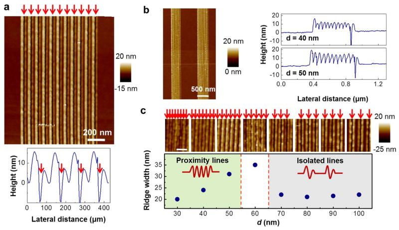
In a typical AFM experiment, a probe was mounted in an AFM and brought into contact with a Si wafer that had been spin-coated with 25 nm of PMMA. The tip was then scanned at a constant speed of 0.5 μm/s and held in contact with a constant force of 300 nN. PMMA was not baked after spin-coating to preserve its viscoelasticity.[9] Initially, scanning in the edge-direction was used to create a series of lines with a pitch d of 100 nm, which formed ridges in the sample as anticipated (Figure 3a). These ridges were ~15 nm in height, which is comparable to the 25 nm thickness of the PMMA film. Importantly, a consistent asymmetry is observed between the ridges formed on each side of a line (Figure 3a), which is attributed to uneven loading of the tip onto the AFM tip holder. This asymmetry makes the width of the ridges created by isolated lines difficult to control. By decreasing d, however, the ridge width was controlled, an effect we studied by varying d from 40 to 100 nm. For all lines written, ridges were formed that were ~15 nm high with uniform widths (Figure 3b and Supporting Information). For lines where d was between 70 and 100 nm, two ridges that were isolated from neighbouring lines were formed (Figure 3c). However, for d ≤60 nm, ridges from neighbouring lines begin to overlap, resulting in a type of constructive interference (see Supporting Information). We refer to this situation as the proximity regime. Subsequent experiments with decreasing d thus generated symmetric and homogenous ridges with uniform widths. Moreover, further reduction of d enabled control over the ridge width down to 25 nm (Figure 3c).
Figure 3.
a) AFM topographical image of edge-first writing on PMMA using an applied force F = 300 nN and a line pitch d = 100 nm. The bottom image shows the height profiles of ridge patterns. b) AFM topographical images and height profile of edge scratches (F = 300 nN, d = 40, and 50 nm) on the PMMA surface. c) AFM images of controlled ridge patterns written with d varied between 40 nm on the left to 100 nm on the right, the scale bar is 120 nm. The ridge width measured in each image is shown in the figure below where a transition from an isolated to a proximity regime is evident.
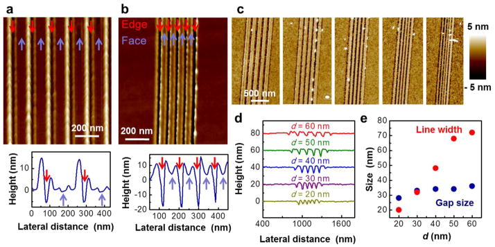
Having demonstrated that edge-first writing can yield defined features, we explored the potential for this technique to generate a wider range of features through the combination of edge-first and face-first writing. By alternatively writing lines face-first and edge-first with d = 100 nm, the ridge profiles of each writing direction were studied independently in the isolated regime. The ridges formed by face-first writing were significantly shorter than those formed by edge-first writing (Figure 4a), likely due to the difference in geometry and asymmetry imposed by the cantilever tilt. In contrast to the isolated regime, lines written while alternating between moving in the edge- and face-first directions with d = 40 nm generated ridges in the proximity regime wherein the ridges of neighbouring lines overlap (Figure 4b). Proximity ridges created using a combination of edge- and face-first lines have an advantage over proximity lines created by edge-first writing alone as the merging of dissimilar ridges yielded greater variation in ridge width and height. As a result, so called combination writing not only generated smaller features, but also yielded larger ones that could not be prepared by edge-first writing alone. For instance, varying d afforded greater control over the width of the ridges (see Supporting Information).
Figure 4.

AFM topographical images and line cuts of ridges written on PMMA with (a) d = 100 nm and (b) d = 40 nm, both with F = 300 nN. c) AFM images of patterned Si surfaces with d = 60, 50, 40, 30, and 20 nm (from left to right). d) Height profiles of surfaces shown in (c). e) Si line width and the size of the gap between lines at various values of d.
To demonstrate that this patterning procedure could be used to transfer patterns onto the underlying surface, RIE of the PMMA structures created by plow and ridge nanofabrication was employed. The sizes of the PMMA ridge and resultant Si pattern was monitored ex situ at different time points during etching (see Supporting Information). In an initial experiment with d = 60 nm, after 30 s of Ar/O2 plasma etching, only PMMA corresponding to the ridge region is left on the Si surface, which then served as a mask for subsequent anisotropic Si etching. In this case, an SF6/O2 plasma was used as an anisotropic etch selective for Si. Following the RIE processing, the sample was rinsed with acetone to remove PMMA residue.
In a series of experiments in which alternating face- and edge-first lines were written with varying d, the resultant ridge structures were used to generate Si lines that were as narrow as 20 ± 3 nm (Figures 4d and e), commensurate with the 23 ± 3 nm width of the original ridges. Importantly, the Si features were narrower than the 60 nm diameter of the scanning probe tip. It is noteworthy that by controlling d, we intentionally varied the ultimate feature size, while the gaps between ridges barely changed (Figure 4e) because the separation of the final features is primarily determined by the tip diameter.
We have described a unique approach for nanofabrication which utilizes a scanning probe as a plow on a polymer-coated surface to generate ridges that can serve as narrow etch masks. This technique was used to write patterns in Si and graphene, and in principle can be applied to the pattering of many other materials. Additional materials generality can be achieved by transferring the polymer pattern to a further etch mask with greater etch resistance. Unlike mask-based nanofabrication techniques such as nanoimprint lithography[10] or micro contact printing[11], plow and ridge nanofabrication is based on a serial writing process, which could be suitable for rapid prototyping applications. Additionally, this method in principle could be performed in a massively parallel fashion using cantilever-free scanning probe arrays such as those used in hard-tip, soft-spring lithography[6] with an appropriately tuned spring constant[12]. Moving forward, this technique would benefit from further investigation of the parameters that affect ridge formation such as temperature, scan speed, polymer properties, and tip geometry. Such studies could allow for the expansion and full exploitation of the capabilities of this technique. Given the ability of plow and ridge nanofabrication to overcome the resolution limit imposed by the tip diameter on conventional scanning probe lithography, we believe that it can be useful for many applications where making sub-20 nm nanowires or ribbons is important.
Experimental Section
AFM-based writing on PMMA
PMMA polymer (495 PMMA A2, MicroChem) was mixed with thinner solvent (A Thinner, MicroChem) in the ratio of 1:2 w/w. The diluted PMMA solution was spin-coated onto graphene-coated (single-layer graphene - Graphene Laboratories Inc.) and bare silicon surfaces at 500 rpm for 10 s with a ramping rate of 100 rpm/s followed by 2,000 rpm for 60 s with a ramping rate of 1000 rpm/s. The polymer-coated sample was not baked and the measured thickness of the PMMA is ~25 nm. Contact-mode AFM-based writing was performed in a DPN 5000 (NanoInk) under constant force conditions. First, Si probes (PPP-CONTR-W, Nanoworld AG) were calibrated by measuring force-distance curves followed by thermal tuning to determine the deflection sensitivity and spring constant (0.25 N/m typical) in a Bruker Dimension Icon AFM. After the spring constant of each probe was measured, they were then mounted in a DPN 5000 nanolithography system for patterning experiments. Next, the deflection sensitivity (250 nm/V typical) of the probes was found in the patterning instrument by taking three force-distance curves and finding the average slope of the contact line. The deflection set-point during patterning was specified based on the measured spring constant and deflection sensitivity in order to apply a constant force during writing. Experiments were performed at room temperature (22 °C) in ~33% relative humidity. The reactive ion etching (RIE) processes used for the Si and graphene substrates were selected for maximum selectivity for the material of interest. Reactive ion etching of PMMA and graphene was performed in a Samco RIE-10NR utilizing gas flow rates of 10 sccm O2 and 40 sccm Ar at a pressure of 4 Pa and a power of 30 W. Reactive ion etching of Si utilized gas flow rates of 10 sccm SF6 and 4 sccm O2 at pressure of 4 Pa and a power of 40 W.
Supplementary Material
Acknowledgments
This material is based upon work supported DARPA/MTO Award N66001-08-1-2044, AOARD Award FA2386-10-1-4065, AFOSR Awards FA9550-12-1-0280 and FA9550-12-1-0141, NSF Awards DBI-1152139 and DMB-1124131, DoD/NPS/NSSEF Fellowship Awards N00244-09-1-0012 and N00244-09-1-0071, Chicago Biomedical Consortium with support from Searle Funds at The Chicago Community Trust, and CCNE initiative of NIH Award U54 CA151880. K.A.B. and X.L. gratefully acknowledge support from Northwestern University’s International Institute for Nanotechnology.
Footnotes
Supporting Information is available on the WWW under http://www.small-journal.com or from the author.
Contributor Information
Dr. Wooyoung Shim, Department of Materials Science and Engineering, Northwestern University, 2220 Campus Drive, Evanston, IL 60208, USA
Dr. Keith A. Brown, Department of Chemistry, Northwestern University, 2145 Sheridan Road, Evanston, IL 60208, USA
Dr. Xiaozhu Zhou, Department of Chemistry, Northwestern University, 2145 Sheridan Road, Evanston, IL 60208, USA. School of Materials Science and Engineering, Nanyang Technical University, 50 Nanyang Avenue, Singapore 639798, Singapore
Boris Rasin, Department of Materials Science and Engineering, Northwestern University, 2220 Campus Drive, Evanston, IL 60208, USA.
Xing Liao, Department of Materials Science and Engineering, Northwestern University, 2220 Campus Drive, Evanston, IL 60208, USA.
Abrin L. Schmucker, Department of Chemistry, Northwestern University, 2145 Sheridan Road, Evanston, IL 60208, USA
Prof. Chad A. Mirkin, Email: chadnano@northwestern.edu, Department of Materials Science and Engineering, Northwestern University, 2220 Campus Drive, Evanston, IL 60208, USA. Department of Chemistry, Northwestern University, 2145 Sheridan Road, Evanston, IL 60208, USA
References
- 1.a) Xu S, Miller S, Laibinis PE, Liu G. Langmuir. 1999;15:7244–7251. [Google Scholar]; b) Rosa LG, Liang J. J Phys Condens Matter. 2009;21:483001. doi: 10.1088/0953-8984/21/48/483001. [DOI] [PubMed] [Google Scholar]
- 2.a) Snow ES, Campbell PM. Appl Phys Lett. 1994;64:1932–1934. [Google Scholar]; b) Science. 1995;270:1639–1641. [Google Scholar]
- 3.a) Kim Y, Lieber CM. Science. 1992;257:375–377. doi: 10.1126/science.257.5068.375. [DOI] [PubMed] [Google Scholar]; b) Tseng AA. Small. 2011;7:3409–3427. doi: 10.1002/smll.201100486. [DOI] [PubMed] [Google Scholar]
- 4.a) Piner RD, Zhu J, Xu F, Hong SH, Mirkin CA. Science. 1999;283:661–663. doi: 10.1126/science.283.5402.661. [DOI] [PubMed] [Google Scholar]; b) Ginger DS, Zhang H, Mirkin CA. Angew Chem, Int Ed. 2003;43:30–45. doi: 10.1002/anie.200300608. [DOI] [PubMed] [Google Scholar]; c) Salaita K, Wang Y, Mirkin CA. Nat Nanotech. 2007;2:145–155. doi: 10.1038/nnano.2007.39. [DOI] [PubMed] [Google Scholar]
- 5.Huo F, Zheng Z, Zheng G, Giam LR, Zhang H, Mirkin CA. Science. 2008;321:1658–1660. doi: 10.1126/science.1162193. [DOI] [PMC free article] [PubMed] [Google Scholar]
- 6.Shim W, Braunschweig AB, Liao X, Chai J, Lim JK, Zheng G, Mirkin CA. Nature. 2011;469:516–520. doi: 10.1038/nature09697. [DOI] [PubMed] [Google Scholar]
- 7.a) Braunschweig AB, Huo F, Mirkin CA, Nat CA. Chem. 2009;1:353–358. doi: 10.1038/nchem.258. [DOI] [PMC free article] [PubMed] [Google Scholar]; b) Giam LR, Mirkin CA. Angew Chem Int Ed. 2011;50:7482–7485. doi: 10.1002/anie.201100839. [DOI] [PubMed] [Google Scholar]
- 8.a) Briscoe BJ, Evans PD, Biswas SK, Sinha SK. Tribol Int. 1996;29:93–104. [Google Scholar]; b) Randall NX, Julia-Schmutz C, Soro JM. Surf Coat Tech. 1998;108–109:489–495. [Google Scholar]; c) Adams MJ, Allan A, Briscoe BJ, Doyle PJ, Gorman DM, Johnson SA. Wear. 2001;251:1579–1583. [Google Scholar]; d) Heyde M, Rademann K, Cappella B, Geuss M, Sturm H, Spangenberg T, Niehus H. Rev Sci Instrum. 2001;72:136–141. [Google Scholar]; e) Chen X, Vlassak JJ. J Mater Res. 2001;16:2974–2982. [Google Scholar]; f) Semaltianos NG. Microelectron J. 2007;38:754–761. [Google Scholar]
- 9.Sohn LL, Willett RL. Appl Phys Lett. 1995;67:1552–1554. [Google Scholar]
- 10.Chou SY, Krauss PR, Renstrom PJ. J Vac Sci Technol, B. 1996;14:4129–4133. [Google Scholar]
- 11.Xia Y, Whitesides GM. Annu Rev Mater Sci. 1998;28:153–184. [Google Scholar]
- 12.Eichelsdoerfer DJ, Brown KA, Boya R, Shim W, Mirkin CA. Nano Lett. 2013 doi: 10.1021/nl304268u. [DOI] [PubMed] [Google Scholar]
Associated Data
This section collects any data citations, data availability statements, or supplementary materials included in this article.


