Abstract
The high-quality and low-cost of the graphene preparation method decide whether graphene is put into the applications finally. Enormous efforts have been devoted to understand and optimize the CVD process of graphene over various d-block transition metals (e.g. Cu, Ni and Pt). Here we report the growth of uniform high-quality single-layer, single-crystalline graphene flakes and their continuous films over p-block elements (e.g. Ga) liquid films using ambient-pressure chemical vapor deposition. The graphene shows high crystalline quality with electron mobility reaching levels as high as 7400 cm2 V−1s−1 under ambient conditions. Our employed growth strategy is ultra-low-loss. Only trace amounts of Ga are consumed in the production and transfer of the graphene and expensive film deposition or vacuum systems are not needed. We believe that our research will open up new territory in the field of graphene growth and thus promote its practical application.
The fabrication of graphene over metals by chemical vapor deposition (CVD) is one of the most popular synthesis routes for this material. The reasons for this include the potential to scale-up the technique and a relatively low manufacturing cost. The CVD production of sp2 carbon entails passing a carbon feedstock over the surface of a catalyst substrate (e.g. a transition metal) at elevated temperatures. The catalyst then catalytically decomposes the feedstock to provide a carbon supply. The catalytic potential of transition metals is well established and is argued to arise from the partially filled d orbitals or by the formation of intermediate compounds which can absorb and activate the reacting medium. In short, the metals provide low energy pathways for reactions by changing oxidation states easily or through the formation of intermediates1. Researchers are also devoting efforts for the synthetic manufacture of graphene by CVD over non-metals, for example, hexagonal boron nitride and silicon oxide. However, these alternative substrates tend to exhibit low catalyst efficiency and progress is slow as compared to metal catalyst systems. Thus far, group VIII metals (Fe2 and Ru3), group IX metals (Co4, Rh5, and Ir6), group X metals (Ni7, Pd8 and Pt9), group XI metals (Cu10 and Au11) and alloys (Mo-Ni12, Cu-Ni13) have been shown as good substrates for graphene growth. The choice of catalytic substrate affects the growth behavior and the structure of graphene, including the nucleation density, layer number, size distribution, and crystallinity. In particular, low-pressure growth on Cu foils has attracted great interest for the fabrication of large-area single-layer graphene10. Recently, single-walled carbon nanotubes were demonstrated to growth from liquid Ga and In droplets on silicon substrates14. In 2013, few layer graphene films were found on the surface of a macroscopic molten Ga ball15. Compared with well studied d-block transition metals, p-block elements, the highest energy electron occupies a p-orbital are a virgin territory with respect to graphene growth.
It is widely accepted that an inhomogeneous nucleation density and the growth behavior of graphene over the catalyst surface are the primary causes for large area graphene consisting of randomly oriented and small graphene grains (typically in the range of 1–10 μm)16. This leads to a dramatic degradation of its electronic properties compared with those of pristine graphene and so is undesired17. Generally speaking, graphene nucleation preferentially occurs at high-surface energy locations such as grain boundaries or defects associated with a solid polycrystalline metal catalyst surface. Recently, Geng et al. reported the synthesis of hexagonal graphene flakes and continuous graphene films on liquid Cu surfaces. This is a particularly effective way to control the nucleation process because it eliminates the presence of grain boundaries in the substrate18.
The further development of graphene films in commercial applications will require a reproducible and cheap approach to synthesize high-quality graphene at ambient pressure and low temperature. Solid Cu as a catalyst was argued to self-limit the number of graphene layers forming to one, however in practice low pressure is required to obtain large area thickness uniformity and even then the number of layers varies between 1 and 319. Moreover, the high cost for growth catalysts, including expensive single crystal20, noble metal21 and film deposition processes12 will restrict their use for large area synthetic graphene and its commercial applications. In addition, most of the reported CVD graphene growth methods involve the etching of costly metal foils during transfer.
Here we report the growth of uniform single-layer, single-crystalline graphene on liquid p-block elements by atmospheric pressure CVD (APCVD). We easily transfer the graphene to arbitrary substrates by etching the trace liquid metal in dilute hydrochloric acid, which does not damage the graphene, or even the liquid-metal-supporting substrates. Our employed growth strategy is the ultra-low-loss of the substrate and minimal to no damage of the fabricated graphene. Our developed route does not require any film deposition or vacuum system. We believe that our research will open new pathways for large area and high quality graphene growth and as such promote its practical application.
Results
The growth of uniform single-layer graphene and its characterization
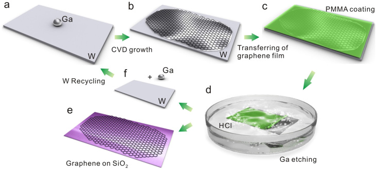
Ga was chosen as a model to demonstrate the catalytic ability of p-block elements for graphene fabrication. The approach for graphene grown over liquid Ga, which is supported by a W foil, is illustrated in Fig. 1. Briefly, a droplet of Ga (10 mg) was placed on W foil (50 μm thick, cut into 1×1 cm squares). Graphene growth was carried out at 1020°C under 300 sccm Ar, 0–30 sccm H2 and 5–20 sccm CH4 for 10–60 min in an APCVD system. The Ga spreads over the entire substrate by itself at elevated temperature after introducing CH4. After graphene growth, the graphene film was easily transferred onto arbitrary substrates by gently etching the Ga film in dilute hydrochloric acid, which not only does not damage the graphene, but also does not affect the Ga-supporting substrates (e.g. W). Thus, the W substrates can be used repeatedly as a support for liquid Ga to grow graphene. In effect, the employed growth strategy leads to ultra-low-loss of material, viz the only consumption for each growth cycle is a trace amount of Ga.
Figure 1. Schematic illustration of graphene growth over liquid Ga supported on a W substrate.
(a) A droplet of Ga is placed on a W support foil. (b) CVD growth of graphene on the liquid Ga surface. (c) The as-grown graphene is coated with a PMMA layer by a spin-coating process. (d) Graphene coated with PMMA is gradually separated from the W foil driven by H2 bubbles produced at the interface between the graphene and the Ga–W substrate. (e) Graphene transferred onto a SiO2/Si substrate. (f) The W foil can be reused as Ga-support.
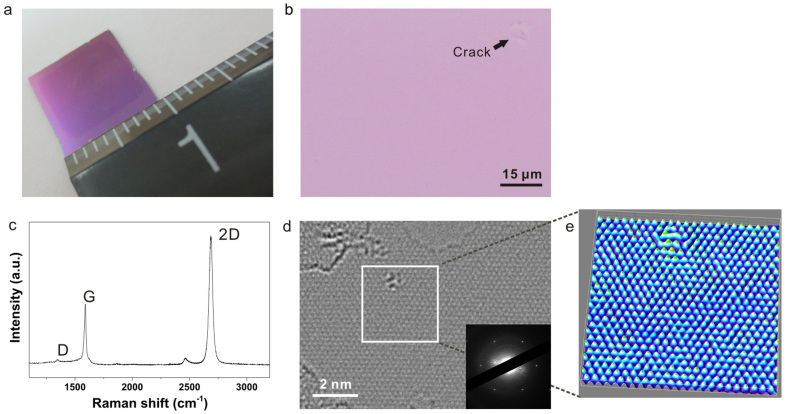
Fig. 2a shows a graphene film after transferring to a 300 nm SiO2/Si substrate. One can easily observe the graphene films due to the light interference effect22, which shows good uniformity of the graphene film on a macroscopic scale. An optical microscopy (OM) image in Fig. 2b further reveals the excellent uniformity of the graphene films. As compared to graphene grown on Cu, where the best obtained growth results in about 5% of graphene exceeds monolayer graphene, we obtain even better uniformity for graphene grown over Ga. The as-produced graphene was further examined by Raman spectroscopy (Fig. 2c), transmission electron microscopy (TEM), and selected-area electron diffraction (Fig. 2d–e). Raman spectroscopy is a non-destructive and powerful technique to identify the number of layers and presence of defects in graphene. The Raman 2D bands, which were collected over 300 sampling points on the transferred graphene, exhibited a symmetric single Lorentzian line shape with a full width at half-maximum of < 36.5 cm−1, the intensity ratio of G to 2D bands fell into a range of 0.4–0.5 and the intensity ratio of D to G bands < 0.05, which is characteristic for a monolayer graphene sheet with a relatively low defect density. Low voltage aberration-corrected, high-resolution transmission electron microscopy (LVAC-HRTEM) was employed to examine the microscopic structures of the obtained graphene. The HRTEM image in Fig. 2d and the corresponding selected-area electron diffraction (inset in Fig. 2d) highlights the six-fold symmetry single-crystal nature of the graphene. In Fig. 2e, a false 3D image from a Fourier enhanced TEM micrograph of the marked area in Fig. 2d highlights the perfect atom-scale crystal structure of the graphene. Based on the above characterization results and analysis, we demonstrate that large-area, high-quality and single-layer graphene can be grown on liquid Ga surfaces.
Figure 2. Graphene films transferred from Ga–W substrate.
(a) Graphene film transferred onto a SiO2/Si substrate. (b) Optical image of the transferred graphene on a SiO2/Si substrate. (c) Raman spectrum of the single-layer graphene. (d) HRTEM image and the selected-area electron diffraction pattern (inset) of the single-layer graphene. (e) A false 3D image originated from Fourier enhanced TEM micrograph of the marked area in Fig. 2d.
The domain shape of graphene grown on a liquid Ga surface
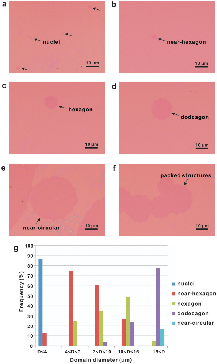
During the Ga-APCVD growth process, diverse crystal morphologies, including hexagons, dodecagons, near-circular shapes, closely packed structures, and continuous films were observed (Fig. 3). In general, the nucleation densities on Cu foils or Ni thin films are quite high, which leads to individual grain sizes being limited due to the crowding of graphene flakes. In other words, competitive growth exists among the domains, since adjacent nucleation sites restrict the further development of the domains. A liquid Ga surface completely eliminates the existence of grain boundaries and crystal defects. The atoms of liquid exhibit a characteristic readiness to flow, which in turn results in a more homogeneous surface and a low nucleation density as compared with the solid polycrystalline metal catalysts. As a comparison, the typical nucleation densities on liquid Ga and on solid polycrystalline Cu are about 1/1000 μm2 (Fig. 3a) and 1/10 μm2, respectively23,24,25. Recently, low nucleation density was obtained by sophisticated CVD process, including Cu pretreatments, electrochemical polishing, high-pressure annealing, and precise control of chamber pressure and partial pressure of carbon source26,27. One of the fascinating features of our strategy is that low nucleation density can be easily achieved though APCVD and excellent tolerance to variations in growth conditions. Therefore, the domain size for graphene grown over liquid Ga exceeds that found on Cu foil by a large margin. Subsequently grain growth of nuclei over liquid Ga tends to be uniform in all directions as can be seen by the formation of a dodecagon and near-circular shape (Fig. 3d, e) instead of four-fold graphene flakes, which generally occurs on Cu foils, possibly due to the anisotropic solid Cu lattice26. In order to identify any correlation between the graphene domain sizes and their shapes, the diameters of each domain were measured (Fig. 3g). The small dots were considered as nucleation densities, of which the diameters are mostly less than 4 μm. The diameters of hexagons and dodecagons mainly distribute in the range of 7–15 μm and 10–20 μm, respectively. The twelve-sided symmetric domains and near-circular domains are unique for the Ga-APCVD. This phenomenon may originate from the faster diffusion rate of carbon atoms on a liquid Ga surface than for solid polycrystalline metal films. In addition, liquid Ga provides a smooth surface without grain boundaries, and facilitates the growth of near circular shape domain in order to maintain a minimum surface energy. Most graphene domains will continue to grow until they are restricted by adjacent domains and so form a continuous film (Fig. 3e, f).
Figure 3. The domain shape of graphene transferred onto Si/SiO2 substrates.
(a) the nuclei of graphene transformed into (b) near-hexagons, then (c) hexagons, (d) dodecagons, and finally (e) near-circular and (f) closely packed structures. (g) Histogram plots of the size distribution of graphene domains for the different shapes.
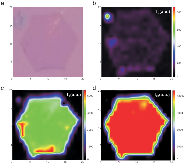
Fig. 4a shows a representative optical image of a hexagonal graphene flake grown on Ga. The intensity mapping of the characteristic graphene Raman peaks, D (≈ 1342 cm−1), G (≈ 1590 cm−1), and 2D (≈ 2687 cm−1) bands are plotted in Figure 3b–d for the hexagonally shaped single layer graphene grain. The typical intensity ratio (I2D/IG) within a grain is larger than 2, indicating that the samples are single-layer graphene28. Moreover, the intensity of the D band (ID) is negligible within the grain. Based on the Raman mapping of ID, grain boundaries do not appear to exist inside the grain, indicating the single crystal nature of these hexagonal graphene grains16.
Figure 4. Raman mappings of a single crystal graphene grain after transfer.
(a) Optical image of the graphene sample on a SiO2/Si substrate. (b–d) Intensity mappings of the D, G and 2D Raman peaks respectively, for a single crystal graphene grain. The spatial and spectral resolutions of the measurements are 1 μm and 1 cm−1 respectively.
The Nondestructive transfer of graphene and recycling of the W substrate
Most of the reported CVD graphene growth methods involve etching entire costly metal foils during the transfer process10. As shown at Fig. 1d–e, we easily transfer the graphene to arbitrary substrates by dissolving away the trace liquid metal (< 10 mg) in dilute hydrochloric acid. Moreover, the graphene coated by PMMA is helped to be released as a result of the formation of H2 bubbles at the interface between the graphene and the Ga-supporting substrates (e. g. W foils). The transfer process neither damages the graphene or the W substrates as supported by X-ray photoelectron spectroscopy (XPS) (Fig. 5c). No new peaks or peak shift can be observed between new W substrates and recycled ones. More importantly no difference in the quality or lateral size of the as-grown graphene could be observed when using pristine or recycled W substrates (Fig. 5a). Indeed the quality of graphene formed using a recycled W substrate was examined by Raman spectroscopy (see Fig. 5b). The intensity ratio of G to 2D bands was 0.48 and the intensity ratio of D to G bands was 0.08, and the full width at half-maximum (FWHM) was 38.4 cm−1, and these values are very similar to those presented in Fig. 2c. In short, recycling W substrates does not degrade the as-produced graphene quality.
Figure 5. Graphene grown on Ga/reused W substrate.
(a) Optical image of the graphene transferred onto a SiO2/Si substrate. (b) Raman spectra of the single-layer graphene. (c) XPS analysis of the new W substrate and the reused W substrate.
Discussion
Gallium, a carbon-insoluble metal is an excellent absorber of carbon29 and exhibits excellent catalytic ability for single-layer graphene growth under various experimental conditions. With many catalysts, for example Ni, an excessive carbon supply results in the formation of thick-layered graphene and even deposition of amorphous carbon on some transition metals7. However in the case of Ga, we always obtained uniform single-layer graphene even when the carbon supply was increased by over twenty-four times the minimum amount required to fully cover the surface with single layer graphene. No evidence for the presence of multilayer graphene was observed using high-resolution optical microscopy (Supplementary Fig. S2 and Table S1). This can be explained by the high surface energy of liquid gallium's surface. In order to lower its surface energy, Ga grabs and stores carbon atoms or clusters on its surface. During growth, surface bound carbon species nucleate and form a graphene film. Once the surface of Ga is fully covered by graphene, additional carbon atoms are blocked from the Ga surface and so further growth does not occur. In short, it is a self-terminating process. In addition, the high mobility of liquid Ga atoms may remove nucleation vacancies, preventing growth of a second layer at the same nucleation site. When the thickness of liquid Ga film increased by around three times the minimum required to fully cover the W substrate, no obvious changes were observed in the thickness and quality of the grown graphene (Supplementary Fig. S2 and Table S1). The role of hydrogen in the CVD growth of graphene over Cu foils has been demonstrated to affect the formation of active carbon species (CyHx)s required for graphene growth30. The morphology and size of the graphene domains, as well as the number of layers, change with hydrogen pressure. However, we found the thickness and the morphology of graphene on liquid Ga remained the same with or without the presence of hydrogen (Supplementary Fig. S2 and Table S1). Indeed, the growth window for homogeneous single-layer graphene growth over liquid Ga is large. This is undoubtedly an important advantage for practical applications as compared to most other conventional CVD routes for synthetic graphene. Our observations under various experimental conditions suggest that graphene growth on Ga at atmospheric pressure is self-limited, similar to what is argued for graphene grown over Cu using low-pressure CVD (LPCVD)10. It is widely accepted that the kinetics of the LPCVD is dominated by the surface reaction on the Cu foils, in other words, the process is surface reaction limited. Graphene synthesis by the APCVD process is known to have a kinetic rate-limiting step in the transport of gas molecules from the bulk to the surface19. Therefore, since growth is not self-limiting, any excess carbon supply would lead to the formation of multilayer graphene. For our Ga-APCVD process, the nature of liquid metal atoms with high mobility favors a higher carbon species diffusion rate. This means in our Ga-APCVD process, the dominant kinetic barrier is converted from the mass transport of carbon species to the surface reaction such as the methane decomposition process. In short, the homogeneous growth of high quality single-layer graphene on Ga arises due to the low solubility of carbon in Ga and high diffusion rate on liquid surfaces.
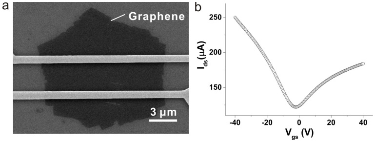
The high quality of the single-layer graphene grown on Ga was confirmed through electrical transport measurements. Back-gate field effect transistors were fabricated on 300-nm SiO2/p-Si substrates using conventional electron beam lithography. The source and drain electrodes were deposited using Ti/Au (5/45 nm) with a separation of 4 μm (Fig. 6a). Figure 6b demonstrates the highly reproducible transfer characteristics (Ids-Vgs) of the field effect transistors that were measured under ambient conditions. The V-shaped ambipolar property is typical for single-layer graphene with a zero bandgap. The extracted carrier mobility of electrons for this device is 7400 cm2 V−1s−1, which is significantly larger than the single-crystal graphene grown from Cu-LPCVD (~4000 cm2 V−1s−1)26 and liquid Cu surface (1000–2500 cm2 V−1s−1)18. We believe that the remarkable high mobility of the single-layer synthetic graphene grown over Ga benefits from the characteristic of Ga, which is notable for having one of the largest liquid ranges (from ~ 30 to ~ 2204°C) for a metal, and moreover has a low vapor pressure at elevated temperature. Unlike graphene growth over Cu foils in which Cu evaporates and redeposits during synthesis22, low vapor pressure of growth substrates provide a smooth surface, which is helpful for the formation of single-crystalline graphene under similar CVD growth conditions.
Figure 6. Electrical properties of single-layer graphene grown on Ga surface.
(a) A scanning electron microscopy image of the bottom-gated graphene field effect transistor (FET) made on a 300-nm SiO2/p-Si substrate using electron beam lithography followed by a metal (Ti/Pd/Au 0.5/30/20 nm) deposition. The scale bar is 3 μm. (b) The typical transfer characteristics of the fabricated graphene FETs under ambient conditions.
Our strategy for high quality synthetic graphene is not limited to the case of Ga over W. We prove the universality of our concept by growing graphene over In–W, Ga–Mo and In–Mo as can be seen in the supplementary information Fig. S3. Uniform single-layer graphene was obtained on In–W as confirmed by Raman characterization, which again demonstrates that p-block elements have the ability to catalytically grow uniform single-layer graphene. We also successfully grew high-quality, single-layer graphene on Ga–Mo systems at 900°C which provides hope for low temperature CVD growth using liquid main-group catalysts (see Supplementary information Table S2).
In summary, p-block elements are demonstrated as an attractive option for large high-quality graphene growth thus expanding the catalyst family for graphene grow beyond d-block transition metals. The electron mobility of single crystal domains grown on liquid Ga surfaces is as high as 7400 cm2 V−1s−1 under ambient conditions. Our employed growth strategy is ultra-low-loss. The only material consumption for each graphene growth run is a trace amount of Ga. Moreover, no film deposition or vacuum systems are required making the technique attractive not only from an economical stance but also from a practical perspectives. We believe that our research will open new pathways for environmentally and economically friendly large area and high-quality graphene growth.
Methods
Preparation of the substrates
The commercial Ga pellet was divided into small droplets in hot ethanol. A droplet of Ga (10 mg) was then placed on a W foil (50 μm, cut into 1×1 cm squares). Before loading gallium, the W foils were ultrasonicated and rinsed with acetone, ethanol and deionized water prior to being dried under a nitrogen stream. The Ga pellets had a purity of > 99.9999 wt.% and the W foils with a purity of > 99.95 wt.% were purchased from Alfa Aesar China (Tianjin) Co. Ltd. and Shanghai Minor Metals Co. Ltd.
CVD growth of graphene
The CVD growth of graphene was carried out in a quartz tube furnace (HTF 55322C Lindberg/Blue M) under ambient pressure. The growth protocol consisted of three steps: (1) heating the Ga-W substrates to 1020°C at a rate of 30–40°C/min under the flow of Ar and H2; (2) exposure of the substrates to a carbon source at 1020°C for 60 min under the flow of methane (CH4), Ar and H2; and (3) cooling the substrates to room temperature at a rate of 20°C/min under Ar, H2 and a reduced amount of CH4. The growth procedure is illustrated in Supplementary Figure S1.
Transferring the graphene to the target substrates
The process of transferring the graphene to the target substrates involves spin-coating a poly(methyl methacrylate) (PMMA) film onto the graphene-grown substrates and releasing the PMMA/graphene film by etching out Ga film in a diluted hydrogen chloride (1:1) for 1 h. This was followed by a rinse in ultrapure water to remove the metal ions. The PMMA layer was dissolved with hot acetone after the PMMA/graphene film was transferred onto the target substrates (e.g. SiO2/Si).
Characterization
Optical images were taken with an optical microscope (Olympus DX51, Olympus), and Raman spectroscopy was performed with a laser micro-Raman spectrometer (Renishaw inVia, Renishaw, 532 nm excitation wavelength). The TEM images were taken with an aberration-corrected, high-resolution TEM (AC-HRTEM, JEOL 2010F) operating at 80 kV with graphene samples directly transferred onto a copper grid. XPS was performed on Kratos Analytical, AXIS-Ultra using monochromatic Al Kα radiation (225 W, 15 mA, 15 kV). The current (I)–voltage (V) data were collected in the probe station under ambient conditions.
Author Contributions
L.F. developed the concept and conceived the experiments. J.W., M.H.R., H.T.X. and Z.S.L. carried out the experiments. L.F. and J.W. wrote the manuscript. L.F., J.W., M.Q.Z., L.F.T., B.Y.D., Y.D., S.W., L.M.P. and J.E. contributed to data analysis and scientific discussion.
Supplementary Material
Supporting information
Acknowledgments
The research was supported by The Sino-German Center for Research Promotion (Grants GZ 871) and the Ministry of Education (Grants 20120141110030). MHR thanks the EU (EFRE), the SAB and the SMWK. We thank Nicole Geiβler for her help about TEM characterization.
References
- Mattevi C., Kim H. & Chhowalla M. A review of chemical vapour deposition of graphene on copper. J. Mater. Chem. 21, 3324–3334 (2011). [Google Scholar]
- An H., Lee W. J. & Jung J. Graphene synthesis on Fe foil using thermal CVD. Curr. Appl. Phys. 11, S81–S85 (2011). [Google Scholar]
- Sutter E., Albrecht P. & Sutter P. Graphene growth on polycrystalline Ru thin films. Appl. Phys. Lett. 95, 133109 (2009). [Google Scholar]
- Ago H. et al. Epitaxial chemical vapor deposition growth of single-layer graphene over cobalt film crystallized on sapphire. ACS Nano 4, 7407–7414 (2010). [DOI] [PubMed] [Google Scholar]
- Liu M. X. et al. Thinning segregated graphene layers on high carbon solubility substrates of rhodium foils by tuning the quenching process. ACS Nano 6, 10581–10589 (2012). [DOI] [PubMed] [Google Scholar]
- Vo-Van C. et al. Epitaxial graphene prepared by chemical vapor deposition on single crystal thin iridium films on sapphire. Appl. Phys. Lett. 98, 181903 (2011). [Google Scholar]
- Reina A. et al. Large area, few-layer graphene films on arbitrary substrates by chemical vapor deposition. Nano Lett. 9, 30–35 (2009). [DOI] [PubMed] [Google Scholar]
- Kwon S. Y. et al. Growth of semiconducting graphene on palladium. Nano Lett. 9, 3985–3990 (2009). [DOI] [PubMed] [Google Scholar]
- Gao T. et al. Growth and atomic-scale characterizations of graphene on multifaceted textured Pt foils prepared by chemical vapor deposition. ACS Nano 5, 9194–9201 (2011). [DOI] [PubMed] [Google Scholar]
- Li X. S. et al. Large-area synthesis of high-quality and uniform graphene films on copper foils. Science 324, 1312–1314 (2009). [DOI] [PubMed] [Google Scholar]
- Oznuluer T. et al. Synthesis of graphene on gold. Appl. Phys. Lett. 98, 183101 (2011). [Google Scholar]
- Dai B. Y. et al. Rational design of a binary metal alloy for chemical vapour deposition growth of uniform single-layer graphene. Nat. Commun. 2, 522 (2011). [DOI] [PubMed] [Google Scholar]
- Liu X. et al. Segregation growth of graphene on cu-ni alloy for precise layer control. J. Phys. Chem. C 115, 11976–11982 (2011). [Google Scholar]
- Rao R., Eyink K. G. & Maruyama B. Single-walled carbon nanotube growth from liquid gallium and indium. Carbon 48, 3971–3973 (2010). [Google Scholar]
- Ding G. Q. et al. Chemical vapor deposition of graphene on liquid metal catalysts. Carbon 53, 321–326 (2013). [Google Scholar]
- Yu Q. K. et al. Control and characterization of individual grains and grain boundaries in graphene grown by chemical vapour deposition. Nat. Mater. 10, 443–449 (2011). [DOI] [PubMed] [Google Scholar]
- Yazyev O. V. & Louie S. G. Electronic transport in polycrystalline graphene. Nat. Mater. 9, 806–809 (2010). [DOI] [PubMed] [Google Scholar]
- Geng D. C. et al. Uniform hexagonal graphene flakes and films grown on liquid copper surface. P. Natl. Acad. Sci. USA 109, 7992–7996 (2012). [DOI] [PMC free article] [PubMed] [Google Scholar]
- Bhaviripudi S., Jia X. T., Dresselhaus M. S. & Kong J. Role of kinetic factors in chemical vapor deposition synthesis of uniform large area graphene using copper catalyst. Nano Lett. 10, 4128–4133 (2010). [DOI] [PubMed] [Google Scholar]
- Zhang Y. et al. Comparison of graphene growth on single-crystalline and polycrystalline Ni by chemical vapor deposition. J. Phys. Chem. Lett. 1, 3101–3107 (2010). [Google Scholar]
- Gao L. B. et al. Repeated growth and bubbling transfer of graphene with millimetre-size single-crystal grains using platinum. Nat. Commun. 3 (2012). [DOI] [PMC free article] [PubMed] [Google Scholar]
- Ismach A. et al. Direct chemical vapor deposition of graphene on dielectric surfaces. Nano Lett. 10, 1542–1548 (2010). [DOI] [PubMed] [Google Scholar]
- Robertson A. W. & Warner J. H. Hexagonal single crystal domains of few-layer graphene on copper foils. Nano Lett. 11, 1182–1189 (2011). [DOI] [PubMed] [Google Scholar]
- Duong D. L. et al. Probing graphene grain boundaries with optical microscopy. Nature 490, 235–240 (2012). [DOI] [PubMed] [Google Scholar]
- Tsen A. W. et al. Tailoring electrical transport across grain boundaries in polycrystalline graphene. Science 336, 1143–1146 (2012). [DOI] [PubMed] [Google Scholar]
- Li X. S. et al. Large-area graphene single crystals grown by low-pressure chemical vapor deposition of methane on copper. J. Am. Chem. Soc. 133, 2816–2819 (2011). [DOI] [PubMed] [Google Scholar]
- Yan Z. et al. Toward the synthesis of wafer-scale single-crystal graphene on copper foils. ACS Nano 6, 9110–9117 (2012). [DOI] [PubMed] [Google Scholar]
- Ferrari A. C. et al. Raman spectrum of graphene and graphene layers. Phys. Rev. Lett. 97, 187401 (2006). [DOI] [PubMed] [Google Scholar]
- Pan Z. W., Dai S., Beach D. B., Evans N. D. & Lowndes D. H. Gallium-mediated growth of multiwall carbon nanotubes. Appl. Phys. Lett. 82, 1947–1949 (2003). [Google Scholar]
- Vlassiouk I. et al. Role of hydrogen in chemical vapor deposition growth of large single-crystal graphene. ACS Nano 5, 6069–6076 (2011). [DOI] [PubMed] [Google Scholar]
Associated Data
This section collects any data citations, data availability statements, or supplementary materials included in this article.
Supplementary Materials
Supporting information


