Abstract
We fabricated ultrathin metal-semiconductor Schottky diodes for use as transmission particle detectors in the biological microbeam at Columbia University’s Radiological Research Accelerator Facility (RARAF). The RARAF microbeam can deliver a precise dose of ionizing radiation in cell nuclei with sub-micron precision. To ensure an accurate delivery of charged particles, the facility currently uses a commercial charged-particle detector placed after the sample. We present here a transmission detector that will be placed between the particle accelerator and the biological specimen, allowing the irradiation of samples that would otherwise block radiation from reaching a detector behind the sample. Four detectors were fabricated with co-planar gold and aluminum electrodes thermally evaporated onto etched n-type crystalline silicon substrates, with device thicknesses ranging from 8.5 μm – 13.5 μm. We show coincident detections and pulse-height distributions of charged particles in both the transmission detector and the commercial detector above it. Detections are demonstrated at a range of operating conditions, including incoming particle type, count rate, and beam location on the detectors. The 13.5 μm detector is shown to work best to detect 2.7 MeV protons (H+), and the 8.5 μm detector is shown to work best to detect 5.4 MeV alpha particles (4He++). The development of a transmission detector enables a range of new experiments to take place at RARAF on radiation-stopping samples such as thick tissues, targets that need immersion microscopy, and integrated microfluidic devices for handling larger quantities of cells and small organisms.
Keywords: Solid state detectors, low-energy charged particle detectors, Detector design and construction technologies and materials
1. Introduction/Background
The use of ionizing radiation microprobes for biological applications [1] has led to major advances in assessing intra- or inter-cellular biological responses to ionizing radiation, such as DNA damage in subnuclear targets [2], or bystander responses [3]. The advantage of single ion microprobes is their ability to deliver known doses in precise locations within a cell or population of cells. In the early 1990’s, the Radiological Research Accelerator Facility at Columbia University was one of the first facilities to build a single ion microbeam [4, 5], and today there are over 30 radiobiological microbeams globally [6].
Since a major advantage of a single-ion microprobe is the precise delivery of a known dose of radiation, an important component of any microbeam facility is the detection of the charged particles. Further, a particularly important feature of a detector is whether the particles are detected between the accelerator and the sample (transmission detection) or beyond the irradiated sample. A transmission detector is required when the target specimen would otherwise prevent radiation from reaching a detector mounted beyond the sample.
In order to highlight the importance of a transmission detector, we first consider particle energy deposition and absorption in section 1.1. Then we discuss how this energy deposition can be used for detection in section 1.2, and present the current state of the art of available detectors in section 1.3.
1.1 Particle range and energy deposition into an absorbing material
When heavy charged particles such as protons (H+) and alpha particles (4He++) pass through a material, they can have two types of interactions: Nuclear interactions (e.g. Rutherford scattering) between the nuclei of the particle and the material, and Coulombic interactions between the charged particle and the electrons in the absorbing material [7]. The dominant interaction with the particle energy in this work will be the Coulombic interaction.
The Coulombic interactions occur as excitation or ionization of the irradiated material. Either bound electrons are excited into a higher energy state (excitation), or are removed from the atom completely creating an electron/ion pair (ionization) in a gas, or an electron-hole pair in a semiconductor. The energy loss due to Coulombic interactions is called Linear Energy Transfer (LET), which is the linear rate of energy loss (dE/dx) of a charged particle due to ionization and excitation. The LET of a particle in an absorbing material follows the Bethe-Bloch Formula [7]:
Where v is the velocity of the particle, z is the charge of the particle, N is the number density of the absorber atoms, and Z is the atomic number of the absorber atoms, m0 is the particle’s rest mass, and e is the electronic charge. I is an experimentally determined parameter for each element representing the average excitation and ionization potential of the absorber.
The amount of energy, E, that is deposited by a particle with a certain energy, into a material with certain thickness, can be estimated using LET for thin materials and small changes in energy. However, once the particle starts losing energy, LET increases, resulting in an energy deposition following a Bragg curve [7]. The range of a particle can be simulated for multiple layers using SRIM (the Stopping and Range of Ions in Matter), a semi-empirical software that tabulates experimental LET values and performs simple Monte Carlo simulations for several layers of absorbing material [8]. Figure 1(a) shows the LET of hydrogen and helium particles in silicon as a function of particle energy, as calculated by SRIM. Figure 1(b) shows the range of these particles in silicon as a function of particle energy. For example, a 5 MeV alpha particle has an LET of 140 KeV/μm in silicon, or 90 KeV/μm in tissue. This particle has a range of just ~25 μm in silicon, or a range of ~35 μm in tissue, and therefore a transmission silicon detector must be much thinner than 25 μm to leave enough energy in the particle to reach the sample. While particles with such short ranges make the fabrication of a transmission detector difficult, the dose delivered to a cell nucleus by even a single alpha particle is biologically relevant [9].
Figure 1.
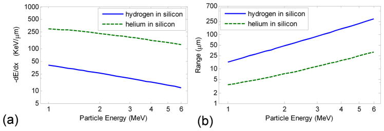
(a) LET, and (b) Range as a function of Particle Energy. Values obtained from SRIM.
Currently RARAF uses a 300 μm thick solid state detector (ORTEC model R-015-050-300, Oak Ridge, TN) [5]. With this thickness detector, incident alpha particles will deposit all their energy and will be stopped by the detector. This setup is limited to detection of radiation behind thin samples that do not stop alpha particles, such as cells or small organisms (e.g. C. Elegans) mounted on 3 μm polypropylene substrates, with very thin layers of medium. Thicker samples (e.g. tissues), thicker layers of medium, immersion microscopy, or microfluidic channels would stop the radiation, and require a transmission detector mounted prior to the sample. RARAF currently estimates dose rates in these situations by timed irradiations: assuming the beam rate is constant, the dose is calculated by the amount of time that the shutter is open. This is accurate with higher doses, but not accurate when interested in low doses (e.g. down to single particle irradiations) due to the Poisson distribution of the generated ions.
1.2 Detector physics
As mentioned in the previous section, incident radiation will cause ionization or electron-hole pair generation in the absorbing material. The average energy required to create an ion pair or electron-hole pair, ε, depends on the absorbing material, e.g. 3.62 eV for Silicon at room temperature or typically 15–30 eV in a gas detector [7, 10].
Therefore, the number of electron-hole pairs that are generated from a charged particle passing through a material will be equal to the energy deposited in that material (E) divided by the average energy required to generate an electron-hole pair (ε), or: n = E/ε. As an example, if a 5 MeV alpha particle deposits 1 MeV into a thin silicon layer, then 2.76e5 electron-hole pairs are created.
If the irradiated material is a rectifying junction (i.e. a diode) biased in the reverse direction, and the flow of leakage current is negligible, an electric field will form and deplete the material from intrinsic charge carriers (free electrons and holes) that are generated due to background sources (i.e. heat or light). If the charged particle passes through the depleted region, the newly generated charge carriers (electron-hole pairs) will be swept towards their respective electrodes (negative charges to the cathode, and positive charges to the anode), and can be detected as a pulse of current after amplification.
The rectifying junction can be created by dopants in a semiconductor (p-n or p-i-n diodes), or at the interface of a metal and a semiconductor (Schottky barriers). We developed Schottky diodes by depositing aluminum and gold electrodes onto silicon [11].
1.3 Detector applications
There are 3 technologies typically used for detection of radiation: semiconductor detectors, gas detectors and scintillators coupled to photon detectors [12]. Plastic scintillator sheets (10–50 μm thick BC400R) emit photons when hit with charged particles, and when coupled to photomultiplier tubes have been used as detectors in microbeam applications [13–15]. However, the energy resolution is poor; the typical energy required to produce 1 photoelectron is on the order of 1000 eV or more [7]. Gas detectors rely on the ionization of a gas (such as P10, 10% methane in argon), and have also been used as microbeam transmission detectors [13]. The average energy to create an ion pair in a gas is 15–30, roughly 5–10 times more than the materials used in semiconductor detectors, where the energy required to create an electron-hole pair in silicon is 3.62 eV. RARAF currently has a custom built gas counter that has an 8 mm long gas ionization chamber [5]. Commercial semiconductor detectors are available from companies such as ORTEC, and are reverse biased diodes that rely on the generation of electron-hole pairs by charged particles. The thinnest commercial detector currently offered by ORTEC is 100 μm.
All three technologies listed above have the same problem when being used as a transmission detector for alpha particles - they are usually too thick, and will block these high-LET particles from reaching the sample. As mentioned in section 1.1, the range of a 5MeV alpha particle is only ~25 μm in silicon, and these commercial products are typically not thin enough to be used as transmission detectors for these particles.
The current state of the art fabrication of “ultra thin” p-i-n diode detectors, which range from 4.5–22 μm, is shown in [10, 16, 17]. These devices are made from 380 μm, <100>, p-type silicon wafers, which are anisotropically etched with TMAH for 14 hrs. The detector diode is formed by phosphorous (n) doping to form a p-n junction, and aluminum is deposited on both sides for metal contacts. Initially developed as a ΔE-E telescope to measure energy and identity of particles in vacuum, the device was incorporated at the Lund Microprobe as a 9–11 μm thick transmission detector for cell irradiation [16].
At RARAF we pursued the creation of ultra-thin metal-semiconductor Schottky diodes as transmission detectors for alpha particles. This type of detector maintains the sensitivity of semiconductor detectors, which generate 5–10 times more electron-hole pairs per particle than gas detectors, and do not lose sensitivity by converting electrons to photons. Further, this type of diode does not require doping of the silicon, and therefore fabrication can be simpler and cheaper. The next section will describe the fabrication of our devices.
2. Materials and Methods
2.1 Fabrication
A crystalline silicon wafer with initial thickness 10 +/− 4 μm (Virginia Semiconductor, Fredericksburg, VA) was cleaved into approximately 10mm × 10mm squares. These wafer chiplets were suspended over a 6mm hole drilled into a glass slide, and glued permanently in place using a 50 μm layer of SU-8 2050 (Microchem, Newton MA).
A shadow masking procedure was used to deposit the 100nm co-planar gold and aluminum electrodes on the silicon substrate. A plastic film (PMMA, 100 μm thick) was cut to the approximate size and aligned manually to physically mask one half of the suspended wafer, and aluminum was thermally evaporated. A similar shadow mask was then used to cover the aluminum electrode and a small gap (~500 μm), and gold was evaporated onto the rest of the wafer.
The sample was then turned over and etched to different thicknesses using a SF6 plasma etching in an inductively coupled plasma reactive ion etcher (Oxford Instruments Plasmalab 80plus ICP-RIE, Concord MA). Only the area exposed by the hole in the glass slide was etched, leaving a locally thinned suspended membrane. We prepared 4 samples: etching for 10s, 30s, 60s, and 90s with 20 sccm of SF6 at 400W ICP power and 50W RF power. Conductive epoxy (Epotek H20E, Billerica MA) is then used to connect wires to the electrodes. Figure 2 shows the exploded view of our detector, and pictures of the fabricated device.
Figure 2.

exploded view of the detector (a), and images of top (b) and bottom (c) of detector
2.2 Experimental Setup
The detector is placed between the radiation source and a commercial detector above it. Figure 3 shows a 3D CAD drawing of the placement of the detector (a), and a 2D cutout view (b). The commercial detector is place 21.9 mm away from the radiation source and the transmission detectors are placed 1.1 mm away from the radiation source.
Figure 3.
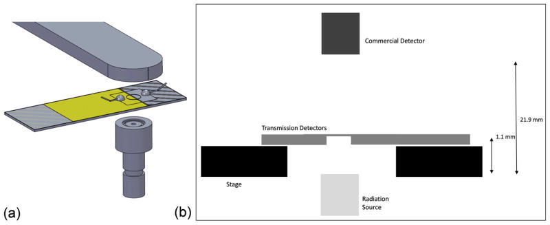
(a) placement of the transmission detector between a radiation source and the commercial absorption detector above it. (b) Cross-section view of the endstation and detector placement.
The output signals from both detectors are fed into charge sensitive preamplifiers (Canberra 2003BT, Meriden, CT). The preamplifier converts the charge into a voltage, with a sensitivity of 0.45V/pC. The output from the preamplifiers are fed into a shaping amplifier, with a rectangular filter, that yields a gaussian pulse after 100–1000x gain, and 1–10us shaping constants (ORTEC model 570, Oak Ridge, TN). Figure 3 shows the electronics used in the detection experimental setup.
After amplification, the pulses are read in two manners: oscilloscope traces of pulses as a function of time and analog to digital multiple channel analyzer (ADC-MCA) output, as shown in figure 4. The oscilloscope can be used to verify that both pulses from the transmission detector and the commercial detector are coincident. The ADC-MCA displays a distribution of pulse heights, where each channel of the ADC corresponds to a narrow bin of pulse voltage. Thousands of pulses can be registered, and the length of acquisition is recorded. Total counts are found by integrating beneath the distribution, and count rate is found by dividing the total counts by the acquisition time. We calibrated the ADC-MCA channel numbers to input voltage pulses and incoming particle energy using the test input of the Canberra preamplifier and a function generator.
Figure 4.

experimental setup: electronics used for detection
2.3 Thickness measurement
We use an energy loss measurement method similar to that described in [17] to determine the thickness of the etched samples. Briefly, we measure the energy of particles with and without passing through the etched samples, and estimate each sample’s thickness with SRIM calculations. In this section, we use 2.7 MeV protons (H+) incident on the commercial detector.
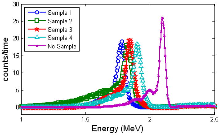
Figure 5 shows the energy deposited in the commercial detector with and without passing through our four detectors. The energy loss range for each of our samples was found to be 320 KeV, 270 KeV, 250 KeV and 195 KeV. We performed a range of SRIM calculations to estimate what the energy loss is using our geometry and multiple thicknesses of silicon. The layers used in the calculations were a 500nm silicon nitride window, 1.1 mm of air, 1–15 μm of silicon, and 20.9 mm of air. The energy loss after transmission across these layers was found for different incoming energies of protons and alpha particles. Using these SRIM calculations as a calibration, we estimate thicknesses of our wafers to be 13.5 μm, 11.5 μm, 11 μm, and 8.5 μm thick.
Figure 5.
Proton energy loss measurement to determine the thickness of the samples. Protons were detected in the commercial detector, with and without passing through our samples.
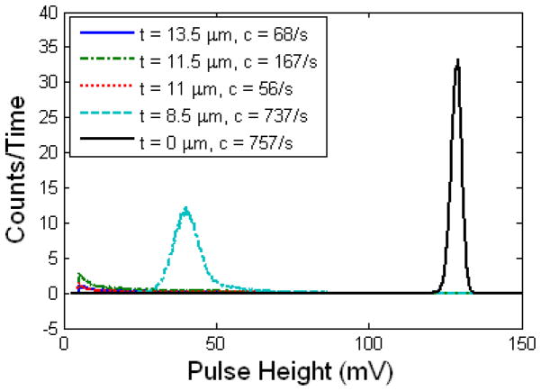
We performed the same experiment as above with alpha particles (helium nuclei) to ensure that high-LET particles can pass through our detectors. Figure 6 shows the distribution of pulses detected by the commercial detector from alpha particles with and without passing through our samples. The integral beneath the ADC-MCA distribution represents the count rate.
Figure 6.
ADC-MCA distribution of 5.4 MeV 4He++ particles through our samples. Measurements were taken from the commercial detector set up behind our transmission detector. t is the thickness of the sample between the radiation source and the commercial detector, and c is the count rate measured by the integral beneath these curves. It appears that these 4He++ particles only pass cleanly through the 8.5 μm sample.
It can be seen from figure 6 that only the thinnest detector allows the alpha particles to pass through with enough remaining energy to ensure that it reaches the commercial detector. Therefore in the following sections we characterize only the 8.5 μm detector for use with alpha particles, and characterize the 13.5 μm detector for use with protons.
3. Experiments
We performed 3 sets of experiments with our detectors. The first set of experiments is characterization of the fabricated devices to determine the thickness and electrical properties of the samples, and ensure that we indeed fabricated Schottky diodes (section 3.1). The second set of experiments tested the devices with alpha particles (section 3.2), and the third set of experiments tested the devices with protons (section 3.3).
3.1 Diode Characteristic Measurements: I-V curves and C-V curves
First, we verified that the devices behaved as Schottky diodes. To measure the I-V curves, we used a high voltage source measurement tool (Kiethley 237, Cleveland, OH). To measure the C-V curves, we used a parameter analyzer (Agilent 4155C) coupled to an inductance-capacitance-resistance (LCR) measurement tool (Agilent 4284A). An oscillating AC voltage of 25mV and 1kHz was added to a bias voltage ranging from −0.5V to 4V to measure capacitance via a phase shift.
The curves in figure 7 demonstrate that we have indeed fabricated diodes. Applying a positive voltage to the gold electrode causes current to flow, and when a negative voltage is applied, the Schottky barrier limits the flow of current to less than 20 μA. This rectifying junction is required to set up an electric field across the silicon detector, as discussed in section 1.1.
Figure 7.
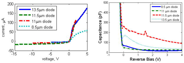
I-V curves and C-V curves of 4 diode samples to ensure they behave like diodes, and that current only flows in the forward direction. This allows an electric field to be set up when biased in the reverse direction.
3.2 Helium Nuclei (4He++) with the 8.5 μm detector
3.2.1 Simultaneous pulses from the transmission and commercial detectors
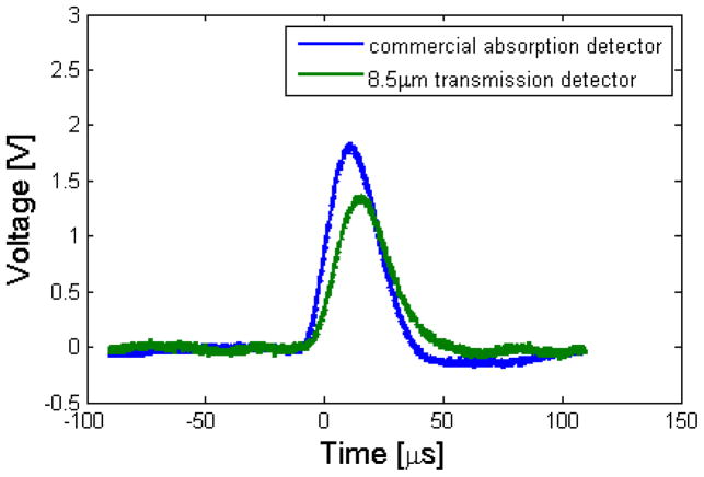
This section shows the simultaneous capture of oscilloscope (Tektronix TDS3052C, Beaverton, OR) traces from our detector and the commercial detector above it. Using helium nuclei from the RARAF microbeam, we show that a single particle causes a pulse in both detectors. The data collection was triggered on the commercial detector, and shown in figure 8.
Figure 8.
Oscilloscope trace of coincident pulses from the 8.5 μm transmission detector and the commercial absorption detector mounted behind it. These traces were taken with 40V bias at the center between electrodes, and triggered on the commercial detector.
Figure 8 shows a representative oscilloscope trace of the two detectors. The noise on the transmission detector channel is expected to be higher with our device than with the commercial device due to packaging and RF noise from unshielded wires compared to the packaged commercial detector. The difference in noise between the two devices was found to be minimal, and attributable to the signal-gathering electronics.
Ignoring relativistic effects, the kinetic energy of the alpha particle is equal to 1/2mV2, and a 5 MeV (8.01 e-13 Joule) alpha particle has a velocity of 1.55e7 m/s. This is 5% of the speed of light, so our assumption to ignore relativistic effects is valid. Given that the speed of the particle, and the detectors are 2cm away from each other, it is expected that the time between pulses should be 1.3 ns. Since the integration time of the signal is 10 μs, these pulses occur at essentially the same time, and any discrepancy is due to the electronics and signal gathering.
3.2.2 Traverse across 8.5 μm transmission detector
The next experiment we performed was to characterize the performance of the detector as a function of the location of the beam. Since the electrodes were defined by a wide shadow masking procedure, the diode is essentially a 1D structure, and we can traverse from one electrode to the other.
Figure 9 shows the location of the detector with respect to the beam. The right side of the figure shows the pattern that we used to traverse across the detector from the gold to the aluminum electrodes. The aluminum electrode is 720 μm away from the gold electrode.
Figure 9.
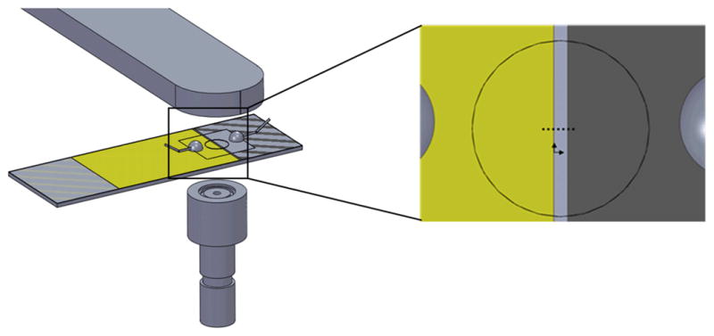
The beam was traversed across the detector perpendicular to the gold and aluminum electrodes. The gap between the electrodes is 720 μm, and measurements were taken at 150 μm intervals.
Figure 10(a) plots these distributions in pulse height as a function of distance away from the gold electrode edge, and Figure 10(b) plots the count rate as a function of this distance. It appears that the maximum pulse height increases as the beam gets closer to the aluminum edge, the distribution broadens, but the count rate stays essentially the same. Once the beam reaches the aluminum electrode, the count rate diminishes. It appears that there is no depletion region beneath the aluminum electrode.
Figure 10.
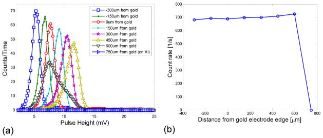
Traverse experimental results, showing distribution of pulses as a function of (a) distance from the gold electrode and (b) count rate at the same points. The aluminum electrode is 720 μm from the gold electrode. This experiment was done with 5.4MeV He and a 40V bias voltage.
3.2.3 Count Rate Analysis, 8.5 μm transmission detector
The MCA pulse height distribution from the transmission detector is plotted in Figure 11 along with the pulse distribution from the commercial detector behind it, and the commercial detector with nothing in the way. The count rate is found by integrating beneath these curves.
Figure 11.
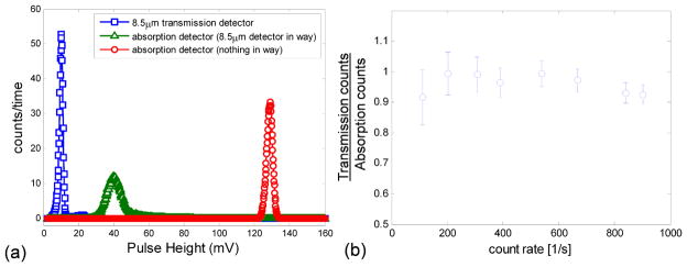
(left) ADC-MCA histograms of detections from the transmission detector and the absorption detector, with and without the transmission detector in the way. The count rate is 737, 757, and 734, respectively for the transmission detector, and the absorption detector with and without the transmission detector in the way. (right) Comparing the count rate from the 8.5 μm transmission detector and the commercial detector above it for multiple operating conditions. It appears that the count rates are within 10% for the transmission and absorption detector.
Figure 11(a) shows for a single operating condition that the count rate is the same for the 8.5 μm transmission detector and the commercial absorption detector above it, with and without our sample in the way. This shows that our detector (a) counts all of the particles, (b) does not stop the particles from getting through. We repeated this measurement at several operating conditions to verify that the count rate remains the same between our detector and the commercial detector above it.
Figure 11(b) shows a plot of the ratio of transmission detector’s count rate to the absorption detector’s count rate at multiple operating conditions. The error bars in the count rate are determined by the variance of a Poisson distribution, [18], where σ is the variance and μ is the mean count rate. It appears that the count rates from the transmission detector and absorption detector are within 10% of each other, and fall within the variance from a Poisson distribution.
The count rate analysis for each detector in figure 11(b) was taken sequentially using one analog-digital converter multichannel analyzer (ADC-MCA), and therefore each detector was used to measure different particles. In this scenario, the accuracy of an efficiency measurement depends on the stability of the particle accelerator, and is limited by the variance of a Poisson distribution. Therefore we also used a gated single-channel analyzer (SCA), triggered on the commercial detector, to quantify the ability of the transmission detector to detect the very same particles as the commercial detector. The gated counter only counted pulses from the transmission detector when the gate signal (i.e. the commercial detector signal) was above 2 volts; the result is a counter that only registers a pulse when the two detectors are triggered simulataneously, or a coincidence particle counter. The efficiency of detection can be found by η = ccoincident/ctransmission, where η is efficiency, and ci is the counted number of particles from the coincidence counter and the transmission detector. In a series of 10 measurements, each, it was found that our transmission detector is >98% efficient.
3.2.4 Beam broadening effects
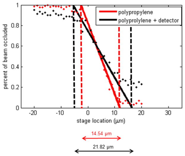
The transmission of the alpha particles through the thin detector might increase the beam size due to scattering effects. In order to quantify the amount of beam broadening, we performed two knife edge scans using a 3 μm thick layer of polypropylene; the first scan without the detector in the way, and the second scan passing through the 8.5 μm detector. These scans are shown below in figure 12.
Figure 12.
polypropylene knife edge scans of the beam before (red) and after (black) passing through the 8.5 μm detector. This graph shows the relative energy of the particles that pass through the knife edge as a function of distance. A line is fitted to the slope of the curve, and the beam size is determined by the intersection of the linear fit at fully occluded (relative energy = 0) and fully unoccluded (relative energy = 1).
The beam size increased by 50% due to scattering effects. This limits the resolution of the microbeam to 1 μm instead of 0.7 μm, and only affects experiments that require ultra high resolution [5]. For the bulk of experiments at RARAF, such as the investigation of inter-cellular communication effects, a 1 μm beam is sufficient to ensure one cell is targeted and not a bystander cell [19].
3.3 Protons (H+) measurements with the 13.5 μm transmission detector
We also placed our detectors in the path of a proton microbeam. Protons have lower LET, and deposit less energy in thin samples, and therefore are harder to detect. Only the 13.5 μm thick sample was able to detect pulses sufficiently above noise.
Figure 13(a) shows a simultaneous oscilloscope trace gathered from our 13.5 μm detector and the commercial detector above it. While it seems that a smaller amount of energy is deposited in the detector compared to alpha particles, protons are still detectable by the transmission detector. Figure 13(b) shows the distribution of pulses from the transmission detector and the commercial detector with and without passing through the transmission detector.
Figure 13.
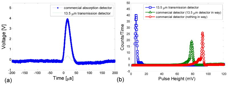
Oscilloscope trace and ADC-MCA distribution of pulse heights for protons. Enough energy appears to be deposited in the 13.5 μm detector for the detection of protons.
4. Conclusion
The main contributions of this work are the design and fabrication of a transmission particle detector that works as well as a commercial absorption detector for high-LET alpha particles in biological microbeams. We characterized 4 samples’ performance as Schottky diodes and used energy loss measurements to calculate their thicknesses. We showed that with the 8.5 μm transmission detector, 5.4 4He++ particles pass through the sample with plenty of energy to reach the commercial detector mounted above the sample. Also, we show that with the 13.5 μm transmission detector, H+ particles deposit enough energy to be detected. The implications of this are a range of new experiments able to take place at RARAF on radiation-stopping samples such as thick tissues, targets that need immersion microscopy, and integrated microfluidic devices for handling larger quantities of cells and small organisms.
Acknowledgments
This research is supported by grant number P41 EB002033 to the Radiological research Accelerator Facility from the National Institute of Biomedical Imaging and Bioengineering/National Institute of Health.
References
- 1.Voss KO, Fournier C, Taucher-Scholz G. Heavy ion microprobes: a unique tool for bystander research and other radiobiological applications. New Journal of Physics. 2008;10(7):075011. [Google Scholar]
- 2.Greubel C, Hable V, Drexler G, Hauptner A, Dietzel S, Strickfaden H, Baur I, Krücken R, Cremer T, Dollinger G, Friedl A. Competition effect in DNA damage response. Radiation and Environmental Biophysics. 2008;47(4):423–429. doi: 10.1007/s00411-008-0182-z. [DOI] [PubMed] [Google Scholar]
- 3.Zhou H, Randers-Pehrson G, Waldren CA, Vannais D, Hall EJ, Hei TK. Induction of a bystander mutagenic effect of alpha particles in mammalian cells. Proceedings of the National Academy of Sciences. 2000;97(5):2099–2104. doi: 10.1073/pnas.030420797. [DOI] [PMC free article] [PubMed] [Google Scholar]
- 4.Randers-Pehrson G, Geard CR, Johnson G, Elliston CD, Brenner DJ. The Columbia University Single-Ion Microbeam. Radiation Research. 2001;156(2):210–214. doi: 10.1667/0033-7587(2001)156[0210:tcusim]2.0.co;2. [DOI] [PubMed] [Google Scholar]
- 5.Randers-Pehrson G, Johnson GW, Marino SA, Xu Y, Dymnikov AD, Brenner DJ. The Columbia University sub-micron charged particle beam. Nuclear Instruments and Methods in Physics Research Section A: Accelerators, Spectrometers, Detectors and Associated Equipment. 2009;609(2–3):294–299. doi: 10.1016/j.nima.2009.08.041. [DOI] [PMC free article] [PubMed] [Google Scholar]
- 6.Bigelow AW, Brenner DJ, Garty G, Randers-Pehrson G. Single-Particle/Single-Cell Ion Microbeams as Probes of Biological Mechanisms. Plasma Science, IEEE Transactions on. 2008;36(4):1424–1431. [Google Scholar]
- 7.Knoll G. Radiation Detection and Measurement. 3. New York: John Wiley & Sons; 2000. [Google Scholar]
- 8.SRIM: The Stopping and Range of Ions in Matter. www.SRIM.org.
- 9.Morgan WF. Non-targeted and Delayed Effects of Exposure to Ionizing Radiation: I. Radiation-Induced Genomic Instability and Bystander Effects In Vitro. Radiation Research. 2003;159(5):567–580. doi: 10.1667/0033-7587(2003)159[0567:nadeoe]2.0.co;2. [DOI] [PubMed] [Google Scholar]
- 10.Nilsson C, Pallon J, Thungström G, Arteaga N, Auzelyte V, Elfman M, Kristiansson P, Nilsson C, Wegdén M. Evaluation of a pre-cell hit detector for the future single ion hit facility in Lund. Nuclear Instruments and Methods in Physics Research Section B: Beam Interactions with Materials and Atoms. 2006;249(1–2):924–927. [Google Scholar]
- 11.Sharma BL. Metal-Semiconductor Schottky Barrier Junctions and Their Applications. New York: Plenum Press; 1984. [Google Scholar]
- 12.Grupen C. Particle Detectors. Cambridge, UK: Cambridge University Press; 1996. [Google Scholar]
- 13.Barberet P, Balana A, Incerti S, Michelet-Habchi C, Moretto P, Pouthier T. Development of a focused charged particle microbeam for the irradiation of individual cells. Review of Scientific Instruments. 2005;76(1):015101–6. [Google Scholar]
- 14.Folkard M, Vojnovic B, Gilchrist S, Prise KM, Michael BD. The design and application of ion microbeams for irradiating living cells and tissues. Nuclear Instruments and Methods in Physics Research Section B: Beam Interactions with Materials and Atoms. 2003;210(0):302–307. [Google Scholar]
- 15.Greif KD, Brede HJ, Frankenberg D, Giesen U. The PTB single ion microbeam for irradiation of living cells. Nuclear Instruments and Methods in Physics Research Section B: Beam Interactions with Materials and Atoms. 2004;217(3):505–512. [Google Scholar]
- 16.Nilsson C, Pallon J, Thungström G, Marrero NA, Elfman M, Kristiansson P, Nilsson C, Wegdén M. Characterisation of a pre-cell hit detector to be used in single cell irradiation experiments at the Lund Nuclear Microprobe. Nuclear Instruments and Methods in Physics Research Section B: Beam Interactions with Materials and Atoms. 2008;266(21):4808–4815. [Google Scholar]
- 17.Thungström G, Westerberg L, Spohr R, Sture Petersson C. Fabrication and characterization of thin ΔE detectors for spectroscopic application. Nuclear Instruments and Methods in Physics Research Section A: Accelerators, Spectrometers, Detectors and Associated Equipment. 2005;546(1–2):312–318. [Google Scholar]
- 18.Reif F. Fundamentals of Statistical and Thermal Physics. USA: McGraw-Hill Publishing Company; 1965. [Google Scholar]
- 19.Hei TK, Zhou H, Ivanov VN, Hong M, Lieberman HB, Brenner DJ, Amundson SA, Geard CR. Mechanism of radiation-induced bystander effects: A unifying model. Journal of Pharmacy and Pharmacology. 2008;60(8):943–950. doi: 10.1211/jpp.60.8.0001. [DOI] [PMC free article] [PubMed] [Google Scholar]


