Abstract
Implantable microelectrodes provide a measure to electrically stimulate neurons in the brain and spinal cord and record their electrophysiological activity. A material with a high charge capacity such as activated or sputter-deposited iridium oxide film (AIROF or SIROF) is used as an interface. The Utah electrode array (UEA) uses SIROF for its interface material with neural tissue and oxygen plasma etching (OPE) with an aluminium foil mask to expose the active area, where the interface between the electrode and neural tissue is formed. However, deinsulation of Parylene-C using OPE has limitations, including the lack of uniformity in the exposed area and reproducibility. While the deinsulation of Parylene-C using an excimer laser is proven to be an alternative for overcoming the limitations, the iridium oxide (IrOx) suffers from fracture when high laser fluence (>1000 mJ/cm2) is used. Iridium (Ir), which has a much higher fracture resistance than IrOx, can be deposited before excimer laser deinsulation and then the exposed Ir film area can be activated by electrochemical treatment to acquire the AIROF. Characterisation of the laser-ablated Ir film and AIROF by surface analysis (X-ray photoelectron spectroscopy, scanning electron microscope, and atomic force microscope) and electrochemical analysis (electrochemical impedance spectroscopy, and cyclic voltammetry) shows that the damage on the Ir film induced by laser irradiation is significantly less than that on SIROF, and the AIROF has a high charge storage capacity. The results show the potential of the laser deinsulation technique for use in high performance AIROF-coated UEA fabrication.
Keywords: UEA, Iridium oxide, Parylene, Laser deinsulation, Photoablation, Excimer laser
1. Introduction
The electrical stimulation of cortical and other central nervous systems and recording of electrical signals from these systems require the use of penetrating microelectrodes to approach the target neurons as closely as possible (Hochberg et al., 2006; Normann, 2007). As the geometric size of an electrode is reduced to achieve better selectivity, the current density required to deliver the necessary amount of stimulation charge increases. The electrode surface material that interfaces between the electrode and neural tissue should be able to transfer the electrical current between them efficiently. Transduction of the current can take place via either double-layer capacitive coupling or a Faradaic reaction (Agnew and McCreery, 1990). Noble metals, including platinum, iridium, gold, and palladium, which present a capacitive or pseudo-capacitive coupling transduction mechanism, have been selected as the material for neural stimulating electrodes because of their resistance to corrosion. These materials are also desirable for long-term stimulation and recording applications because no chemical species are created or consumed during current stimulation. However, as the area of the electrode decreases, double-layer capacitive coupling alone is often insufficient to deliver the required charge. Materials with a Faradaic reaction transduction mechanism, where current transduction takes place through reduction and oxidation, can provide a much higher level of charge injection for the stimulation of neurons. Iridium oxide is the material with a Faradaic reaction transduction mechanism that displays the highest charge injection capacity, where the reduction and oxidation of iridium oxide film are primarily due to the valence change between Ir3+ and Ir4+ states (Cogan, 2008; Negi et al., 2010a).
There are two types of iridium oxide that are used for the fabrication of microelectrodes: activated and sputter-deposited iridium oxide film (AIROF and SIROF). AIROF is formed through electrochemical activation of the iridium film, and this reaction is accompanied by counter-ion (H+ or OH−) charge compensation from an electrolyte, as shown in Fig. 1. AIROF was the first iridium oxide film to receive attention as an oxide/chlorine catalyst in acid (Mozota and Conway, 1981) as well as for its resistance to corrosion (Johnson and Hench, 1977) and for use as an electrochromic material for display devices (Gottesfeld and McIntyre, 1979). Initially, iridium, along with other noble metals in the platinum metal group, had been studied as a neural interface material. However, activated iridium oxide was recognised as an alternative to these metals due to its higher charge storage capacity and corrosion resistance (Robblee et al, 1983). AIROF electrodes composed of iridium wire and sputtered iridium films on a silicon substrate are widely used for intracortical stimulation and recording applications. Silicon-based AIROF microelectrodes have been used as Michigan probes (Anderson et al., 1989) and in Utah electrode arrays (UEAs) (Negi et al., 2010b).
Fig. 1.
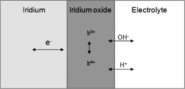
Faradaic reaction of activated iridium oxide film.
Another widely used type of iridium oxide film is SIROF, which is acquired via reactive sputtering of an iridium target in an oxidising plasma environment. SIROF exhibits cyclic voltammetric and charge storage capabilities comparable to AIROF, although its film characteristics are affected by the applied sputtering process parameters, including the deposition pressure, substrate bias, and sputtering gas composition (Negi et al, 2009).
There are various methods for removing insulation materials from microelectrodes (Fortin and Lu, 2002; Loeb et al, 1977; Schanze et al., 2007). It was recently reported that diffusion-limited deposition of Parylene on a neural probe allows electrode sites to be uncovered (von Metzen et al., 2011). However, this method is not appropriate for the deinsulation of UEAs to achieve controllable exposure and highly uniform impedance values on electrode tips. In UEAs, oxygen plasma etching (OPE) with an aluminium foil mask has conventionally been used to etch an insulation material, Parylene-C, from the electrode tip. The demand for the development of microelectrodes that exhibit sophisticated geometries with different electrode heights (Bhandari et al., 2008) in UEAs is leading a shift of deinsulation methods from oxygen plasma etching using an aluminium foil mask to laser etching, as laser etching makes the deinsulation of individual tips in the UEA possible (Yoo et al., 2012a). Furthermore, the laser deinsulation process is attractive for the large-scale production of microelectrode arrays because it is less time consuming and highly reproducible. Although laser ablation of a polymer material presents the drawback of the redeposition of carboneous debris on and around the ablated site, the surface debris can be reduced by various methods, including the use of a shielding gas (Brannon et al, 1985; Kuper and Brannon, 1992), ultrasonic cleaning (Musaev et al, 2011) and dipping in a chemical solution. Oxygen plasma treatment after laser ablation is the other alternative to remove carbon debris (Yoo et al., 2012b). It is important to minimise the amount of residual carbon debris, as this debris potentially results in biocompatibility problems in long-term stimulation and recording applications through foreign body reactions.
The selection of the electrode surface material is particularly important because the laser deinsulation of Parylene-C can produce damage to the electrode surface material, including cracking, delamination, melting, and vapourisation. While a laser fluence lower than the threshold fluence value for damaging the electrode surface material can be used, ablation of Parylene-C at a low fluence can result in incomplete removal of this substance from the laser-ablated spot (Musaev et al, 2011), causing nonuniform exposure of deinsulated tips and high deviation in impedance values.
A higher laser fluence can improve the uniformity of the exposure of the deinsulated tip and can reduce the redeposition of residual carbon debris (Liu et al., 2012). When the laser fluence is high, the momentum of the ablated by-products is sufficiently high to allow them to escape from the ablation zone into the atmosphere, resulting in less redeposition. Thus, an electrode surface material that exhibits a high resistance to the damage induced by a high laser fluence is necessary to achieve uniform and repeatable electrode tip exposure. Iridium is one potential candidate for use as an electrode surface material. Iridium displays superior physical properties, such as a very high mass density (22,560 kg m3), melting point (2466°C), and Young’s modulus (5.28 × 10⁻⁸ kPa), compared with other metals in the platinum group, which makes it resistant to high laser power-induced damages. Furthermore, it can be easily deposited on silicon-based microelectrodes via sputtering and is therefore suitable for mass microfabrication. Finally, after being exposed through laser ablation, iridium can be converted to AIROF, which exhibits a high charge injection capacity.
In this study, we investigate the resistance of sputtered iridium and iridium oxide films against damage induced by laser power. Planar iridium and AIROF electrodes deinsulated via laser ablation were fabricated and characterised using surface analysis methods (X-ray photoelectron spectroscopy, scanning electron microscopy, and atomic force microscopy) and electrochemical techniques (electrochemical impedance spectroscopy and cyclic voltammetry). Based on the determined optimised electrochemical activation parameters, 3D UEA tips with AIROF were produced using laser deinsulation and characterised.
2. Materials and methods
To investigate the effect of the laser fluence on the damage to iridium film and SIROF, iridium film and SIROF were deposited on p-type (100) c-Si wafers using DC and reactive pulsed-DC sputter deposition systems (T-M Vacuum Super series), respectively. Iridium films with three different thicknesses (50, 200 and 600 nm) were deposited on a titanium adhesion layer (50 nm) at a deposition rate of 5 nm/min in an Ar gas ambient (at a flow rate of 150 sccm and a chamber pressure of 20 mTorr). The sputtering power was 90 W. SIROF was deposited with a deposition rate of 10 nm/min in an Ar and O2 plasma ambient (flow rate of 100 sccm and chamber pressure of 10 mTorr). The sputtering power was 100 W.
Planar AIROF electrodes were also fabricated on p-type (1 0 0) c-Si wafers to investigate their electrochemical performance. Fig. 2 shows a planar view of and the fabrication process flow for the planar AIROF electrode (Negi et al., 2009). The Si wafer was deposited with a silicon nitride film acting as a dielectric insulation layer using a low-pressure chemical vapour deposition system. The film was grown for 2 h using ammonia and dichlorosilane gases with flow rates of 10 and 60 sccm, respectively. The pressure and temperature were 600 mTorr and 825°C, respectively. Titanium (50 nm) and iridium (600 nm) films were deposited sequentially with a DC sputter deposition system. LOR 7B (MicroChem, Newton, MA) and positive photoresist (Shipley Microposit S-1813, Marlborough, MA) were used to pattern the metal films via a lift-off technique. Parylene-C (3 μm) was deposited through chemical vapour deposition using the Paratech 3000 laptop deposition system (Jui-Mei et al, 2009). To improve the chemical adhesion between Parylene and the substrate, an adhesion promoter, 0.5% Silquest A-174 silane (GE, Silicones), was used. The standard photolithography technique was employed to expose the Parylene-C to the bonding pads, and the Parylene-C was then removed using a capacitively coupled plasma reactive ion etching (RIE) system (Oxford Plasmalab 80 plus). During RIE, an oxygen flow rate of 50 sccm, chamber pressure of 100 mTorr, and RF power and frequency of 75 W and 13.56 MHz, respectively, were employed. The etching time was 12 min. The Parylene film was removed from the active area of the electrode (diameter of 300 m) using an excimer laser system with a wavelength of 248 nm (Optec MicroMaster). The exposed iridium in the active area was converted to AIROF in phosphate buffered saline (PBS) at a pH of 7.4. The composition of the PBS solution was a follows: 0.13 M NaCl, 0.022 M KH2PO4·H2O, and 0.081 M Na2HPO4·7H2O. Activation was achieved by applying rectangular pulses with a cathodic bias of −0.8 to −0.95 V and an anodic bias of 0.95 V with respect to the Ag|AgCl reference electrode in PBS solution to the exposed iridium film. The frequency of the pulses was 1 Hz, and 2000 cycles of pulses were applied (Negi et al., 2010b).
Fig. 2.
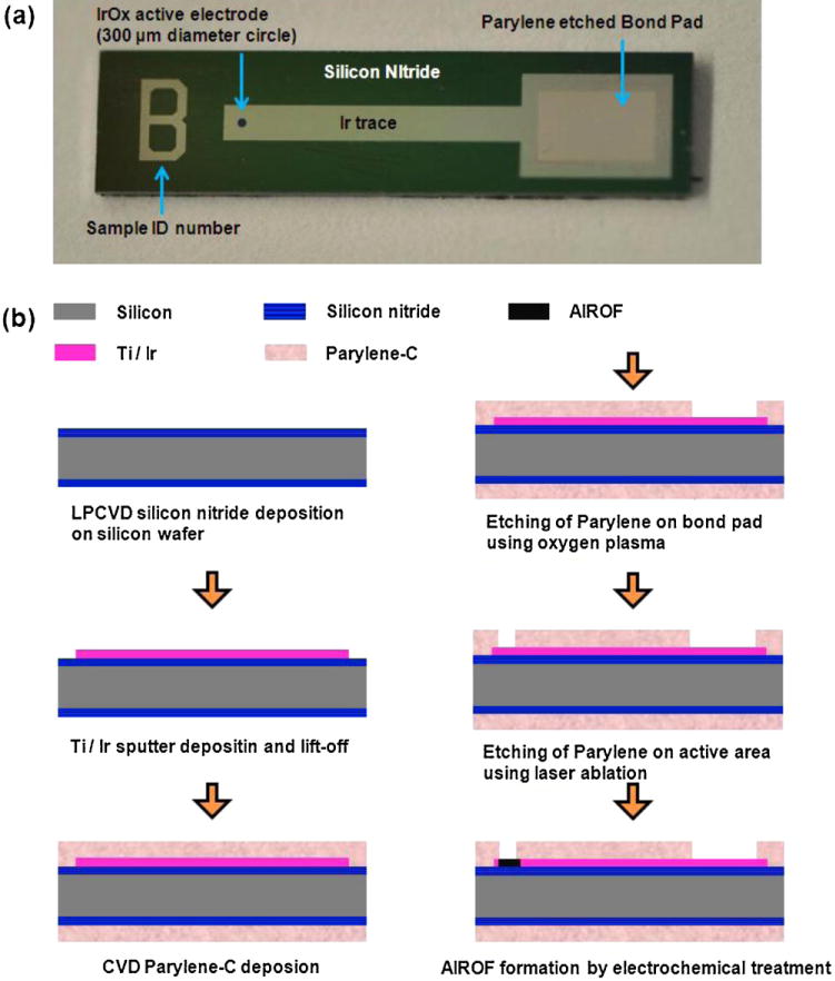
(a) Planar view of the AIROF electrode and (b) schematic process flow for planar AIROF electrode fabrication.
An AIROF Utah electrode array was fabricated through anodically oxidising Ir to AIROF following the removal of Parylene. The fabrication process for a Utah electrode array has been described in detail in other studies (Bhandari et al., 2010; Campbell et al, 1991). The same metallisation (Ti/Ir) used for the planar AIROF electrode was deposited on the electrode tips and then insulated with Parylene-C. The Parylene-C insulator material on the electrode tips was removed via focusing a demagnified excimer laser spot with a diameter of 70 μm on the Utah electrode tips. The laser pulses were 5 ns in duration, with a repetition rate of 100 Hz, and the laser fluence was 1500 mJ/cm2. The details of the laser ablation system are reported in Yoo et al. (2012a).
The morphology and roughness of the electrode surface before and after laser deinsulation were examined via scanning electron microscopy (SEM, FEI Quanta) and atomic force microscopy (AFM, Digital Instruments). Chemical and elemental analyses of the laser-ablated electrode surface were performed using XPS (Kratos Axis Ultra DLD) to examine the presence of residual carbon debris from laser-ablated Parylene. A monochromatic AlK α (180 W) X-ray source was employed, and the analysis was performed in a circular region with a diameter of 55 μm.
Sputter cleaning using 2 keV Ar+ was performed prior to XPS analysis to remove physisorbed oxygen on the film surface. Electrochemical impedance spectroscopy (EIS) and cyclic voltammetry (CV) were performed using the planar AIROF electrode in PBS solution to determine the impedance and charge storage capacity (CSC). The data were acquired using a computer-controlled commercial electrochemical test system (Gamry Instruments PC4 potentiostat). The Ag|AgCl electrode was used as a reference electrode, and a large-area Pt wire was used as a counter electrode. All potentials were measured with respect to the Ag|AgCl reference electrode. For the EIS measurements, sinusoidal signals with an amplitude of 10 mV and frequencies ranging from 1 Hz to 1 MHz were employed. Cyclic voltammograms were acquired for the potential limits of −0.6 V and 0.8 V with a sweep rate of 50 mVs−1. Following common practice, the cathodal CSC (CSCc) was used to characterise the electrodes. The CSC was calculated from the time integral for the cathodic current in a cyclic voltammogram over a potential range that is just within that of water electrolysis. For iridium oxide, the water electrolysis window was typically considered to be −0.6 V to 0.8 V with respect to the Ag|AgCl reference electrode.
3. Results and discussion
First, the effect of the laser fluence on the morphology of iridium film and SIROF was investigated. Fig. 3(a) shows backscattered SEM images of the iridium films with three different thicknesses (50 nm, 200 nm and 600 nm) exposed to 100 laser pulses with a fluence of 1920 mJ/cm2. While the iridium films with thickness of 50 and 200 nm showed cracks, there were no fractures observed on the iridium film with a thickness of 600 nm at a laser fluence of 1920 mJ/cm2. Fig. 3(b) shows backscattered SEM images of SIROF with a film thickness of 600 nm illuminated using 100 laser pulses with different laser fluences (960, 720, and 480 mJ/cm2). As can be seen in the figure, the SIROF was damaged under laser fluences higher than 720 mJ/cm2. The results presented in Fig. 3 indicate that iridium film shows much a higher resistance against damage due to high laser power compared with SIROF.
Fig. 3.
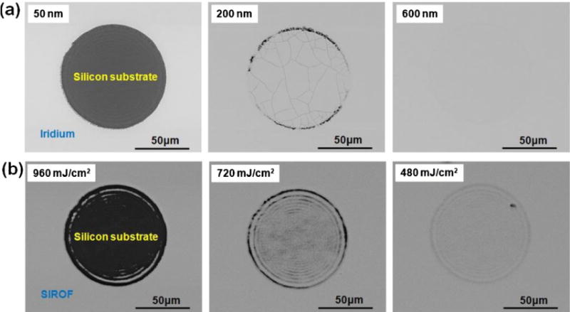
(a) Backscattered SEM images of iridium films with three different thicknesses (50 nm, 200 nm, and 600 nm) exposed to 100 laser pulses with a fluence of 1920 mJ/cm2. (b) Backscattered SEM images of SIROF(600 nm) exposed to different laser fluences (960, 720, and 480 mJ/cm2).
Fig. 4(a) displays an optical image of a laser-ablated spot (diameter of 100 μm) formed on a polished soda-lime glass substrate coated with Parylene (thickness of 3 μm). While Parylene was clearly removed within the circle, debris remained around the edge of the circle. Fig. 4(b) provides the hump heights at the edge of circles ablated using different fluences (~290, 630, 860, and 1300 mJ/cm2) immediately after laser ablation (left) and after 2 min of OPE treatment (right). The profiles were measured with a Tencor profilometer (Profilometer Tencor P-20H). The lower the applied laser fluence, the higher the humps were found to be. During laser ablation, the laser breaks down Parylene into molecular fragments, and carbon debris is ejected from the ablation zone into the air. When the momentum of the carbon debris is not sufficient, it can be redeposited in the vicinity of the ablation area due to momentum exchange with the atmosphere. When the laser fluence is high, the momentum of the carbon debris can be sufficiently high to escape the ablation zone into the atmosphere, resulting in lower hump heights. The hump heights were decreased by OPE treatment. The carbon residue redeposited around the exposed area can potentially produce biocompatibility problems in long-term stimulation and recording applications due to foreign body reactions.
Fig. 4.
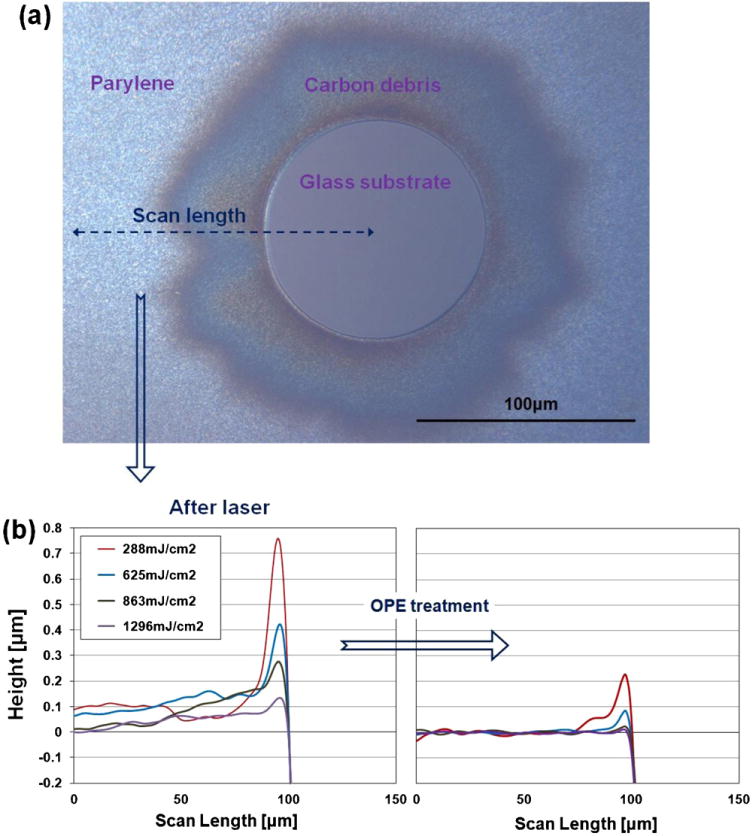
(a) Optical image of a laser-ablated spot (diameter of 100 μm) on a soda-lime glass. (b) Surface profiles of the edges of circles ablated using different laser fluences (left) and after 2 min of OPE treatment (right).
Fig. 5 provides the X-ray photoemission spectra of a planar iridium electrode sample coated with Parylene-C before and after laser ablation. As shown in Fig. 5(a) and (b), in the as-deposited Parylene-C, there are peaks corresponding to the rings and chain carbons of Parylene (C—(C, H)), oxygen contamination peaks (C—O) originating from water absorption on the surface, and spin orbit split Cl 2p peaks. Fig. 5(c) and (d) provides the X-ray photoemission spectra of the region of carbon debris shown in Fig. 4(a), revealing that the Parylene was decomposed, leaving carbon debris purely consisting of carbon elements (C—C) behind.
Fig. 5.
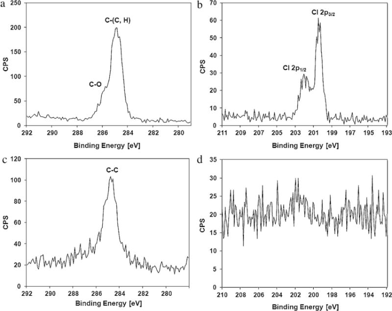
X-ray photoemission spectra of (a) the C 1s peak of as-deposited Parylene-C, (b) the Cl 2p peak of as-deposited Parylene-C, (c) the C 1s peak of laser-ablated Parylene-C and (d) the Cl 2p peak of laser-ablated Parylene-C.
Based on the above experimental results, planar AIROF electrodes were fabricated and characterised. Laser deinsulation of a 300 μm-diameter circle on iridium film (thickness of 600 nm) coated with Parelene (thickness of 3 μm) was performed using laser pulses of 50 with a fluence of 1500 mJ/cm2. Fig. 6(a) shows SEM images of the laser-deinsulated circle immediately after laser illumination (left) and after 2 min of subsequent OPE treatment (right). Activation of iridium film to produce AIROF was achieved by applying rectangular pulses (with levels of −0.8 and 0.95 V with respect to the Ag|AgCl reference electrode) in PBS solution. Two thousand cycles of pulses with a repetition rate of 1 Hz were applied. Fig. 6(b) shows SEM images of iridium film (left) and AIROF (right). After activation, the roughness of the film was increased. Fig. 6(c) shows AFM images of iridium film (left) with an rms roughness of 2.7 nm and AIROF (right) with an rms roughness of 11.3 nm.
Fig. 6.
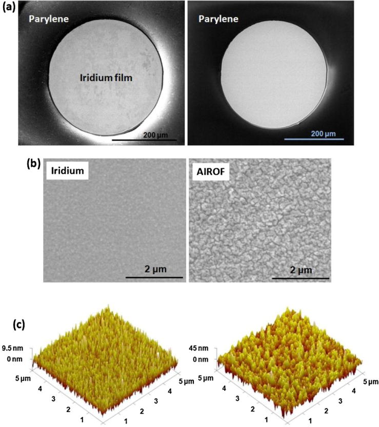
(a) SEM images of laser deinsulated holes in a Parylene-coated iridium film before (left) and after (right) OPE treatment. (b) SEM images of iridium film (left) and AIROF film (right). (c) AFM images of iridium film (left) and AIROF film (right).
Fig. 7(a) and (b) provides the X-ray photoemission spectra obtained before the electrochemical activation of the iridium film, and Fig. 7(c) and (d) provides those of AIROF. Fig. 7(a) shows sharp peaks for spin orbit split Ir 4f. However, as shown in Fig. 7(b), there was no O 1s peak. On the other hand, Fig. 7(c) shows broadened Ir 4f peaks, and Fig. 7(d) shows an apparent O1s peak. Because the AIROF sample contained iridium atoms of different valences in tetravalent or trivalent form, the full-width half-maximum (1.25 eV) of Ir4f7/2 in AIROF was wider than that (0.9 eV) of pure iridium. The broadened asymmetric O1s peak shown in Fig. 7(d) can be attributed to hydroxides, adsorbed water, or water from hydration (Kodintsev et al., 1992).
Fig. 7.
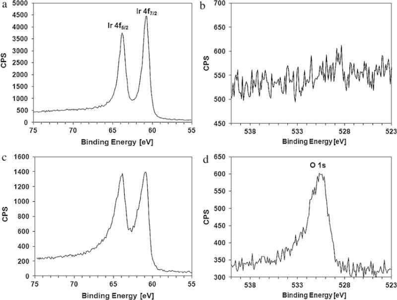
X-ray photoemission spectra showing (a) the Ir 4f peak for the as-deposited iridium film, (b) the O 1s peak for the as-deposited iridium film, (c) the Ir 4f peak of the AIROF and (d) the O1s peak of the AIROF.
Fig. 8(a) shows SEM images of AIROF activated using rectangular pulse levels of −0.85 and 0.95 V (left), −0.9 and 0.95 V (centre), and −0.95 and 0.95 V (right). Among the many parameters of the activation pulse signal for the growth of AIROF, including the anodic/cathodic voltage, ramp-up rate, dwell time, and number of pulses, the cathodic voltage was analysed in detail because it is one of the most critical parameters for tuning the film growth rate (Pickup and Birss, 1987). A crack in started to appear the AIROF at a cathodic voltage of −0.85 V, and the degradation of the film morphology became more severe as the cathodic voltage became more negative, as shown in Fig. 8(b). The AIROF partially flaked off at −0.9 V and completely flaked off at −0.95 V. Behaviour similar to that of the AIROF fabricated on wire-type iridium electrodes has previously been reported (Cogan et al, 2004). Although the AIROF activated using pulse levels of −0.8 and 0.95 V showed a stable morphology without cracks, a long-term analysis of the stimulation of AIROF electrodes under an in vivo environment is required for chronic implantation applications.
Fig. 8.
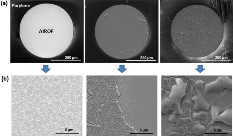
(a) SEM images of AIROF produced using rectangular pulse levels of −0.85 and 0.95 V (left), −0.9 and 0.95 V (centre), and −0.95 and 0.95 V (right). (b) Magnified images of (a).
The Bode plot of the impedance values for planar electrodes with an iridium active area and AIROF active area are presented in Fig. 9. The active area was circular in shape and has a diameter of 300 μm (geometric area of approximately 70,600 μm2). The thickness of the iridium film was 600 nm. The active area was exposed via deinsulation of Parylene using laser pulses of 50 with a fluence of 1500 mJ/cm2. The impedance of the planar iridium electrode fabricated through laser ablation only was 28 kΩ at 1 kHz. However, it was decreased significantly, down to ~5 kΩ, by 2 min of subsequent OPE treatment. This value was similar to that of an electrode fabricated only via OPE deinsulation (for 12 min). After the activation of iridium, the impedance decreased to ~0.9 kΩ. The impedance of the planar iridium electrode showed a capacitor-like frequency dependence, indicating that the current transduction mechanism in this case is capacitive coupling. On the other hand, the impedance of the planar AIROF electrode showed resistive behaviour for the frequency range from 50 Hz to 50 kHz. The impedances converged at a frequency range over 50 kHz, which indicates the effect of PBS impedance. The results indicate that the planar AIROF electrode fabricated using the hybrid deinsulation method (laser deinsulation followed by 2 min of OPE) (Yoo et al., 2012b) shows resistive behaviour and provides much lower impedance.
Fig. 9.
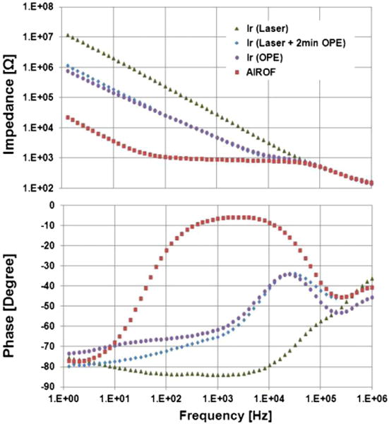
Amplitude (upper) and phase (bottom) of the impedance of planar electrodes with an iridium active area formed using three different deinsulation conditions and with an AIROF active area (area of the active region ≈ 70,600 μm2).
Cyclic voltammograms for the planar iridium electrode fabricated via laser ablation followed by 2 min of OPE and the planar AIROF electrode, measured in PBS solution, are illustrated in Fig. 10. The voltammogram for the planar iridium electrode exhibited an approximately rectangular shape, which is expected for an electrode presenting a double-layer capacitive coupling transduction mechanism. However, the voltammogram for the planar AIROF electrode showed main current peaks at 0.25 V and −0.21 V, corresponding to reversible Ir3+ and Ir4+ redox reactions, respectively. The CSCc was 3.5 mC/cm2 for the planar iridium electrode and 10 mC/cm2 for the planar AIROF electrode. The much higher charge storage capacity of the planar AIROF electrode is attributed to its Faradaic transduction mechanism.
Fig. 10.
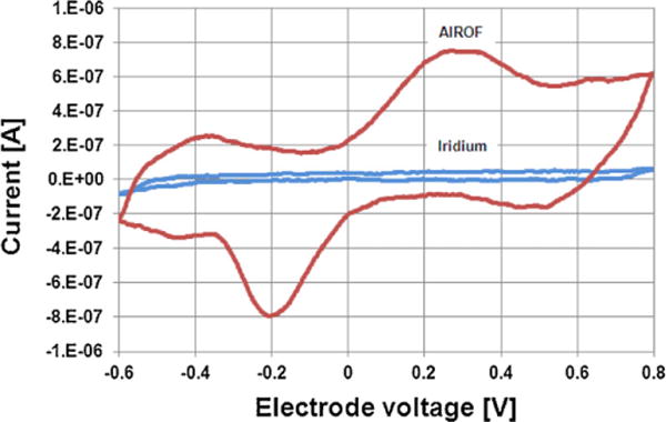
Cyclic voltammograms for the planar iridium and AIROF electrodes (area of the active region ≈ 70,600 μm2). The electrode voltage was measured with respect to the Ag|AgClreference electrode.
Fig. 11(a) shows the Utah electrode array tips fabricated through laser deinsulation using 100 pulses with a fluence of 1500 mJ/cm2 on iridium (left) and 500 pulses of with a fluence of 700 mJ/cm2 on SIROF (right). The laser-ablated electrode array tip produced using a high fluence (100 pulses and a fluence of 1500 mJ/cm2) showed a distinctive boundary line between the exposure area and Parylene, and the deinsulated iridium surface looked clean. On the other hand, the laser-ablated electrode array tip generated using a low fluence (500 pulses with a fluence of 700 mJ/cm2) exhibited an indistinct boundary and insufficiently etched Parylene on the sidewall of the tip. A low laser fluence of 700 mJ/cm2 was used to prevent fractures in the SIROF, which resulted in nonuniform removal of Parylene and, thus, a high impedance value as well as large variation between electrode tips. Fig. 11(b) shows SEM images of the as-deposited iridium film (left), AIROF activated using rectangular pulses with levels of −0.8 and 0.95 V (centre), and AIROF activated using rectangular pulses with levels of −0.85 and −0.95 V (right). The morphological change in the AIROF fabricated via the activation of iridium film on Utah electrode array tips for different bias conditions was similar to that for the planar electrodes.
Fig. 11.
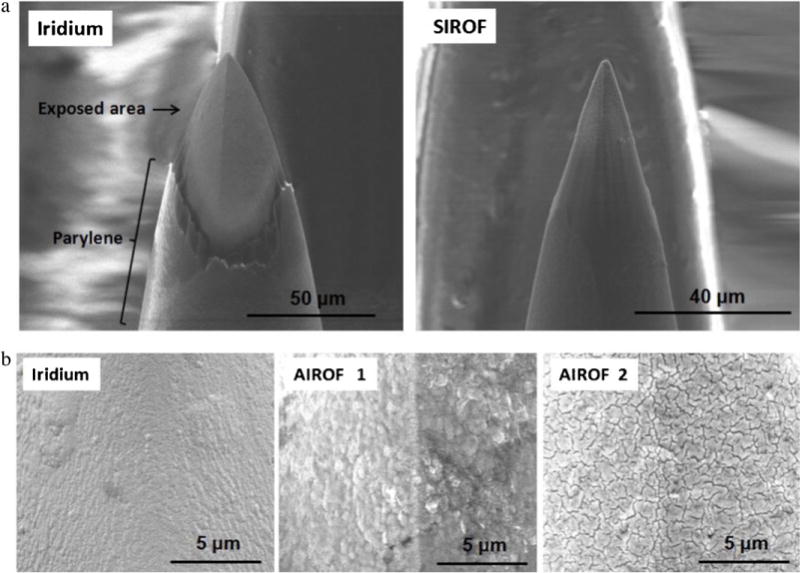
(a) SEM images of laser-deinsulated Utah electrode array tips with iridium film (left) and SIROF (right). (b) SEM images of an as-deposited iridium film (left), AIROF activated using rectangular pulses with levels of −0.8 and 0.95 V (centre), and AIROF activated using rectangular pulses with levels of −0.85 and 0.95 V (right).
Bode plots of the impedance of the AIROF Utah electrode are presented in Fig. 12(a). The geometrical surface area of the electrode tip with an exposure of 60 μm was calculated to be approximately 6000 μm2, assuming that the tip was identical to a cone (Negi et al, 2010a). The impedance of the AIROF UEA tip was ~3 kΩ for the frequency range of 103 to 105 Hz. The behaviour of the AIROF UEA tip characterised through EIS and CV was similar to that of the planar AIROF electrode. The CSCc calculated using CV was ~16 mC/cm2, which agrees well with the value reported in the literature (Cogan, 2008).
Fig. 12.
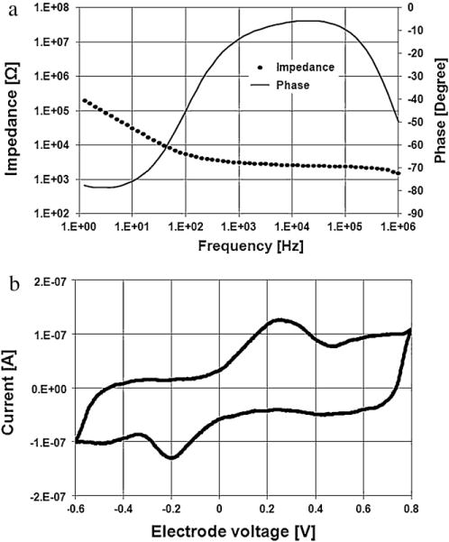
EIS (a) and CV (b) of the AIROF Utah microelectrode (geometric surface area ≈ 6000 μm2).
4. Conclusions
The characteristics of AIROF-coated UEA tips deinsulated via laser ablation were investigated. Unlike UEA tips produced using SIROF, UEA tips with Ir can be deinsulated using a high laser fluence to achieve a low electrochemical impedance value and high charge storage capacity. The results indicate that laser deinsulation of electrode tips with iridium film and subsequent activation of the iridium film represents a suitable method for the fabrication of high-performance silicon-based implantable devices.
HIGHLIGHTS.
-
►
The iridium film exhibits a much higher resistance to damage due to high laser power.
-
►
The lower the laser fluence, the higher the humps of carbon debris.
-
►
An electrode array tip laser ablated using a high fluence shows a distinctive boundary line between the exposure area and Parylene.
-
►
Laser deinsulation of electrode tips with iridium film and subsequent activation of the iridium film are suitable for fabrication of high-performance silicon-based implantable devices.
Acknowledgments
This work was supported by the WCU (R31-2008-000-10026-0) and Bio-imaging Research Program at GIST and DARPA award N66001-06-C-4056 and NIH (1R01NS064318-01A1). Sample fabrication, laser deinsulation, and film characterisation were performed in the Utah Nanofabrication Laboratory and Surface and Nanoimaging Laboratory of the University of Utah. We would like to thank Dr. Brian van Devener for assistance in collecting XPS and SEM data, and we also appreciate the help of the UEA production team with the electrode arrays. Sandeep Negi has a financial interest in the company Blackrock Microsystems, which develops and produces implantable neural interfaces and electrophysiological equipment and software.
References
- Agnew WF, McCreery DB. Neural prostheses: fundamental studies. Englewood Cliffs, NJ: Prentice Hall; 1990. [Google Scholar]
- Anderson DJ, Najafi K, Tanghe SJ, Evans DA, Levy KL, Hetke JF, et al. Batch fabricated thin-film electrodes for stimulation of the central auditory system. IEEE Trans Biomed Eng. 1989;36:693–704. doi: 10.1109/10.32101. [DOI] [PubMed] [Google Scholar]
- Bhandari R, Negi S, Rieth L, Normann RA, Solzbacher F. A novel method of fabricating convoluted shaped electrode arrays for neural and retinal prostheses. Sens Actuators A: Phys. 2008:145–146. 123–30. doi: 10.1016/j.sna.2007.10.072. [DOI] [PMC free article] [PubMed] [Google Scholar]
- Bhandari R, Negi S, Rieth L, Solzbacher F. A wafer-scale etching technique for high aspect ratio implantable MEMS structures. Sens Actuators A: Phys. 2010;162:130–6. doi: 10.1016/j.sna.2010.06.011. [DOI] [PMC free article] [PubMed] [Google Scholar]
- Brannon JH, Lankard JR, Baise AI, Burns F, Kaufman J. Excimer laser etching of polyimide. J Appl Phys. 1985;58:2036–43. [Google Scholar]
- Campbell PK, Jones KE, Huber RJ, Horch KW, Normann RA. A silicon-based, three dimensional neural interface: manufacturing processes for an intra cortical electrode array. IEEE Trans Biomed Eng. 1991;38(38):758–68. doi: 10.1109/10.83588. [DOI] [PubMed] [Google Scholar]
- Cogan SF. Neural stimulation and recording electrodes. Annu Rev Biomed Eng. 2008;10:275–309. doi: 10.1146/annurev.bioeng.10.061807.160518. [DOI] [PubMed] [Google Scholar]
- Cogan SF, Guzelian AA, Agnew WF, Yuen TGH, McCreery DB. Over-pulsing degrades activated iridium oxide films used for intracortical neural stimulation. J Neurosci Methods. 2004;137:141–50. doi: 10.1016/j.jneumeth.2004.02.019. [DOI] [PubMed] [Google Scholar]
- Fortin JB, Lu TM. A model for the chemical vapor deposition of poly(para-xylylene) (Parylene) thin films. Chem Mater. 2002;14:1945–9. [Google Scholar]
- Gottesfeld S, McIntyre JDE. Electrochromism in anodic iridium oxide films. J Electrochem Soc. 1979;126:742–50. [Google Scholar]
- Hochberg LR, Serruya MD, Friehs GM, Mukand JA, Saleh M, Caplan AH, et al. Neuronal ensemble control of prosthetic devices by a human with tetraplegia. Nature. 2006;442:164–71. doi: 10.1038/nature04970. [DOI] [PubMed] [Google Scholar]
- Johnson PF, Hench LL. An in vitro analysis of metal electrodes for use in the neural environment. Brain Behav Evol. 1977;14:23–45. doi: 10.1159/000124612. [DOI] [PubMed] [Google Scholar]
- Jui-Mei H, Rieth L, Normann RA, Tathireddy P, Solzbacher F. Encapsulation of an integrated neural interface device with Parylene C. IEEE Trans Biomed Eng. 2009;56:23–9. doi: 10.1109/TBME.2008.2002155. [DOI] [PubMed] [Google Scholar]
- Kodintsev IM, Trasatti S, Rubel M, Wieckowski A, Kaufher N. X-ray photoelectron spectroscopy and electrochemical surface characterization of iridium(IV) oxide + ruthenium(IV) oxide electrodes. Langmuir. 1992;8:283–90. [Google Scholar]
- Kuper S, Brannon J. Ambient gas effects on debris formed during KrF laser ablation of polyimide. Appl Phys Lett. 1992;60:1633–5. [Google Scholar]
- Liu K, NiCkolov Z, Oh J, Noh HM. KrF excimer laser micromachining of MEMS materials: characterization and applications. J Micromech Microeng. 2012;22:015012. [Google Scholar]
- Loeb GE, Bak MJ, Salcman M, Schmidt EM. Parylene as a chronically stable, reproducible microelectrode insulator. IEEETrans Biomed Eng. 1977;BME-24:121–8. doi: 10.1109/TBME.1977.326115. [DOI] [PubMed] [Google Scholar]
- Mozota J, Conway BE. Modification of apparent electrocatalysis for anodic chlorine evolution on electrochemically conditioned oxide films at iridium anodes. J Electrochem Soc. 1981;128:2142–9. [Google Scholar]
- Musaev O, Scott P, Wrobel J, Wolf J, Kruger M. UV laser ablation of Parylene films from gold substrates. J Mater Sci. 2011;46:183–7. [Google Scholar]
- Negi S, Bhandari R, Rieth L, Solzbacher F. Effect of sputtering pressure on pulsed-DC sputtered iridium oxide films. Sens Actuators B: Chem. 2009;137:370–8. [Google Scholar]
- Negi S, Bhandari R, Rieth L, Solzbacher F. In vitro comparison of sputtered iridium oxide and platinum-coated neural implantable microelectrode arrays. Biomed Mater. 2010a;5:015007. doi: 10.1088/1748-6041/5/1/015007. [DOI] [PubMed] [Google Scholar]
- Negi S, Bhandari R, Rieth L, Wagenen RW, Solzbacher F. Neural electrode degradation from continuous electrical stimulation: comparison of sputtered and activated iridium oxide. J Neurosci Methods. 2010b:8–17. doi: 10.1016/j.jneumeth.2009.10.016. [DOI] [PMC free article] [PubMed] [Google Scholar]
- Normann RA. Technology insight: future neuroprosthetic therapies for disorders of the nervous system. Nat Clin Pract Neurol. 2007;3:444–52. doi: 10.1038/ncpneuro0556. [DOI] [PubMed] [Google Scholar]
- Pickup PG, Birss VI. A model for anodic hydrous oxide growth at iridium. J Electroanal Chem Interf. 1987;220:83–100. [Google Scholar]
- Robblee LS, Lefko JL, Brummer SB. Activated Ir:. An electrode suitable for reversible charge injection in saline solution. J Electrochem Soc. 1983;130:731–3. [Google Scholar]
- Schanze T, Hesse L, Lau C, Greve N, Haberer W, Kammer S, et al. An optically powered single-channel stimulation implant as test system for chronic biocompatibility and biostability of miniaturized retinal vision prostheses. IEEE Trans Biomed Eng. 2007;54:983–92. doi: 10.1109/TBME.2007.895866. [DOI] [PubMed] [Google Scholar]
- von Metzen RP, Lass N, Ruther P, Stieglitz T. Diffusion-limited deposition of Parylene C. J Microelectromech Syst. 2011;20:239–50. [Google Scholar]
- Yoo J-M, Sharma A, Tathireddy P, Rieth LW, Solzbacher F, Song JI. Excimer-laser deinsulation of Parylene-C coated Utah electrode array tips. Sens Actuators B: Chem. 2012a:166–167. 777–86. [Google Scholar]
- Yoo J-M, Song J-I, Tathireddy P, Solzbacher F, Rieth LW. Hybrid laserand reactive ion etching of Parylene-C for deinsulation of a Utah electrode array. J Micromech Microeng. 2012b;22:105036. [Google Scholar]


