Abstract
The deformation of nanocomposites containing graphene flakes with different numbers of layers has been investigated with the use of Raman spectroscopy. It has been found that there is a shift of the 2D band to lower wavenumber and that the rate of band shift per unit strain tends to decrease as the number of graphene layers increases. It has been demonstrated that band broadening takes place during tensile deformation for mono- and bilayer graphene but that band narrowing occurs when the number of graphene layers is more than two. It is also found that the characteristic asymmetric shape of the 2D Raman band for the graphene with three or more layers changes to a symmetrical shape above about 0.4% strain and that it reverts to an asymmetric shape on unloading. This change in Raman band shape and width has been interpreted as being due to a reversible loss of Bernal stacking in the few-layer graphene during deformation. It has been shown that the elastic strain energy released from the unloading of the inner graphene layers in the few-layer material (∼0.2 meV/atom) is similar to the accepted value of the stacking fault energies of graphite and few layer graphene. It is further shown that this loss of Bernal stacking can be accommodated by the formation of arrays of partial dislocations and stacking faults on the basal plane. The effect of the reversible loss of Bernal stacking upon the electronic structure of few-layer graphene and the possibility of using it to modify the electronic structure of few-layer graphene are discussed.
Keywords: graphene, Bernal stacking, nanocomposites, Raman spectroscopy, deformation
Graphene is currently inspiring a whole range of research activities in a number of scientific areas such as physics and materials science because of its interesting and unusual electronic and mechanical properties.1,2 Excitement was generated originally because monolayer graphene was the world’s first 2D atomic crystal and the thinnest material every produced.3 It was found to be extremely electrically conductive, with its charge carriers being massless Dirac fermions,4 and to have unprecedented levels of stiffness and strength,5 consistent with theoretical predictions.6 Bilayer graphene in which the two layers of carbon atoms are in so-called AB Bernal stacking7 has strikingly different electronic properties and has a pair of high-energy electronic sub-bands.8 It is also unusual in that it has a band gap that can be controlled directly by the size of a current applied across the layers.1 Similar behavior is found with trilayer graphene making these few-layer, Bernal stacked graphene materials strong candidates for optoelectronic and nanoelectronic applications.9 Although the majority of graphene prepared by mechanical exfoliation has a high proportion of Bernal stacked material, the situation is not the same for multilayer material produced by CVD or epitaxial growth where a number of different stacking configurations may be encountered.9 In such cases, differences in the stacking sequences and relative twist between the different layers gives rise to materials with different optical and electronic properties.10−12 It is important therefore to have accurate and reliable methods of determining the nature and quality of the stacking of the graphene layers in multilayer material.
A number of different experimental techniques can be used to characterize the stacking sequences in few-layer graphene and the most direct method is transmission electron microscopy (TEM).9,13−16 Twisting and rotation of the graphene layers leads to the loss of Bernal stacking7 and the degree of misalignment can be evaluated from electron diffraction or Moiré patterns. It is even possible to image the misaligned structures using atomic resolution bright field and high angle annular dark field TEM where good correlation is found between the experimental and simulated images.15 Raman spectroscopy is also a very useful technique to evaluate the stacking of the graphene layers in few-layer material.16−20 There are major differences between the form of the 2D (or G′) band between samples of graphene that are either Bernal stacked or have twisted layers; it is relatively broad and asymmetric in Bernal stacked material and significantly narrower and more symmetric in twisted or turbostratic stacked graphene layers. It is also possible to distinguish between ABA Bernal-stacked or ABC rhombohedral stacked trilayer material from the form of the 2D Raman band.18,19 Synchrotron-based infrared absorption spectroscopy has been employed to show that the electronic structure of mechanically exfoliated few-layer graphene in which there is either ABA or ABC stacking depends strongly upon the stacking sequence.21 Scanning tunneling microscopy (STM)22 and spectroscopy are particularly useful techniques to understand the effect of stacking upon the electronic structure of few-layer graphene as they can simultaneously measure the local twist angle, the Fermi velocity and the degree of interlayer coupling.23 It has been found for CVD-grown material that the low energy carriers start to exhibit Landau level spectra characteristic of massless Dirac fermions for twist angles of over about 3° and that above 20° the layers effectively decouple with their electronic properties becoming similar to those of single-layer graphene.23
It is well established that Raman spectroscopy is one of the most versatile methods of both characterizing graphene and following its deformation in nanocomposites.24−26 Strong, well-defined resonance Raman spectra are obtained even from single atomic graphene layers and the technique can be used relatively easily to differentiate between monolayer, bilayer, trilayer and few-layer material, from the shape and position of the 2D (or G′) Raman band.27−29 It is also found that the positions of the Raman bands in graphene shift with stress30−39 and that such stress-induced Raman band shifts can be used to determine the stress in the material and so determine its effective Young’s modulus.38 These stress-induced band shifts have been used to monitor the transfer of stress between a polymer matrix and the graphene reinforcement in model nanocomposites consisting of monolayer24,25 or few-layer26 graphene flakes sandwiched between thin polymer films. The behavior of model monolayer nanocomposites has been shown to follow classical shear-lag behavior at low strains with evidence of failure of the graphene–polymer interface24,25 coupled with matrix cracking.25 There is a recent report of graphene cracking39 at higher strain levels and the loss of Bernal stacking in bilayer graphene near a boundary with monolayer material. In the case of model nanocomposites reinforced with few-layer graphene, the behavior has been found to be more complex with evidence of inferior levels of stress transfer even at low strains. This has been modeled in terms of poorer stress transfer between the inner graphene layers than between the polymer matrix and the outer graphene layers.26
The present study is concerned with understanding the mechanism behind this poor internal stress transfer within few-layer graphene. There is accumulated evidence in the literature going back over 40 years that basal plane slip can take place easily in graphite.40−42 Early TEM studies of thin graphite “foils” showed that extensive faulting could take place on the basal plane of graphite giving rise to arrays of dislocation ribbons and stacking faults.40,41 It was shown that it is favorable energetically for full dislocations on the basal plane to dissociate into two partial dislocations with a stacking fault between them40 and that the separation of the partials is typically 100 nm.41 This process takes place without breaking the in-plane C–C bonds and the strain is accommodated by distortion of the graphene hexagons in the vicinity of the dislocation core. A typical stacking fault would contain a region of rhombohedral ABC rather than hexagonal ABA stacking and the stacking fault energy on the basal plane of graphite has been shown to be very low,42 in the order of only 1 mJ m–2. This behavior is related to the relatively low value of c44, the elastic constant for basal plane shear, which is thought to be only of the order of 5 GPa.42 Another parameter that gives further insight into the ease of movement of the dislocations and their diffuse nature is the vanishingly small value of Peierls stress of 10–17 Pa that has been calculated for a partial basal edge dislocation in graphite.42 In a very recent study it was shown that Raman spectroscopy could also be used to monitor the interlayer shear mode of few-layer graphenes.43 The position of the low-frequency Raman band that appears at around 42 cm–1 in graphite is found to be sensitive to the number of layers in few-layer graphene and falls to 31 cm–1 in bilayer material. This E2g mode Raman band, which is not accessible using conventional spectrometer geometries, has been termed “C”.43 Its dependence upon the number of layer has been explained using a linear chain model and this has enabled the value of the elastic constant for basal plane shear to be determined as c44 = 4.3 GPa.
Results and Discussion
In this present study we have followed the effect of deformation upon the 2D band in the Raman spectra of a number of model nanocomposites consisting of exfoliated monolayer, bilayer, trilayer and few-layer graphene flakes embedded in a polymer matrix on a poly(methyl methacrylate) (PMMA) beam.26 We have monitored the changes with strain in position and fwhm (full width at half-maximum height) of the bands fitted to a single peak.
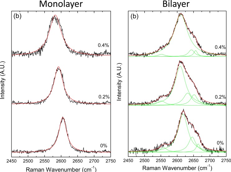
The shift of the 2D band with strain for monolayer and bilayer graphene is shown in Figure 1. It can be seen that both bands shift to lower wavenumber and broaden as the tensile strain is increased, with some evidence of the band splitting for the monolayer graphene at the higher strain levels that has been discussed at length in the literature.35,36 Details of the behavior are shown in Figures S1 and S2 of the Supporting Information. The 2D band shift per unit strain is similar for both the monolayer material,26,39 and the bilayer band, which actually consists of 4 sub-bands,27−29 appears to undergo broadening even when fitted to a single Lorentzian peak (Figure S2). The fwhm (full width at half-maximum) of the 2D band increases from 28 to 44 cm–1 for the monolayer and from 48 to 59 cm–1 for the bilayer (fitted to a single peak) up to 0.4% strain.
Figure 1.
Shifts of the 2D Raman band with strain for graphene flakes in a model nanocomposite. Overall band shift for (a) the monolayer and (b) the bilayer materials.
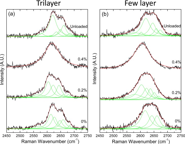
In contrast to the monolayer and bilayer materials, the stress-induced 2D band shift behavior of the trilayer and few-layer graphene in the nanocomposites is quite different as can be seen in Figure 2. The few-layer graphene was probably a tetralayer flake, but it is difficult to be sure of the exact number of layers in thin graphene flakes with more than 3 layers. In both cases the 2D band, fitted arbitrarily to 6 peaks,28 shifts to lower wavenumber with tensile strain and changes shape. It can be seen from Figure 2 that the shape of the Raman bands change markedly during deformation, becoming narrower and more symmetric at 0.4% strain. It can also be fitted to single Lorentzian peaks, similar to, but broader than, that of the monolayer material in Figure 1. Moreover, when the stress is removed, the Raman bands shift back to higher wavenumber and the shape and width of the bands revert to those of the materials before deformation. Deformation was limited to 0.4% strain to avoid complications from failure of the graphene/polymer interfaces seen in our earlier studies.24,25 Details of the behavior for the trilayer and few-layer materials are shown in Figures S3 and S4 of the Supporting Information. The 2D band shift rate per unit strain for the specimens containing material with more than two layers is found to be significantly lower than that for monolayer graphene, as has been found before,26 and the band shows considerable narrowing with tensile strain (see Supporting Information). The fwhm for the 2D band decreases from 71 to 67 cm–1 for the trilayer and from 88 to 78 cm–1 for the few-layer material (all fitted to single Lorenztian peaks) up to 0.4% strain.
Figure 2.
Shifts of the 2D Raman band with strain for graphene flakes in a model nanocomposite. Overall band shift for (a) the trilayer and (b) the few-layer materials.
It is well established that for few-layer graphene, Raman spectroscopy can be used to distinguish between materials in which the layers are either stacked randomly or in regular Bernal AB stacking.16−20 For random stacking, the appearance of the 2D band is symmetric and similar to that of the monolayer graphene but broadened, whereas in the case of Bernal stacking, the bands are broad and asymmetric.17 The clear conclusion of the behavior shown in Figure 2 is that for both the trilayer and few-layer graphene Bernal AB stacking is lost in the material by around 0.4% strain but is restored on unloading the nanocomposite specimen. Mapping of the 2D band after unloading (Figure S7, Supporting Information) has shown a larger scatter in the bandwidth than before deformation implying that the Bernal stacking is not completely regained throughout the flake.
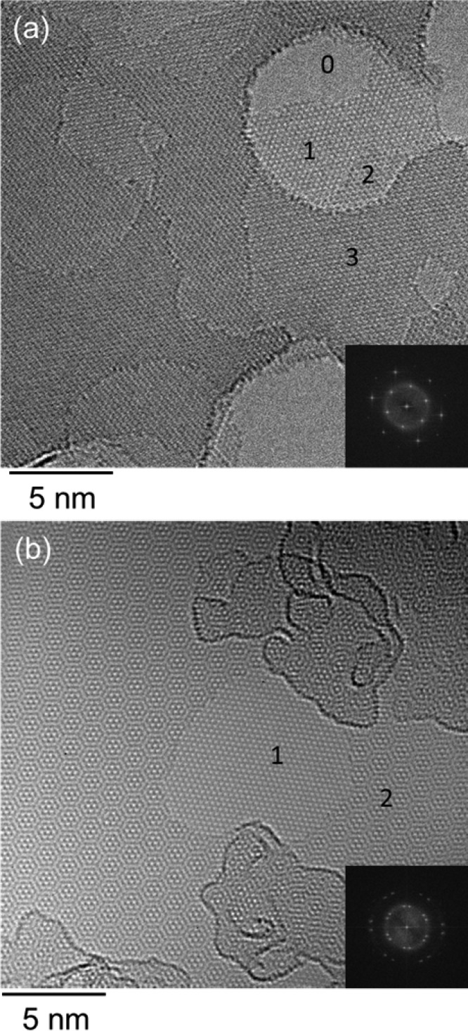
The multilayer graphene produced by the mechanical exfoliation procedure,2 used in this present study, generally shows Bernal stacking unless it is folded. It is possible to visualize the differences between Bernal and non-Bernal stacked material using transmission electron microscopy by comparing exfoliated few-layer graphene samples with graphene grown by chemical vapor deposition (CVD), where non-Bernal stacking is more commonly found, as shown in Figure 3. In the case of the Bernal stacking shown in Figure 3a, the FFT (fast Fourier transform) of the high resolution image shows a single orientation of the graphene with similar atomic arrangements being resolved in all layers. In Figure 3b, the FFT shows that one layer is rotated relative to the other and a characteristic Moiré pattern is found in the region of bilayer material.13−15
Figure 3.
High resolution electron micrographs and associated FFTs of the images for (a) chemically exfoliated graphene showing Bernal stacking and (b) CVD-grown graphene showing non-Bernal stacking (the numbers indicate the different number of layers present in the different regions).
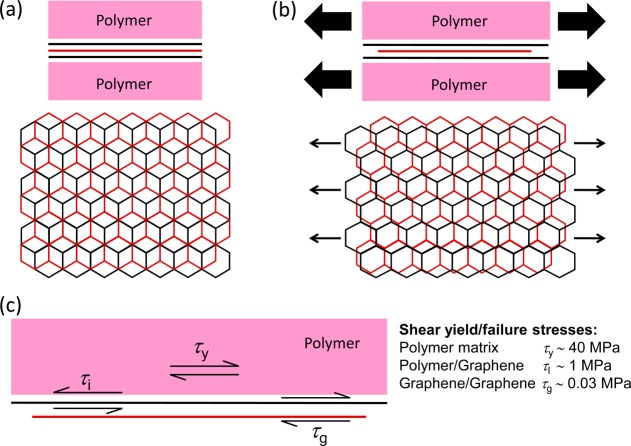
At this stage it is important to consider the process that must take place on the atomic level leading to the loss of Bernal stacking in the tri- and few-layer materials. The process is shown schematically in Figure 4 for a Bernal stacked trilayer graphene nanocomposite. When the polymer matrix is deformed, stress is transferred by interfacial stress transfer to the two outer graphene layers (both will be A-type layers) as has been found before for monolayer and bilayer specimens. They will become elongated in the tensile direction and narrower in the transverse direction due to Poisson contraction.31 Stress transfer to the inner B-type layer can only take place by shear from the two outer A-type layers. If this does not take place efficiently, then the two A-type outer layers will become deformed and the inner layer will remain relatively undeformed, as shown in Figure 4b. The consequence of this is that the Bernal stacking will be lost. On unloading the outer layers will revert to their original form and Bernal stacking will be regained. It is envisaged that a similar process will also occur for few-layer material investigated in this study. It should be noted that the Bernal stacking is not lost in the case of bilayer specimens as both graphene layers have interfaces with the polymer matrix that remain intact up to 0.4% strain.
Figure 4.
Schematic illustration of the loss of Bernal stacking during the deformation of trilayer graphene in a nanocomposite: (a) undeformed structure; (b) deformed structure showing the loss of Bernal stacking through affine deformation; (c) the shear process that take place at the different interfaces along with their values at yield or failure (the A layers are colored black and the B layer is colored red).
This stress transfer in composites takes place through shear at the interfaces between the different components24 as shown schematically for the nanocomposite in Figure 4c. Stress transfer will take place from the polymer matrix to the outer graphene layer and this is then transferred to the inner layers by shear between the outer graphene layer and the next layer as indicated. It has been found in a previous study26 that transfer between the inner graphene layers is no more than 70% efficient, leading to a reduction in effective Young’s modulus as the number of graphene layers is increased above two. In addition, the shear yield stresses for stress transfer at the different graphene interfaces are known from the literature as indicated in Table 1.
Table 1. Values of Shear Yield Stress and Interfacial Shear Stress for Interfacial Failure in Polymer–Graphene Nanocomposites.
It is clear from the table that the weakest interface is that between the inner graphene layers which in graphite fail at a shear stress of only τg ∼ 30 kPa.44 Investigations upon model monolayer graphene composites have shown that the shear stress for interfacial stress transfer between the graphene and the polymer is of the order of τi ∼ 1 MPa.24 Studies upon the mechanical properties of glassy polymers45 have shown that such materials have a shear yield stress of the order of τy ∼ 40 MPa so that the polymer matrix would be unlikely to undergo yielding in this system. Hence, it would be expected that the first interface to fail during the deformation of the few-layer graphene nanocomposites studied would be that between the inner graphene layers.
The loss of Bernal stacking shown in Figure 4b leads to the formation of a basal-plane stacking fault in the trilayer graphene. It is shown in the Supporting Information that this occurs at around 0.4% strain. The elastic strain energy released upon the unloading the inner graphene layer from this strain can be readily calculated and is found to be the order of 0.2 meV/atom (see Supporting Information).
Telling and Heggie42 have reviewed the literature upon stacking faults on the basal plane of graphite and pointed out that, although the binding energy from the van der Waals forces between the graphene layers is of the order of 35 meV/atom, the basal plane is prone to stacking faults and readily accommodates basal dislocations. They showed that the stacking fault energy in graphite varies with the geometry of the fault between as low as 0.11 meV/atom for ABC rhombohedral stacking to 9.7 meV/atom for AA simple hexagonal stacking. In a recent study, Shibuta and Elliott46 investigated the interaction between two graphene sheets with a turbostratic orientational relationship. They investigated the loss of AB stacking through either rotation or displacement of the two sheets relative to each other and the showed that in this case the energy gap between AB and AA stacking is only the order of 0.36 meV/atom. They also pointed out that, since this energy is much smaller than the average thermal energy at room temperature (kBT = 25.7 meV/atom), the two graphene sheets will have easy rotational and translational motion at room temperature.46 For example, Figure 3b shows a relative rotation of two graphene sheets that readily results from CVD growth. It is clear therefore that the elastic energy of 0.2 meV/atom released from the unloading of the inner graphene layer at around 0.4% strain is capable of leading to the loss of Bernal stacking in the few-layer graphene observed by Raman spectroscopy.
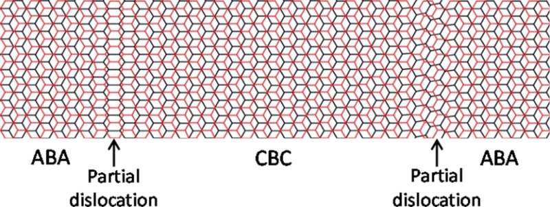
It is most likely that this loss of Bernal stacking in few-layer graphene will not occur through affine deformation (as shown in Figure 4) but would be accommodated by the formation of arrays of partial dislocations and stacking faults as was observed more than 50 years ago in the case of graphite.40,41 The situation is shown for trilayer material in Figure 5. The material with ABA Bernal stacking before deformation is shown in Figure 5a (the two outer A layers are assumed to deform equally and are thus identical). Figure 5b shows the situation during deformation with the middle B layer unloaded and two partial dislocations in each outer layer with a stacking fault between them. The fault will be of the CBC type (and hence still Bernal stacked) if identical dislocations form in both the top and bottom layers, or of the rhombohedral CBA type if only the top layer is deformed. The full development of the dislocations and stacking faults is shown in Figure S5 of the Supporting Information.
Figure 5.
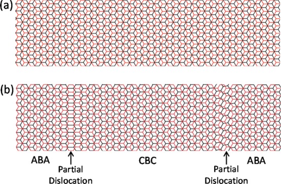
Bernal stacked trilayer graphene lattice structure. (a) undeformed material; (b) deformed structure showing an undeformed B layer and the formation of two partial dislocations and a stacking fault between them (the top and bottom A layers are shown identically with the same deformation for clarity). The left-hand side partial dislocation has edge character, and the right-hand side one is mixed edge and screw. The top and bottom (A stacked at edges and C stacked in stacking fault) layers are colored black and the middle layer (B stacked) is colored red.
It is possible to estimate the critical size of the partial dislocations in the few-layer material as shown in the Supporting Information. It is found that the width of the partial dislocation is expected to be of the order of 40 nm and their separation is also around 35 nm. For clarity, the dislocations shown schematically in Figure 5 have been given a width of only around 10 nm, by imposing a sinusoidal displacement. The calculation in the Supporting Information shows that in reality the partial dislocations will be much broader as a result of the low stacking fault energy and the whole area will effectively be faulted.
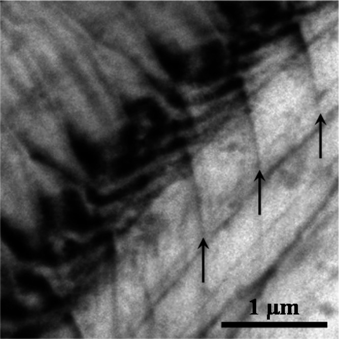
There is extensive literature upon the observation and analysis of basal plane dislocations and stacking faults in graphite by transmission electron microscopy. The best examples are as a result of radiation damage where extensive arrays of basal plane stacking faults bounded by partial dislocations are obtained.40,41 Since in our case the dislocations and stacking faults are only expected to be present during shear deformation, it is difficult to observe their formation in the transmission electron microscope. In addition, the contrast from such defects in few-layer graphene would be very weak. Figure 6 shows an array of dislocations and stacking faults in a relatively thick graphene flake (>20 layers) prepared by mechanical cleavage. The defects were induced during 60 keV Xe+ ion irradiation and the image contrast is consistent with a dislocation width of the order of 50 nm.
Figure 6.
Transmission electron micrograph showing dislocation arrays (dislocation lines indicated by arrows) in a many-layer graphene flake prepared by mechanical cleavage.
Bao et al. have recently investigated the stacking dependent band gap and quantum transport in trilayer graphene.20 They pointed out that the stacking order provides an extra degree of freedom for tuning its electronic properties. For example, Bernal stacked trilayer graphene is semimetallic with a tunable band overlap, whereas rhombohedral stacked graphene is predicted to be semiconducting with a tunable band gap. In particular, Bao et al. demonstrated that trilayer graphene with the two differ types of stacking has dramatically different transport properties.20 It would seem, therefore, that the demonstration in this present study of the possibility of reversibly disrupting the stacking sequence of tri- and few-layer graphene could have important implications for the use of the material in electronic applications.
Conclusions
It has been demonstrated that few-layer graphene undergoes a reversible loss of Bernal stacking upon shear deformation in nanocomposites. This behavior leads to a reduction in the effective Young’s modulus of the graphene that has been observed as the number of layers increases. It has been shown that the process can take place through the formation of arrays of partial dislocation and stacking faults between the graphene layers. As well as having major consequences for the mechanical properties of graphene nanocomposites, it is also likely that the phenomenon may lead to a method of reversibly modifying the electronic structure of few-layer graphene.
Methods
In this present study we have followed the effect of deformation upon the 2D band in the Raman spectra of a number of model nanocomposites consisting of exfoliated monolayer, bilayer, trilayer, and few-layer graphene flakes embedded in a polymer matrix on a poly(methyl methacrylate) (PMMA) beam. The flakes were sandwiched between thin layers of cured SU-8 (spin-coated to ∼300 nm thick). Full details of the specimen preparation and test procedures are given in the Supporting Information and elsewhere.24−26
The Raman spectra were excited using a 785 nm (1.59 eV) laser with a Renishaw 2000 Raman spectrometer and obtained from the middle of a number of different flakes on the PMMA beam, with a laser power at the sample of <1 mW. The beam was deformed in steps of ∼0.05 to 0.4% strain (monitored using a resistance stain gauge fixed to the beam) and then unloaded. Spectra were obtained from the central regions of each the flakes being monitored at each strain level.
The high resolution TEM images in Figure 3 were obtained using JEOL 2200MCO (S)TEM aberration corrected to third order and operated at an accelerating voltage of 80 kV. The TEM image in Figure 6 was obtained using a JEOL200FX TEM operated at 80 kV.
Acknowledgments
The authors of this work are grateful to the Engineering and Physical Sciences Research Council for support in the form of a Science and Innovation Award (EP/G035954/1). One of the authors (K.S.N.) is also supported by the Royal Society.
Supporting Information Available
Details of specimen preparation; full details of the dependence of the 2D band position upon strain for monolayer, bilayer, trilayer, and few-layer graphene; schematic illustration of straining of the trilayer graphene lattice leading to the loss of Bernal stacking and calculations of the energetics of formation of the dislocations and stacking faults. This material is available free of charge via the Internet at http://pubs.acs.org.
The authors declare no competing financial interest.
Supplementary Material
References
- Geim A. K.; Novoselov K. S. The Rise of Graphene. Nat. Mater. 2007, 6, 183–191. [DOI] [PubMed] [Google Scholar]
- Novoselov K. S.; Geim A. K.; Morozov S. V.; Jiang D.; Zhang Y.; Dubonos S. V.; Grigorieva I. V.; Firsov A. A. Electric Field Effect in Atomically Thin Carbon Films. Science 2004, 306, 666–669. [DOI] [PubMed] [Google Scholar]
- Novoselov K. S.; Jiang D.; Schedin F.; Booth T. J.; Khotkevich V. V.; Morozov S. V.; Geim A. K. Two-Dimensional Atomic Crystals. Proc. Natl. Acad. Sci. U.S.A. 2005, 102, 10451–10453. [DOI] [PMC free article] [PubMed] [Google Scholar]
- Novoselov K. S.; Geim A. K.; Morozov S. V.; Jiang D.; Katsnelson M. I.; Grigorieva I. V.; Dubonos S. V.; Firsov A. A. Two-Dimensional Gas of Massless Dirac Fermions in Graphene. Nature 2005, 438, 197–200. [DOI] [PubMed] [Google Scholar]
- Lee C.; Wei X. D.; Kysar J. W.; Hone J. Measurement of the Elastic Properties and Intrinsic Strength of Monolayer Graphene. Science 2008, 321, 385–388. [DOI] [PubMed] [Google Scholar]
- Kelly A.; Macmillan N. H.. Strong Solids, 3rd ed.; Clarendon Press: Oxford, 1986. [Google Scholar]
- Bernal J. D. The Structure of Graphite. Proc. R. Soc. A 1924, 106, 749–773. [Google Scholar]
- McCann E.; Fal’ko V. I. Landau-Level Degeneracy and Quantum Hall Effect in a Graphite Bilayer. Phys. Rev. Lett. 2006, 96, 086805. [DOI] [PubMed] [Google Scholar]
- Brown L.; Hovden R.; Huang P.; Wojcik M.; Muller D. A.; Park J. Twinning and Twisting of Tri- and Bilayer Graphene. Nano Lett. 2012, 12, 1609–1615. [DOI] [PubMed] [Google Scholar]
- Shallcross S.; Sharma S.; Landgraf W.; Pankratov O. Electronic Structure of Graphene Twist Stacks. Phys. Rev. B 2011, 83, 153402. [Google Scholar]
- Mele E. J. Band Symmetries and Singularities in Twisted Multilayer Graphene. Phys. Rev. B 2011, 84, 235439. [Google Scholar]
- Hicks J.; Sprinkle M.; Shepperd K.; Wang F.; Tejeda A.; Taleb-Ibrahimi A.; Bertran F.; Le F̀ever P.; de Heer W. A.; Berger C.; et al. Symmetry Breaking in Commensurate Graphene Rotational Stacking: Comparison of Theory and Experiment. Phys. Rev. B 2011, 83, 205403. [Google Scholar]
- Warner J. H.; Rümmeli M. H.; Gemming T.; Büchner B.; Briggs G. A. D. Direct Imaging of Rotational Stacking Faults in Few Layer Graphene. Nano Lett. 2009, 9, 102–106. [DOI] [PubMed] [Google Scholar]
- Robertson A. W.; Bachmatiuk A.; Wu Y. A.; Schäffel F.; Büchner B.; Rümmeli M. H.; Warner J. H. Structural Distortions in Few-Layer Graphene Creases. ACS Nano 2011, 5, 9984–9991. [DOI] [PubMed] [Google Scholar]
- Zan R.; Bangert U.; Ramasse Q.; Novoselov K. S. Imaging of Bernal Stacked and Misoriented Graphene and Boron Nitride: Experiment and Simulation. J. Micros. 2011, 244, 152–158. [DOI] [PubMed] [Google Scholar]
- Tiberj A.; Camara N.; Godignon P.; Camassel J. Micro-Raman and Micro-transmission Imaging of Epitaxial Graphene Grown on the Si and C Faces of 6H-SiC. Nanoscale Res. Lett. 2011, 6, 478. [DOI] [PMC free article] [PubMed] [Google Scholar]
- Poncharal P.; Ayari A.; Michel T.; Sauvajol J.-L. Raman Spectra of Misoriented Bilayer Graphene. Phys. Rev. B 2008, 78, 113407. [Google Scholar]
- Lui C. H.; Li Z. Q.; Chen Z. Y.; Klimov V.; Brus L. E.; Heinz T. F. Imaging Stacking Order in Few-Layer Graphene. Nano Lett. 2011, 11, 164–169. [DOI] [PubMed] [Google Scholar]
- Cong C. X.; Yu T.; Sato K.; Shang J. Z.; Saito R.; Dresselhaus G. F.; Dresselhaus M. S. Raman Characterization of ABA- and ABC-Stacked Trilayer Graphene. ACS Nano 2011, 5, 8760–8768. [DOI] [PubMed] [Google Scholar]
- Bao W.; Jing L.; Velasco J. Jr.; Lee Y.; Liu G.; Tran D.; Standley B.; Aykol M.; Cronin S. B.; Smirnov D.; et al. Stacking-Dependent Band Gap and Quantum Transport in Trilayer Graphene. Nat. Phys. 2011, 7, 948–952. [Google Scholar]
- Mak K. F.; Shan J.; Heinz T. F. Electronic Structure of Few-Layer Graphene: Experimental Demonstration of Strong Dependence on Stacking Sequence. Phys. Rev. Lett. 2010, 104, 176404. [DOI] [PubMed] [Google Scholar]
- Latil S.; Meunier V.; Henrard L. Massless Fermions in Multilayer Graphitic Systems with Misoriented Layers: Ab initio Calculations and Experimental Fingerprints. Phys. Rev. B 2007, 76, 201402R. [Google Scholar]
- Luican A.; Li G. H.; Reina A.; Kong J.; Nair R. R.; Novoselov K. S.; Geim A. K.; Andrei E. Y. Single-Layer Behavior and Its Breakdown in Twisted Graphene Layers. Phys. Rev. Lett. 2011, 106, 126802. [DOI] [PubMed] [Google Scholar]
- Gong L.; Kinloch I. A.; Young R. J.; Riaz I.; Jalil R.; Novoselov K. S. Interfacial Stress Transfer in a Graphene Monolayer Nanocomposite. Adv. Mater. 2010, 22, 2694–2697. [DOI] [PubMed] [Google Scholar]
- Young R. J.; Gong L.; Kinloch I. A.; Riaz I.; Jalil R.; Novoselov K. S. Strain Mapping in a Graphene Monolayer Nanocomposite. ACS Nano 2011, 5, 3079–3084. [DOI] [PubMed] [Google Scholar]
- Gong L.; Young R. J.; Kinloch I. A.; Riaz I.; Jalil R.; Novoselov K. S. Optimizing the Reinforcement of Polymer-Based Nanocomposites by Graphene. ACS Nano 2012, 6, 2086–2095. [DOI] [PubMed] [Google Scholar]
- Ferrari A. C.; Meyer J. C.; Scardaci V.; Casiraghi C.; Lazzeri M.; Mauri F.; Piscanec S.; Jiang D.; Novoselov K. S.; Roth S.; et al. Raman Spectrum of Graphene and Graphene Layers. Phys. Rev. Lett. 2006, 97, 187401. [DOI] [PubMed] [Google Scholar]
- Malard L. M.; Pimenta M. A.; Dresselhaus G.; Dresselhaus M. S. Raman Spectroscopy in Graphene. Phys. Rep. 2009, 473, 51–87. [Google Scholar]
- Hao Y. F.; Wang Y. Y.; Wang L.; Ni Z. H.; Wang Z. Q.; Wang R.; Koo C. K.; Shen Z. X.; Thong J. T. L. Probing Layer Number and Stacking Order of Few-Layer Graphene by Raman Spectroscopy. Small 2010, 6, 195–200. [DOI] [PubMed] [Google Scholar]
- Huang M. Y.; Yan H.; Chen C. Y.; Song D. H.; Heinz T. F.; Hone J. Phonon Softening and Crystallographic Orientation of Strained Graphene Studied by Raman Spectroscopy. Proc. Natl. Acad. Sci. U.S.A. 2009, 106, 7304–7308. [DOI] [PMC free article] [PubMed] [Google Scholar]
- Mohiuddin T. M. G.; Lombardo A.; Nair R. R.; Bonetti A.; Savini G.; Jalil R.; Bonini N.; Basko D. M.; Galiotis C.; Marzari N.; et al. Uniaxial Strain in Graphene by Raman spectroscopy: G Peak Splitting, Gruneisen Parameters, and Sample Orientation. Phys. Rev. B 2009, 79, 205433. [Google Scholar]
- Metzger C.; Remi S.; Liu M.; Kusminskiy S. V.; Castro Neto A. H.; Swan A. K.; Goldberg B. B. Biaxial Strain in Graphene Adhered to Shallow Depressions. Nano Lett. 2009, 10, 6–10. [DOI] [PubMed] [Google Scholar]
- Ferralis N. Probing Mechanical Properties of Graphene with Raman Spectroscopy. J. Mater. Sci. 2010, 45, 5135–5149. [Google Scholar]
- Huang M. Y.; Yan H.; Heinz T. F.; Hone J. Probing Strain-Induced Electronic Structure Change in Graphene by Raman Spectroscopy. Nano Lett. 2010, 10, 4074–4079. [DOI] [PubMed] [Google Scholar]
- Mohr M.; Maultzsch J.; Thomsen C. Splitting of the Raman 2D Band of Graphene Subjected to Strain. Phys. Rev. B 2010, 82, 201409. [Google Scholar]
- Frank O.; Mohr M.; Maultzsch J.; Thomsen C.; Riaz I.; Jalil R.; Novoselov K. S.; Tsoukleri G.; Parthenios J.; Papagelis K.; et al. Raman 2D-Band Splitting in Graphene: Theory and Experiment. ACS Nano 2011, 5, 2231–2239. [DOI] [PubMed] [Google Scholar]
- Cheng Y. C.; Zhu Z. Y.; Huang G. S.; Schwingenschlögl U. Gruneisen Parameter of the G Mode of Strained Monolayer Graphene. Phys. Rev. B 2011, 83, 115449. [Google Scholar]
- Frank O.; Tsoukleri G.; Riaz I.; Papagelis K.; Parthenios J.; Ferrari A. C.; Geim A. K.; Novoselov K. S.; Galiotis C. Development of a Universal Stress Sensor for Graphene and Carbon Fibres. Nat. Commun. 2011, 2, 255. [Google Scholar]
- Frank O.; Bouša M.; Riaz I.; Jalil R.; Novoselov K. S.; Tsoukleri G.; Parthenios J.; Kavan L.; Papagelis K.; Galiotis C. Phonon and Structural Changes in Deformed Bernal Stacked Bilayer Graphene. Nano Lett. 2012, 12, 687–693. [DOI] [PubMed] [Google Scholar]
- Amelinckx S.; Delavignette P. Electron Optical Study of Basal Dislocations in Graphite. J. Appl. Phys. 1960, 31, 2126–2135. [Google Scholar]
- Baker C.; Kelly A. The Effect of Neutron Irradiation on the Elastic Moduli of Graphite Single Crystals. Philos. Mag. 1964, 9, 927–951. [Google Scholar]
- Telling R. H.; Heggie M. I. Stacking Fault and Dislocation Glide on the Basal Plane of Graphite. Philos. Mag. Lett. 2003, 83, 5122–5139. [Google Scholar]
- Tan P. H.; Han W. P.; Zhao W. J.; Wu Z. H.; Chang K.; Wang H.; Wang Y. F.; Bonini N.; Marzari N.; Pugno N.; et al. The Shear Mode of Multilayer Graphene. Nat. Mater. 2012, 11, 294–300. [DOI] [PubMed] [Google Scholar]
- Soule D. E.; Nezbeda C. W. Direct Basal-Plane Shear in Single-Crystal Graphite. J. Appl. Phys. 1968, 39, 5122–5139. [Google Scholar]
- Yamini S.; Young R. J. The Mechanical Properties of Epoxy Resins 1. Mechanisms of Plastic-Deformation. J. Mater. Sci. 1980, 15, 1814–1822. [Google Scholar]
- Shibuta Y.; Elliott J. A. Interaction between Two Graphene Sheets with a Turbostratic Orientational Relationship. Chem. Phys. Lett. 2011, 512, 146–150. [Google Scholar]
Associated Data
This section collects any data citations, data availability statements, or supplementary materials included in this article.


