Abstract
Complementary resistive switches based on two anti-serially connected Ag/GeSx/Pt devices were studied. The main focus was placed on the pulse mode properties as typically required in memory and logic applications. A self-designed measurement setup was applied to access each CRS part-cell individually. Our findings reveal the existence of two distinct read voltage regimes enabling both spike read as well as level read approaches. Furthermore, we experimentally verified the theoretically predicted kinetic properties in terms of pulse height vs. switching time relationship. The results obtained by this alternative approach allow a significant improvement of the basic understanding of the interplay between the two part-cells in a complementary resistive switch configuration. Furthermore, from these observations we can deduce a simplified write voltage scheme which is applicable for the considered type of memory cell.
Redox-based resistively switching devices (ReRAM) are considered appropriate elements to boost performance in future nanoelectronics as non-volatile memories and beyond-CMOS logic applications1,2,3,4. ReRAM cells offer ultimate scalability5,6, fast operation speed and high energy efficiency and are capable to replace both, DRAM and FLASH memory technologies1. Various materials e.g. oxides and higher chalcogenides have been studied as solid electrolytes. Ag-GeSx-based cells already proved to be a strong candidate for well working resistive memory devices7,8,9,10,11,12,13,14. Furthermore, unconventional computing approaches, which enable multi-parallel computing, are feasible by utilizing these novel devices in passive crossbar arrays15,16,17.
The main concern of the implementation of passive crossbar arrays is the inherent selection device issue which is also reflected by a new section of the ITRS' ERD roadmap1: Either a bipolar rectifying element18,19 or the recently introduced complementary resistive switch (CRS) paradigm20 can be used to overcome the “sneak path problem”. The sneak path problem occurs in resistive switch-based passive crossbar arrays due to a lack of cell isolation, which leads to large parasitic currents. To avoid these parasitic currents a selector device is required in general20. In terms of CRS, two anti-serially connected ReRAM cells act as combined selector and storing element. Most recent research activities have concentrated on material engineering and basic quasi-static I-V characterizations of the CRS devices21,22,23,24. However, studying CRS devices in pulse mode is much more appropriate and in fact is essential to explore the feasibility for memory and logic applications and to obtain a deeper understanding of the device dynamics under real operation conditions.
In Figure 1, the generic quasi-static properties of ECM-based complementary resistive switches are shown. To obtain stable ON windows a series resistor is required to be introduced due to an asymmetry in SET and RESET device voltages20. In terms of voltage division the additional series resistor's purpose is to take over a certain part of the voltage in the ON state (LRS/LRS), and thus effectively prevents a direct switching from HRS/LRS to LRS/HRS. In Figure 1a, the typical current response to a triangular quasi-static voltage sweep is depicted. Initially, the top cell A is in HRS and cell B in LRS. First, the CRS device switches to LRS/LRS at the first threshold voltage Vth,1, and when reaching Vth,2, the CRS device switches further to LRS/HRS. Similarly, when coming to negative voltages, the CRS device switches to LRS/LRS at Vth,3 and back to HRS/LRS at Vth,4. For comparison, the same cycle is shown in Figure 1b without the application of a series resistor. Correspondingly, the LRS/LRS is not stable and only a transient current increase (a current spike) occurs. Thus, the absence of a large enough series resistor seems to make a level read operation impossible. We demonstrate that it is anyhow possible to perform a level read by selection of appropriate pulsed signals.
Figure 1. CRS I-V behaviour for excitation by a quasi-static triangular voltage sweep.
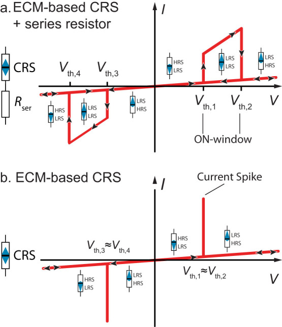
(a) ECM-based CRS device with series resistor. In the ON-window a relevant voltage drop is taken over by the series resistor. (b) ECM-based CRS device without series resistor. Due to SET/RESET asymmetry of ECM cells (e.g., VSET = 0.2 V and VRESET < −0.05 V), a RESET of the second CRS part cell B occurs directly after SET of the first part cell A.
Since the ECM cells are asymmetric in terms of SET and RESET voltage (VRESET < VSET/2) as depicted in Figure 1b, it is not trivial to observe the basic switching operation of the CRS memory device during voltage sweeps due to the limited time resolution of the used sourcemeter. Short current spikes, as expected from theory, cannot be recorded. Therefore, common two-point quasi-static I-V measurements of CRS devices are not feasible and a significantly improved setup as shown as an inset in Figure 2 is required. The dual-channel sourcemeter was connected to the active electrodes of the cells A and B to apply the voltages to the CRS device. At the same time the voltage between the middle electrode and the active electrode of cell B was measured to gain information about the particular status of memory cells A and B, respectively. Note, that for proper CRS operation within passive crossbar arrays, a connection to the middle electrode is not required.
Figure 2. CRS voltage sweep (sweep rate: 1 V/s) depicting the voltages over the individual memory cells A and B normalized to VCRS.
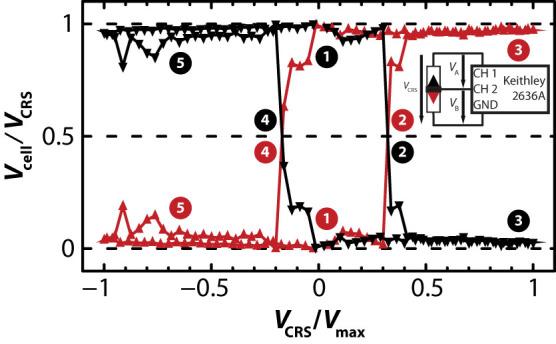
VCRS is applied to the whole device and the individual voltage drops VA and VB of each part-cell are accessible via the middle electrode contact.
Figure 2 depicts the typical voltage characteristics of the individual memory cells (normalized to the voltage over the full CRS device) in the course of a voltage sweep. The CRS device's memory cell A was set to an HRS and memory cell B was set to an LRS prior to the measurements, as described in the method section. The voltage sweep started at 0 V, continued to Vmax, then was returned back to − Vmax and ended again at 0 V. Immediately after the start of the sweep the voltage distribution over the individual cells clearly proved their initial status (A: HRS, B: LRS). The high voltage ratio (Vcell/VCRS approx. 1) corresponds to an HRS and the low voltage ratio (Vcell/VCRS approx. 0) corresponds to an LRS (see Figure 2, (1)). As the sweep continues further, there is a switch-over of the whole CRS device observed at point (2). Memory cell A switches from an HRS to an LRS and memory cell B switches from an LRS to an HRS, leaving the CRS device in a reversed configuration that is stable during the following positive part of the voltage sweep (see (3)). The configuration of the CRS device was reversed again not until the negative part of the sweep at point (4) was reached. Here memory cell A switches from an LRS back to the initial HRS and memory cell B switches from an HRS back to the initial LRS (see (5)). Thereby, we prove the basic functionality of the GeSx-based CRS device during voltage sweeps. Most importantly, by this quasi-static measurement we demonstrated the predicted basic characteristic as shown in Figure 1b that is due to the SET/RESET asymmetry (VRESET < VSET/2). It is noteworthy that this behaviour can also be observed when, like in our case, cells with slightly differing electrolyte dimensions and differing line resistances are used, which results in shifted threshold voltages (Vth,3,4 = −0.15 V and Vth,1,2 = 0.35 V). For obtaining more details at operation mode relevant experimental conditions we used pulse measurements for basic read and write operations as well as resulting array constraints. The pulse mode operation reveals some unique features of this system being highly application-relevant:
large ON-windows for level read in a fast pulse regime
an easy-to-access spike read procedure
the feasibility of half-select array write schemes
Furthermore, we experimentally verified the theoretically derived pulse height vs. switching time dependence as predicted in25.
For proper write operation, a voltage larger than Vth,2 and Vth,4, respectively, is required. A direct constraint in terms of passive array operation is to not disturb non-accessed cells of the array. Therefore, the voltage drop at non-accessed cells must not exceed Vth,1 to prevent these cells from unintentionally switching. To obtain the required safety margins, either a half select (Figure 3a) or a third-select (Figure 3b) scheme can be applied. However, there is a specific trade-off for CRS devices: On the one hand a large ON window is desirable to have a large safety margin for level read, but on the other hand a sufficiently large ON-window necessitates a one-third write scheme, as depicted in Figure 3c. In that case a half select scheme would result in a half select voltage larger than Vth,1, thus non-accessed cells would switch.
Figure 3.

(a) In the half voltage select scheme, the full voltage V is applied to the device which is to be written (here: upper left element). To prevent non-accessed elements from switching, half of the voltage is applied to the other lines. Thus, voltage drop at non-accessed elements is either 1/2 V or 0 V. (b) In the third voltage select scheme, non-access columns offer 1/3 V while non-access rows offer 2/3 V. Thus, the maximum voltage drop at non-accessed elements is |1/3 V|. (c) The impact of applied write schemes on array safety margins is visualized here. For a half-select scheme non-accessed elements see a voltage larger than Vth,1, and therefore would switch to LRS/LRS. To avoid this unintentional switching for CRS offering large ON-windows, a third voltage scheme is required.
In conclusion, for readout it would be preferable to have a device offering a large ON-window, e.g. an ECM-based CRS device plus series resistor (compare Figure 1a), while in terms of applicable write scheme and corresponding margins, a CRS with no ON-window, e.g. an ECM-based CRS device without series resistor (compare Figure 1b), is desired. This trade-off is controllable when using ECM-based CRS in pulse mode without the need for any series resistor.
Results
Pulsed switching with middle electrode
To study the switching operation of the memory cells inside a CRS device, we used the measurement setup illustrated in the inset of Figure 4. The current through the device ICRS was observed over a 50 Ω series resistance of the oscilloscope. We applied 50 μs pulsed voltages Vpulse of +2 V and −2 V respectively to the test setup that are high enough to allow a stable switching operation and low enough to allow a detailed observation of the switching process. From the measured voltages Vpulse, Vmiddle and VI all relevant voltages and currents can be derived:
Figure 4 gives a detailed overview of the sequence of the voltage VCRS, the observed voltage VB over memory cell B and the corresponding resistances RA and RB of memory cells A and B, respectively. VCRS was smaller than the applied voltage due to the voltage drop over the series resistor that was especially predominant when the memory cells of the CRS device were both in an LRS state. The presented measurements started with both memory cells in an LRS. By applying a negative voltage pulse to the CRS device, memory cell A was switched to an HRS. A second negative pulse verified that the switching was successful. Then a series of positive voltage pulses was applied and at first memory cell A switched back to an LRS and consecutively memory cell B switched to an HRS. Finally the CRS device was switched back to its initial state with both memory cells in an LRS by applying a negative voltage pulse. This measurement sequence clearly shows the effective implementation of the CRS concept to GeSx-based ECM memory cells.
Figure 4. CRS switching sequence during pulsed measurements.
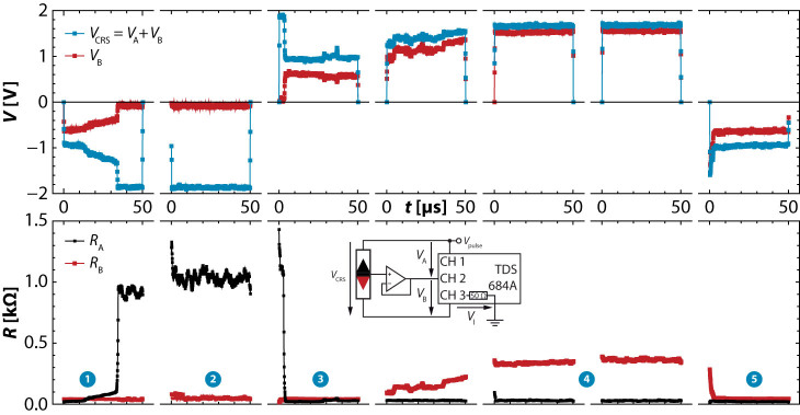
1. (A): LRS, (B): LRS 2. (A): HRS, (B): LRS 3. (A): LRS, (B): LRS 4. (A): LRS, (B): HRS 5. (A): LRS, (B): LRS.
Read regimes
The measurements up to now were focused mainly on a full switch-over of the CRS device, changing the resistance of both used memory cells from either HRS to LRS or LRS to HRS. In the level read regime only one of the two memory cells is stressed during the reading process. However, this readout procedure is not available in quasi-static mode for ECM-based CRS devices, compare Figure 1b. To examine the level read capabilities of ECM-based CRS memory devices we used again our measurement setup with a series resistance of 50 Ω (see Figure 7b of the methods section), what is well below the lowest LRS. We applied positive voltage pulses in the range of 2 to 5 V to a selected memory device, where memory cell A was in an LRS and memory cell B was in an HRS. The current response was then analysed to extract the time from the rising edge of the voltage pulse until the rising edge of the current peak, i.e. the set time tSET, and furthermore until the falling edge of the current peak, i.e. the reset time tRESET. All three points were extracted at half maximum of each pulse's edges. As can be seen from Figure 5 there is a notable variation of set and reset times in our GeSx-based CRS devices. For application as memory devices this variability must be reduced by materials and/or cell design to avoid read failures. Despite these statistical variations of the measurement data we clearly observe that at voltages below 4 V the reset time tRESET is at the average significantly longer than the set time tSET. For voltages above 4 V the set times are still shorter than the reset times, but both move to the same dimension and their values stabilize (see Figure 5). Dynamic physics-based simulations predicted this behaviour specific to ECM memory cells as can be seen from the inset in Figure 525.
Figure 5. CRS level-read behaviour for different pulse voltages Vpulse.
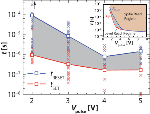
There are three regimes which can be distinguished with respect to pulse height and pulse duration. For pulses below the red line, no change of the resistive state, i.e. no SET of the high resistive part-cell, occurs. In the regime between the red and blue curve, one part-cell is switched from HRS to LRS, leading to the overall conductive LRS/LRS state. This operation is required for level read. In the regime above the blue line, a full switch-over of the CRS device occurs, thus pulses in this regime can be used for a spike read operation. Inset: level-read behaviour as predicted by specific ECM memory cell dynamic physics-based simulations25.
Figure 6.
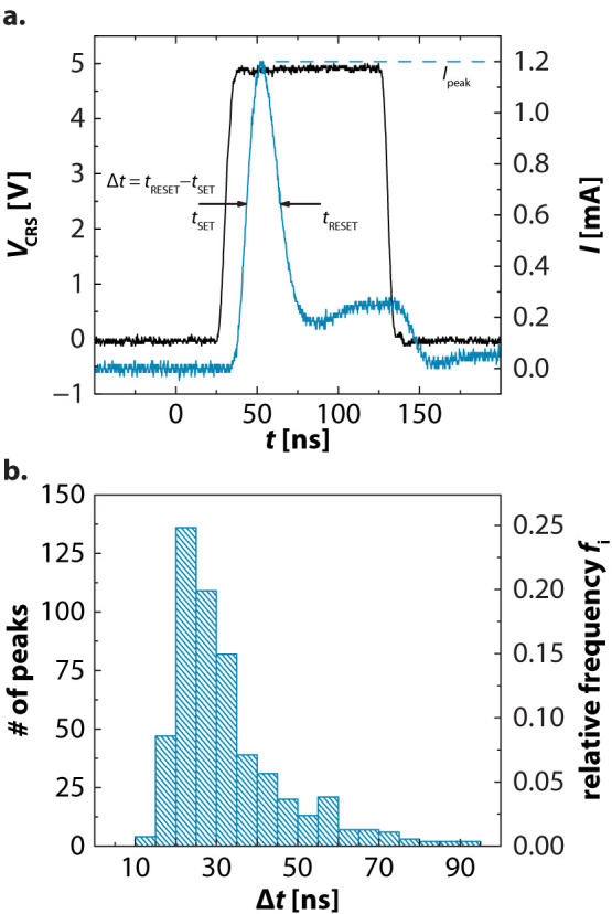
Switching time of an ECM CRS device (a) General pulse response of an CRS device. (b) Statistical evaluation of the switching action during fast pulse measurements.
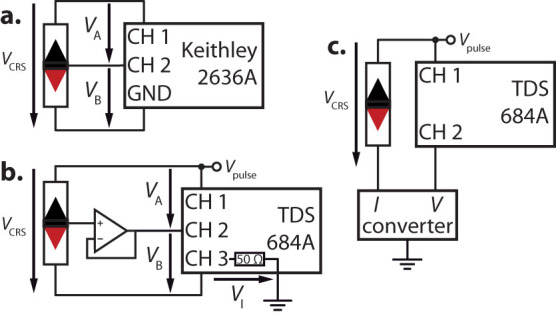
Figure 7. Measurement circuits (a) IV-sweeps (b) fast pulse measurements with series resistor (c) fast pulse measurements with IV-converter.
For the targeted memory applications, a fast pulse operation mode is required. Figure 6 summarizes the switching properties of a CRS device for short voltage pulses measured with the setup shown in Figure 7c. In previous measurements we were able to confirm that the typical switching time for a single GeSx-based ECM cell can be well below 100 ns even for crossbars in the micrometre range, which is another strong reference to the filamentary nature of the ECM switching mechanism. For that reason, the pulse length was set to 100 ns and smaller values in order to achieve a satisfying time resolution of the expected current spike. The pulse voltage was set alternately to 5 V and −5 V. Figure 6a depicts a typical current response when we applied a positive voltage pulse to a CRS device. The current spike exhibits a width at half maximum of about 22.4 ns. In general a delay of the current response of about 15 ns can be attributed to the current-to-voltage-converter. Taking this into account, the time to SET is in the range of 20–30 ns. The LRS/HRS resistance of the whole CRS device was about 20 kΩ.
In Figure 6b the current spike widths are summarized in form of a histogram. Nearly 50% of the current peaks are shorter than 30 ns. The time for a full switch over of a CRS device could possibly be further decreased, for example, by decreasing the thickness of the GeSx layer or smaller RC times by reducing the electrode area.
Discussion
It is clearly shown by our results that Germanium-Sulphide-based ECM memory cells are suitable for integration in CRS devices. GeSx-based CRS devices exhibit ultra-fast switching in the range of 20 ns. The clear current response in pulse operation mode demonstrates impressively the application of the spike read method. Furthermore, we demonstrated the beforehand simulated behaviour of a CRS device in combination with a series resistor and confirmed the possibility of the level read method. The switching kinetics of this type of CRS devices enables, mainly due to the SET/RESET asymmetry, the implementation of a technically less challenging half select scheme during operation.
Methods
Preparation
The prototypical CRS devices in this study were manufactured as two separate anti-serially connected Ag/GeSx/Pt (being Ag the active and Pt the inert electrode) electrochemical metallization cells (ECM)26 with an accessible common middle electrode. The middle electrode was produced as a 50 nm thick and 2 μm wide Pt finger, acting as the inert electrode in the two ECM cells. The active electrodes were fabricated as 50 nm thick and 2 μm wide Ag fingers perpendicular to the middle electrode, resulting in a cross-point area of 4 μm2. The Ag electrodes were covered with a 50 nm film of Pt for protection. A sputtered 70 nm thin-film of GeSx with an S to Ge ratio of 2.2 was used as the solid electrolyte between the middle electrode and the two active electrodes and produced according to the procedures published before27. Ion beam etching was used to structure the middle electrode at the bottom of the stacks, whereas the contact hole in the GeSx thin-film and the topmost active electrodes were structured by a lithographical lift-off process.
Electrical characterization
After fabrication of the CRS device both memory cells are in a very high HRS in the GΩ-range and need a forming step to be operational. The general procedure to initialize the CRS device is to apply several positive voltage sweeps to switch memory cell B to an LRS and subsequently several negative voltage sweeps to switch memory cell A to an LRS and memory B to an HRS. This is the initial configuration for our measurements. Note that during CRS operation the initial HRS/HRS state cannot be regained and either HRS/LRS or LRS/HRS is available by applying write voltages.
All measurements were performed in a four-needle electrode microprobe station equipped with coaxial probes, micromanipulators to contact the electrodes and an optical microscope. A dual-channel Keithley 2636A SourceMeter was used for the current-voltage (IV) measurements (see Figure 7a). The pulse measurements were conducted in the same probe station and a Wavetek 395 100 MHz Arbitrary Waveform Generator was used to generate the pulses. For the high speed voltage measurements a Tektronix TDS 684A oscilloscope was used with input impedance set to 50 Ω.
For the voltage sensing at the middle electrode of a CRS device a custom-build active probe based on an impedance converter was designed. Common oscilloscope active probes have input impedances as high as 1 MΩ, which would represent a non-negligible leakage for the resistive cells. In order not to add an additional current path with a resistance lower than the parallel memory cell resistance, the input of the sensing probe must feature a high input impedance. An Analog Devices ADA4817-1 FET-Input type operational amplifier with 1 GHz bandwidth was employed. The input impedance of the active probe is 500 GΩ and its input capacitance is close to 1 pF what ensures a sufficient decoupling from the CRS device. This method ensures flawless voltage readout without any influence on the CRS device's operation and behaviour. (See Figure 7b).
The current-to-voltage converter is a two stage transimpedance amplifier with a negligible voltage drop over the circuitry and a transimpedance gain of 260 (see Figure 7c). Current measurements over a series resistor were performed by using the oscilloscope's internal 50 Ω resistor. (See Figure 7a).
Author Contributions
J.v.d.H. and E.L. conceived and designed the measurements. J.v.d.H. supervised the sample preparation and the measurements. V.H. contributed to the measurement equipment. R.W. and I.V. supervised the research. All authors discussed the results and contributed to the writing of the manuscript.
Acknowledgments
The authors would like to thank Robin Reckmann for sample preparation and measurements and Adesto Technologies for fruitful discussions and cooperation. The work was financially supported in part by SFB 917 Nanoswitches.
References
- ITRS, The International Technology Roadmap for Semiconductors - ITRS 2011 Edition. (2011).
- Yang J. J., Strukov D. B. & Stewart D. R. Memristive devices for computing. Nat. Nanotechnol. 8, 13–24 (2013). [DOI] [PubMed] [Google Scholar]
- Waser R., Dittmann R., Staikov G. & Szot K. Redox-Based Resistive Switching Memories - Nanoionic Mechanisms, Prospects, and Challenges. Adv. Mater. 21, 2632–2663 (2009). [DOI] [PubMed] [Google Scholar]
- Hasegawa T., Terabe K., Tsuruoka T. & Aono M. Atomic Switch: Atom/Ion Movement Controlled Devices for Beyond Von-Neumann Computers. Adv. Mater. 24, 252–267 (2012). [DOI] [PubMed] [Google Scholar]
- Terabe K., Hasegawa T., Nakayama T. & Aono M. Quantized conductance atomic switch. Nature 433, 47–50 (2005). [DOI] [PubMed] [Google Scholar]
- Valov I. et al. Atomically controlled electrochemical nucleation at superionic solid electrolyte surfaces. Nat. Mater. 11, 530–535 (2012). [DOI] [PubMed] [Google Scholar]
- Murugesan S., Kearns P. & Stevenson K. J. Electrochemical Deposition of Germanium Sulfide from Room-Temperature Ionic Liquids and Subsequent Ag Doping in an Aqueous Solution. Langmuir 28, 5513–5517 (2012). [DOI] [PubMed] [Google Scholar]
- Jameson J. R. et al. Quantized Conductance in Ag/GeS2/W Conductive-Bridge Memory Cells. IEEE Electron Device Lett. 33, 257–259 (2012). [Google Scholar]
- Lin S. et al. Electrochemical Simulation of Filament Growth and Dissolution in Conductive-Bridging RAM (CBRAM) with Cylindrical Coordinates. 2012 IEEE International Electron Devices Meeting (IEDM). 26.3.1–26.3.4 (2012). [Google Scholar]
- Cho D.-Y., Valov I., Tappertzhofen S., van den Hurk J. & Waser R. Spectroscopic investigation of charge transfer in electrochemical metallization memory cells. Technical Digest of Frontiers in Electronic Materials, Wiley-VCH, 213 (2012). [Google Scholar]
- Vianello E. et al. Sb-doped GeS2 as performance and reliability booster in Conductive Bridge RAM. 2012 IEEE International Electron Devices Meeting (IEDM). 31.5.1–31.5.4 (2012). [Google Scholar]
- Valov I. et al. Nanobatteries in redox-based resistive switches require extension of memristor theory. Nature Communications 4, 1771 (2013). [DOI] [PMC free article] [PubMed] [Google Scholar]
- Menzel S. et al. Simulation of polarity independent RESET in electrochemical metallization memory cells. 2013 5th IEEE International Memory Workshop (IMW). 92–95 (2013). [Google Scholar]
- Vianello E. et al. On the impact of Ag doping on performance and reliability of GeS2-based Conductive Bridge Memories. ESSDERC 2012 - 42nd European Solid State Device Research Conference, 278–281 (2012). [Google Scholar]
- Di Ventra M. & Pershin Y. V. The parallel approach. Nat. Phys. 9, 200–202 (2013). [Google Scholar]
- Borghetti J. et al. ‘Memristive’ switches enable ‘stateful’ logic operations via material implication. Nature 464, 873–876 (2010). [DOI] [PubMed] [Google Scholar]
- Likharev K. K. CrossNets: Neuromorphic Hybrid CMOS/Nanoelectronic Networks. Science of Advanced Materials 3, 322–331 (2011). [Google Scholar]
- Puthentheradam S. C., Schroder D. K. & Kozicki M. N. Inherent diode isolation in programmable metallization cell resistive memory elements. Appl. Phys. A - Mater. Sci. Process. 102, 817–826 (2011). [Google Scholar]
- Lee W. et al. High Current Density and Nonlinearity Combination of Selection Device Based on TaOx/TiO2/TaOx Structure for One Selector–One Resistor Arrays. ACS Nano 6, 8166–8172 (2012). [DOI] [PubMed] [Google Scholar]
- Linn E., Rosezin R., Kügeler C. & Waser R. Complementary Resistive Switches for Passive Nanocrossbar Memories. Nat. Mater. 9, 403–406 (2010). [DOI] [PubMed] [Google Scholar]
- Wouters D. J. et al. Analysis of Complementary RRAM Switching. IEEE Electron Device Lett. 33, 1186–1188 (2012). [Google Scholar]
- Schmelzer S., Linn E., Böttger U. & Waser R. Uniform Complementary Resistive Switching in Tantalum Oxide Using Current Sweeps. IEEE Electron Device Lett. 34, 114–116 (2013). [Google Scholar]
- Tang G. et al. Programmable complementary resistive switching behaviours of a plasma-oxidised titanium oxide nanolayer. Nanoscale 5, 422–428 (2013). [DOI] [PubMed] [Google Scholar]
- Balatti S., Larentis S., Gilmer D. C. & Ielmini D. Multiple Memory States in Resistive Switching Devices Through Controlled Size and Orientation of the Conductive Filament. Advanced Materials 25, 1474–1478 (2013). [DOI] [PubMed] [Google Scholar]
- Linn E., Menzel S., Ferch S. & Waser R. Compact modeling of CRS devices based on ECM cells for memory, logic and neuromorphic applications. Nanotechnology 24, 384008 (2013). [DOI] [PubMed] [Google Scholar]
- Valov I. & Kozicki M. N. Cation-based resistance change memory. J. Phys. D Appl. Phys. 46, 074005 (2013). [Google Scholar]
- van den Hurk J., Valov I. & Waser R. Preparation and characterization of GeSx thin-films for resistive switching memories. Thin Solid Films 527, 299–302 (2012). [Google Scholar]


