Abstract
We report a new type of memory device based on insulating LaAlO3/SrTiO3 (LAO/STO) hetero-interface. The microstructures of the LAO/STO interface are characterized by Cs-corrected scanning transmission electron microscopy, which reveals the element intermixing at the interface. The inhomogeneous element distribution may result in carrier localization, which is responsible for the insulating state. The insulating state of such interface can be converted to metallic state by light illumination and the metallic state maintains after light off due to giant persistent photoconductivity (PPC) effect. The on/off ratio between the PPC and the initial dark conductance is as large as 105. The metallic state also can be converted back to insulating state by applying gate voltage. Reversible and reproducible resistive switching makes LAO/STO interface promising as a nonvolatile memory. Our results deepen the understanding of PPC phenomenon in LAO/STO, and pave the way for the development of all-oxide electronics integrating information storage devices.
Oxide interface attracts great interest since the discovery of high mobility electron gas in the interface of two insulating materials LaAlO3/SrTiO3 (LAO/STO) in 20041. Many novel properties were found in this system, such as two-dimensional confinement of electron gas2,3, electrically modulated transport characteristics4,5, magnetic order6,7,8, superconductivity9,10,11, and coexistence of both magnetism and superconductivity12,13,14, and so on, suggesting vast applications of oxide interfaces in future. For oxide electronics, two key devices are processor and memory15. Field effect transistors based on 3 unit cell (u.c.) LAO on STO were presented previously16,17, which may serve as the unit of processors. So far, memory devices based on LAO/STO interfaces are still highly desirable. The memory devices need reversible transformation between high resistance state and low resistance. The persistent photoconductivity (PPC) has been found in the oxide interfaces, which provides a low resistance state18,19,20. The PPC effect is believed to be caused by spatial separation of electrons and holes. Under light illumination photogenerated electrons will be trapped in the interfacial potential well, which leads to decrease of interface resistance. When light is off, the trapped electrons in the potential well will not recombine with holes due to energy barrier between them. To construct the memory devices, it still needs a high resistance state. To make progress in this direction it is essential to enlarge the resistance difference between dark and illumination condition, enhance PPC effect, and realize fast and reversible switching between low/high resistance states. To realize large on/off ratio under light illumination, insulating interface is obviously superior to conductive interface. Therefore, it is very interesting and significant (but never attract enough attention before) to investigate insulating oxide interfaces and develop their potential applications, especially optoelectronic devices.
Here we report the initially insulating LAO/STO interface, which is ascribed to the carrier localization at the interface and is for the first time characterized by the atomically resolved elemental distribution at the interface. The devices undergo an insulator-metal transition under light illumination. The metallic states are still survived after turning off light illumination due to a giant PPC effect. The devices can be switched back to high resistance state triggered by a gate voltage pulse. The reversible and reproducible insulator-metal transition is used to demonstrate nonvolatile memories based on such insulating LAO/STO interface. Our results may be helpful for the integration of all oxide electronics.
Results
LAO thin film was deposited on TiO2 terminated STO(001) substrate by pulsed laser deposition at a high O2 partial pressure of 5 × 10⁻² Pa, close to that used in reference21. The cross sectional high-angle annular dark-field (HAADF) image of LAO/STO interface, acquired by a Cs-Corrected Scanning Transmission Electron Microscopy (STEM), is demonstrated in Figure 1a. We can see single crystal LAO epitaxially grown on STO substrate. The LAO layer thickness is ~ 7 nm (~19 u.c.), as determined by STEM. Considering the different brightness contrast in STEM relate to the atomic number (Z) and the different lattice constants, the LAO and STO are clearly distinct, as shown in Figure 1b22. In order to determine the distribution of each element, we performed atomically resolved energy-dispersive X-ray spectroscopy (EDS) mapping in the same area. It is found that element intermixing occurs within ~ 2 u.c. at the interface, as shown by the atomically resolved element mapping in Figure 1c–g. We observed that La intermixing into STO substrate, as shown in Figure 1d. The intermixing degree is greatly lowered for other elements of Al, Ti, Sr, as displayed in Figure 1c, e and f. The distribution of oxygen looks uniform in both LAO and STO (Figure 1g). Four other areas covering LAO/STO interface were measured using this atomic element mapping technique, similar intermixing phenomenon was observed. Such cation intermixing may be induced by high growth temperature (800°C here). Cation intermixing, especially La, determines the unique interface properties shown in the following part.
Figure 1. Chemical mapping with atomic resolution of LaAlO3/SrTiO3 interface.
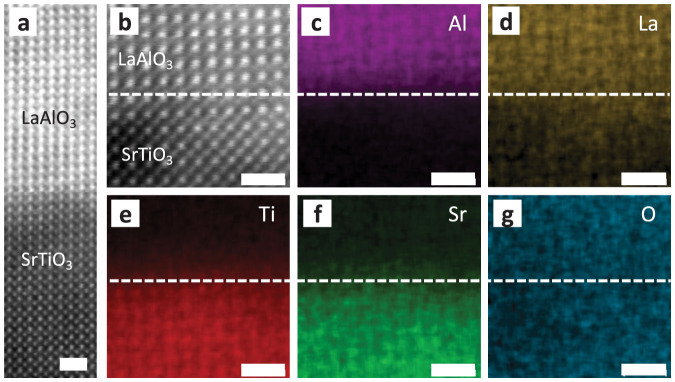
(a) High resolution STEM image of LAO/STO interface. The LAO and STO regions are clearly distinguished from each other in those regions far from interface (>~u.c.). (b) High-magnification STEM image of LAO/STO interface, showing the detailed microstructures close to the interface. (c) to (g) are atomically resolved chemical mapping of Al, La, Ti, Sr, and O respectively, obtained in the same area as (b). Scale bars, 1 nm.
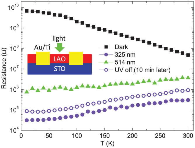
In dark condition, the LAO/STO interface displays insulating behavior as the resistance increases with decreasing temperature, as shown in Figure 2. The insulating behavior of oxide interfaces such as LAO/STO11,21 and NdAlO3/SrTiO323 has been reported previously, which was attributed to disorder induced localization. We observed obvious La intermixing into STO, which is inhomogeneous, as shown in Figure 1d. This inhomogeneity strongly supports that disorder induced localization leads to insulating behavior of our sample. Although there may be doping effects from La, which usually act as donors in STO, the existence of edge dislocations in the vicinity of LAO/STO interface (as shown in Fig. S1) may serve as acceptors, which in some extent keep the interface insulating. Such insulating property provides an opportunity for optoelectronic devices, because it makes it easier to realize large on/off ratio under light illumination. To quantify the on/off ratio, we measured the photoconductivity property at different temperatures, using 325 nm and 514 nm lasers for excitation, respectively. The schematic of our device for photoconductivity measurement is shown in the inset of Figure 2. During measurement, the center area between two electrodes was illuminated and meanwhile we measured current at a constant voltage. Whether light on or off, current-voltage curves were linear. The resistance under 325 nm and 514 nm lasers illumination at different temperatures are plotted in Figure 2. The resistance decreases with decreasing temperature under illumination by 325 nm laser or 514 nm laser, indicating a metallic behavior. Compared to the resistance in dark, the resistance under 325 nm laser illumination falls off by more than two orders of magnitude at 300 K and more than five orders of magnitude at 10 K. The most interesting phenomenon is that the photoconductivity of LAO/STO interface is also notable under 514 nm laser illumination, which changes more than one and nearly four orders of magnitude at 300 K and 10 K, respectively. For comparison, bare STO shows a very large resistance (~1011 Ω) under 514 nm laser illumination (Fig. S2). The resistance of bare STO under illumination of 325 nm laser is also much larger than that of LAO/STO under the same illumination. It can be inferred that the large photoelectric response is originated from the LAO/STO interface. The significant photoelectric response to visible light suggests that there may have midgap states and carrier localizations in the LAO/STO interface.
Figure 2. Temperature dependent resistance of LAO/STO interface.
The samples show an insulating behavior in the dark, while changes to a metallic state under illumination and even light off 10 minutes later. Inset shows the schematic of device structure for photoconductivity measurement.
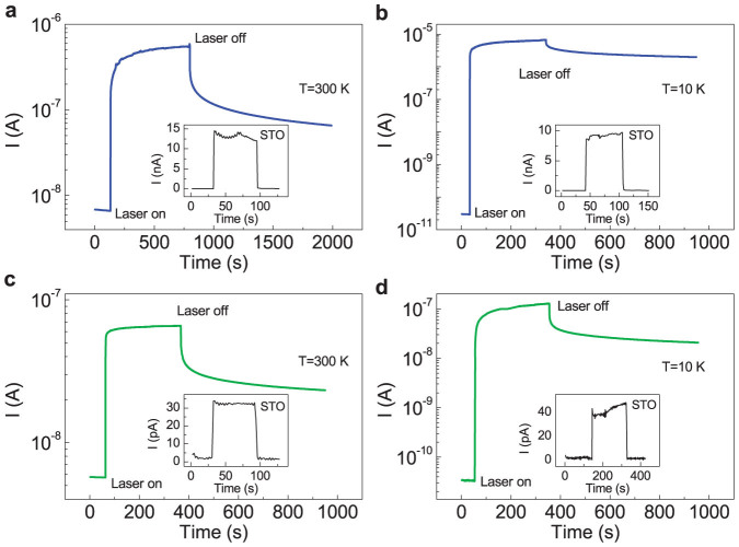
To study the detailed photoconductivity behavior, we measured the temporal dependent photocurrent at a constant voltage. The photoresponse of LAO/STO under illumination of 325 nm laser at room temperature is shown in Figure 3a. Besides a large conductance change from 35 nS to 2.8 μS, a giant persistent photoconductivity after light off was observed. For comparison, photoresponse of bare STO (with the same electrode geometry as LAO/STO) with the same illumination condition is shown in the inset of Figure 3a, which demonstrates a much smaller photoconductivity (only 13 nS) and a fast decay. Although the STEM results show that the STO near the interface may be doped with La, there are not literatures showing PPC in La doped STO. Therefore, we believe that the PPC is not due to the STO. The large PPC of LAO/STO can be attributed to the existence of potential well in LAO/STO interface. Compared to sharp LAO/STO interface, our sample may have a buckled polar interface, and the polar strength may be weakened. Although the chemical abruptness is reduced in our sample, the polar discontinuity may still exist, resulting in the potential well in the interface24. The potential well can trap photo-generated electrons from the localized states, and the trapped electrons need overcome an energy barrier to recombine with holes after light off, resulting in the large PPC. As decreasing temperature from 300 K to 10 K, the photoconductivity increased one order of magnitude and the photocurrent recovery after light off became much slower, as shown in Figure 3b. The improved photoconductivity and enhanced PPC effect at low temperatures are attributed to the reduced phonon scattering and thermal activation19,25. By 514 nm laser illumination, a photoconductance of 250 nS and a similar PPC effect were observed at room temperature, as shown in Figure 3c. However bare STO showed very small photoconductance (only 6.4 pS) at the same condition (inset of Fig. 3c). At 10 K, the LAO/STO device shows a larger photoconductance (~625 nS) and also a slower decay after 514 nm laser off (see Fig. 3d).
Figure 3. Photoelectric response of LAO/STO.
(a), (b) Temporal evolution of photocurrent excited by 325 nm laser at 300 K and 10 K, respectively. (c), (d) Photocurrent response with excitation by 514 nm laser at 300 K and 10 K, respectively. Insets are photoresponse of bare STO for comparison. The 325 nm and 514 nm laser powers are 17 μW and 3.7 mW, respectively. The illumination spot size is ~ 10 μm in diameter. Voltage bias is 0.2 V for all LAO/STO measurements, while 1 V and 5 V for bare STO with illumination of 325 nm and 514 nm lasers, respectively.
Figure 4a demonstrates temporal decay curves of the PPC after switching off the illumination of 325 nm laser at different temperatures. Here, the resistance variation (△RPPC) is normalized by the RPPC measured at the immediate time after switching off the illumination. We can see clearly that the decay becomes faster with increasing temperature. Every decay curve can be well fitted by Kohlrausch stretched exponential expression  25. Decay time constant τ at different temperatures are plotted in Figure 4b, from which we can calculate the activation energy ΔU using expression
  25,26. Here kB is Boltzmann constant. At high temperature region (T > 70 K), the recombination of carriers is dominated by thermal activation with an activation energy of 154 meV, which is larger than that of conductive LAO/STO25. At low temperature region (T < 30 K), the decay time constant τ does not vary with temperature, suggesting a tunneling process dominated electron-hole recombination. A mixture of both recombination processes was observed between 30 K and 70 K. It is notable that the decay is extremely slow (see lnτ in Fig. 4b), indicating that the PPC is rather robust in the measureable time range.
Figure 4. Decay behavior of resistance variation after light off.
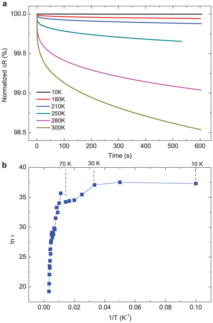
(a) Normalized resistance variation as a function of time after switching off the illumination of 325 nm laser at different temperatures. The decay curves are well fitted by Kohlrausch stretched exponential expression △R ~ exp[-(t/τ)β]. Here τ and β are decay time constant and exponent. (b) ln τ vs the reciprocal of temperature (1/T).
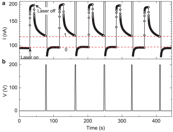
As shown in Figure 2, the R-T curve shows still metallic behavior when 325 nm laser is off ten minutes later. The PPC effect triggers the LAO/STO from high resistance state to low resistance state using light pulse. Applying a back gate voltage, the system can be reset to high resistance state. Figure 5 demonstrates the performance of a prototypical memory based on such oxide interfaces at 300 K. The low resistance state was excited by 514 nm laser. The system maintained at the low resistance state after laser off due to the PPC effect. The PPC was then quenched via applying a back gate voltage pulse of 200 V, realizing a conversion from “1” to “0” state. Employing the metal-insulator transition, the electrically tunable optical switching on/off is more notable than that of the devices based on conductive oxide interfaces19,25,27. At low temperature, the on/off ratio of one order of magnitude was observed (Fig. S3a). Additionally using 325 nm laser as a excitation source is helpful to obtain a lower resistance and the application of 200 V gate voltage pulse leads to a large photocurrent reduction of ΔI ~ 6 μA at 1 V bias (Fig. S3b).
Figure 5. Memory effect of insulating LAO/STO interface.
(a) Revisable memory operation cycles. The 514 nm laser illumination was used for Write operation to produce the On state. The back gate voltage was used for Erase operation to return to the Off state. The source-drain bias voltage of 0.2 V was applied to perform the Read operation. (b) Voltage pulses applied to the back gate. Duration is ~ 2 seconds. The experiments were performed at 300 K.
Discussion
It should be mentioned that the physical mechanism of our memory device is intrinsically different from resistance switching effect in the same system, which relies on oxygen ion transfer28. PPC effect in oxide interfaces is mainly due to carrier being trapped at interfaces. The schematic of the origin of the memory effect illustrating the band structure under photoirradition and gate voltage is shown in Figure 6. When a positive back gate voltage was applied, the potential barrier will be lowered, and electrons trapped at the interface will easily cross the barrier and refill the localized states. The localized electrons will not go back to interface after the back gate voltage is removed, leading to a reduction of carrier density in LAO/STO interface and an increase of resistance as shown in Figure 5. For 325 nm laser excitation, the photogenerated electrons from the bulk STO also can diffuse into the potential well at LAO/STO interface, resulting in a larger PPC and a larger resistance change for the memory devices. At room temperature, thermal activation will result in a reduction of resistance change.
Figure 6. Schematic energy band diagram showing mechanism of memory effect.
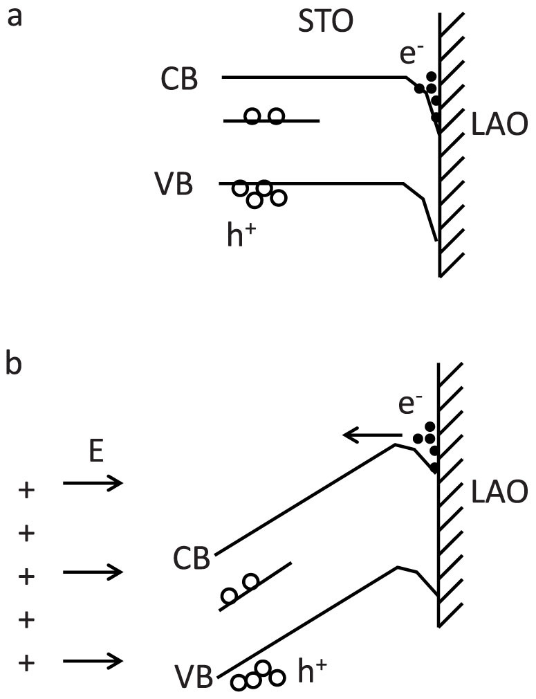
(a) Electrons are trapped in the potential well at the interface after light illumination. (b) The potential barrier is lowered by gate electric field, leading to photocarriers recombination.
In conclusion, we found that the insulating LAO/STO interface can be converted to metallic state by light illumination (UV or visible light). The metallic state still maintains after light is off due to PPC effect. The resistance difference between the PPC and the initial dark state is as large as 104 at 10 K with excitation of 325 nm laser. The decay time constant of PPC in such insulating LAO/STO interface is extremely long, indicating a robust metallic state of PPC. Considering the large decay time constant of PPC and high on/off ratio, we demonstrated a novel application of such insulating LAO/STO interfaces as memory devices, whose “1” state is triggered by light illumination, holds due to PPC effect, and returns to “0” state by application of a back gate voltage. Our results indicate LAO/STO interface is a promising candidate in future information storage devices in oxide electronics.
Methods
Growth
STO (001) substrates with a thickness of 0.5 mm were etched in buffered hydrofluoric acid (BHF) and then annealed in oxygen (0.7 bar) at 1150°C for 1 hour to obtain TiO2 terminated STO. LAO thin film was epitaxially grown on STO by pulsed laser deposition (PLD) using a KrF excimer laser with fluence of ~ 2.1 J/cm2 and a repeat rate of 1 Hz. Substrate temperature was kept at 800°C during deposition with an oxygen pressure of 5 × 10⁻⁴ mbar. After deposition, it was post-annealed in 200 mbar O2 at 600°C for 30 minutes and then cooled down to room temperature at the same pressure.
Characterizations
Cross-sectional samples of LAO/STO were prepared and then the microstructures and atomically resolved element mapping were characterized by spherical aberration corrected scanning transmission electron microscope (Titan G2 80–200 ChemiSTEM, FEI). The interface of LAO/STO was electrically contacted by Ti/Au electrode via the processes including photolithography, Ar ion etching, electron-beam evaporation deposition, and lift-off. Channels with dimensions of 110 μm × 150 μm were defined for investigation. Photoconductivity at temperatures ranging from 10 K to 300 K was measured in a close-cycle helium cryostat, and the excitation by 325 nm and 514 nm laser was guided via a Renishaw inVia confocal optical system. All electrical measurements were performed using Keithley 4200 and Agilent 2912A. 200 V voltage pulses (corresponding to electric field strength of 4 kV/cm) were used to quench the persistent photocurrent. The duration and period of such voltage pulses were 2 S and 80 S respectively.
Author Contributions
Z.M.L. conceived and designed the study. H.L.L. performed the sample growth, device fabrication, and photoelectrical measurements. L.Z. helped to do the experiments. W.T.Y., Y.W., X.M.M. performed the STEM characterizations. D.P.Y. gave scientific advice. H.L.L. and Z.M.L. wrote the manuscript. All authors contributed to discussion and reviewed the manuscript.
Supplementary Material
Supporting Information
Acknowledgments
This work was supported by MOST (Nos. 2013CB934600, 2013CB932602), NSFC (Nos. 11274014, 11234001), the National Fund for Fostering Talents of Basic Science (NFFTBS) with grants No. J1030310, J1103205, and the Program for New Century Excellent Talents in University of China (No. NCET-12-0002).
References
- Ohtomo A. & Hwang H. Y. A High-mobility Electron Gas at the LaAlO3/SrTiO3 Heterointerface. Nature 427, 423–426 (2004). [DOI] [PubMed] [Google Scholar]
- Ben Shalom M., Ron A., Palevski A. & Dagan Y. Shubnikov-De Haas Oscillations in SrTiO3/LaAlO3 Interface. Phys. Rev. Lett. 105, 206401 (2010). [DOI] [PubMed] [Google Scholar]
- Caviglia A. D. et al. Two-Dimensional Quantum Oscillations of the Conductance at LaAlO3/SrTiO3 Interfaces. Phys. Rev. Lett. 105, 236802 (2010). [DOI] [PubMed] [Google Scholar]
- Thiel S., Hammerl G., Schmehl A., Schneider C. W. & Mannhart J. Tunable Quasi-Two-Dimensional Electron Gases in Oxide Heterostructures. Science 313, 1942–1945 (2006). [DOI] [PubMed] [Google Scholar]
- Bell C. et al. Dominant Mobility Modulation by the Electric Field Effect at the LaAlO3/SrTiO3 Interface. Phys. Rev. Lett. 103, 226802 (2009). [DOI] [PubMed] [Google Scholar]
- Brinkman A. et al. Magnetic Effects at the Interface between Non-magnetic Oxides. Nature Mater. 6, 493–496 (2007). [DOI] [PubMed] [Google Scholar]
- Salman Z. et al. Nature of Weak Magnetism in SrTiO3/LaAlO3 Multilayers. Phys. Rev. Lett. 109, 257207 (2012). [DOI] [PubMed] [Google Scholar]
- Kalisky B. et al. Scanning Probe Manipulation of Magnetism at the LaAlO3/SrTiO3 Heterointerface. Nano Lett. 12, 4055–4059 (2012). [DOI] [PubMed] [Google Scholar]
- Reyren N. et al. Superconducting Interfaces between Insulating Oxides. Science 317, 1196–1199 (2007). [DOI] [PubMed] [Google Scholar]
- Biscaras J. et al. Two-dimensional superconductivity at a Mott insulator/band insulator interface LaTiO3/SrTiO3. Nature Communications 1, 1–5 (2010). [DOI] [PubMed] [Google Scholar]
- Caviglia A. D. et al. Electric Field Control of the LaAlO3/SrTiO3 Interface Ground State. Nature 456, 624–627 (2008). [DOI] [PubMed] [Google Scholar]
- Bert J. A. et al. Direct imaging of the coexistence of ferromagnetism and superconductivity at the LaAlO3/SrTiO3 interface. Nat. Phys. 7, 767–771 (2011). [Google Scholar]
- Li L., Richter C., Mannhart J. & Ashoori R. C. Coexistence of magnetic order and two-dimensional superconductivity at LaAlO3/SrTiO3 interfaces. Nat. Phys. 7, 762–766 (2011). [Google Scholar]
- Dikin D. A. et al. Coexistence of Superconductivity and Ferromagnetism in Two Dimensions. Phys. Rev. Lett. 107, 056802 (2011). [DOI] [PubMed] [Google Scholar]
- Ramirez A. P. Oxide Electronics Emerge. Science 315, 1377–1378 (2007). [DOI] [PubMed] [Google Scholar]
- Cen C. et al. Nanoscale Control of An Interfacial Metal-Insulator Transition at Room Temperature. Nature Mater. 7, 298–302 (2008). [DOI] [PubMed] [Google Scholar]
- Cen C., Thiel S., Mannhart J. & Levy J. Oxide Nanoelectronics on Demand. Science 323, 1026–1030 (2009). [DOI] [PubMed] [Google Scholar]
- Irvin P. et al. Rewritable Nanoscale Oxide Photodetector. Nature Photonics 4, 849–852 (2010). [Google Scholar]
- Rastogi A., Kushwaha A. K., Shiyani T., Gangawar A. & Budhani R. C. Electrically Tunable Optical Switching of a Mott Insulator-Band Insulator Interface. Adv. Mater. 22, 4448–4451 (2010). [DOI] [PubMed] [Google Scholar]
- Tebano A., Fabbri E., Pergolesi D., Balestrino G. & Traversa E. Room-Temperature Giant Persistent Photoconductivity in SrTiO3/LaAlO3 Heterostructures. Acs Nano 6, 1278–1283 (2012). [DOI] [PubMed] [Google Scholar]
- Hernandez T., Bark C. W., Felker D. A., Eom C. B. & Rzchowski M. S. Localization of two-dimensional electron gas in LaAlO3/SrTiO3 heterostructures. Phys. Rev. B 85, 161407(R) (2012). [Google Scholar]
- Nakagawa N., Hwang H. Y. & Muller D. A. Why some interfaces cannot be sharp. Nature Mater. 5, 204–209 (2006). [Google Scholar]
- Annadi A. et al. Evolution of variable range hopping in strongly localized two dimensional electron gas at NdAlO3/SrTiO3 (100) heterointerfaces. Appl. Phys. Lett. 101, 231604 (2012). [Google Scholar]
- Yamamoto R. et al. Structural Comparison of n-Type and p-Type LaAlO3/SrTiO3 Interfaces. Phys. Rev. Lett. 107, 036104 (2011). [DOI] [PubMed] [Google Scholar]
- Rastogi A., Pulikkotil J. J., Auluck S., Hossain Z. & Budhani R. C. Photoconducting State and Its Perturbation by Electrostatic Fields in Oxide-based Two-dimensional Electron Gas. Phys. Rev. B 86, 075127 (2012). [Google Scholar]
- Lin J. Y., Dissanayake A., Brown G. & Jiang H. X. Relaxation of Persistent Photoconductivity in Al0.3Ga0.7As. Phys. Rev. B 42, 5855–5858 (1990). [DOI] [PubMed] [Google Scholar]
- Rastogi A. & Budhani R. C. Solar Blind Photoconductivity in Three-terminal Devices of LaAlO3/SrTiO3 Heterostructures. Opt. Lett. 37, 317–319 (2012). [DOI] [PubMed] [Google Scholar]
- Chen Y. Z., Zhao J. L., Sun J. R., Pryds N. & Shen B. G. Resistance Switching at the Interface of LaAlO3/SrTiO3. Appl. Phys. Lett. 97, 123102 (2010). [Google Scholar]
Associated Data
This section collects any data citations, data availability statements, or supplementary materials included in this article.
Supplementary Materials
Supporting Information


