Abstract
This paper introduces a CMOS-microfluidics integration scheme for electrochemical microsystems. A CMOS chip was embedded into a micro-machined silicon carrier. By leveling the CMOS chip and carrier surface to within 100 nm, an expanded obstacle-free surface suitable for photolithography was achieved. Thin film metal planar interconnects were microfabricated to bridge CMOS pads to the perimeter of the carrier, leaving a flat and smooth surface for integrating microfluidic structures. A model device containing SU-8 microfluidic mixers and detection channels crossing over microelectrodes on a CMOS integrated circuit was constructed using the chip-carrier assembly scheme. Functional integrity of microfluidic structures and on-CMOS electrodes was verified by a simultaneous sample dilution and electrochemical detection experiment within multi-channel microfluidics. This lab-on-CMOS integration process is capable of high packing density, is suitable for wafer-level batch production, and opens new opportunities to combine the performance benefits of on-CMOS sensors with lab-on-chip platforms.
1. Introduction
Over the past two decades, many CMOS integrated circuit (IC) based monolithic microsystems have been introduced for analyzing chemical or biological samples. These microsystems have employed optical1-3, electrochemical4, 5, electrical6-8 and magnetic9-11 sensors or actuators. Electrochemical microsystems for example, are capable of populating over one thousand sensors on a CMOS die12. In many applications, sensors need to be physically interfaced with fluid samples, particularly biosensors. Thus, there is an emerging opportunity to combine the capabilities of lab-on-chip sample handling structures with smart sensor microsystems. Integrating these two powerful technologies opens significant opportunities in applications such as high throughput screening, point-of-care diagnosis and implantable devices. However, realizing the full power of such devices is currently hindered by the distinct lack of methods for integrating high density multiple channel microfluidics and CMOS electronics.
Within the field of fluid-environment monolithic sensors, electrochemical microsystems are particularly challenging because they require direct contact between sample fluids and electrodes on ICs13. One major challenge is the topographical conflict between electrical interconnects and microfluidic channels. Wire bonding and solder bumps are reliable electrical interconnection techniques utilized by industry-standard packages such as the dual in-line package (DIP) and the flip-chip chip scale package (FCCSP). Using such standard packages, CMOS ICs have been exposed to liquid samples by adding sealants around bare interconnections to create fluidic reservoirs13, 14. To progress from simple reservoirs toward higher functionality microfluidic channels, flip-chip and solder bumps techniques have been employed without standard packages14. By placing bonding pads to only two opposite sides of a CMOS chip, the real estate conflict between electrical interconnects and fluidic channels was mitigated, permitting a microfluidic channel to run perpendicular to bonding wires at the cost of interconnect density9, 10, 15. Generally, these existing approaches suffer from low yield and cannot be readily adapted to batch fabrication. Moreover, no methods suitable for integrating multiple microfluidic channels with CMOS have been reported.
A major integration challenge derives from the disparity in size between a CMOS chip and microfluidic structures. CMOS chips typically occupy a few square millimeters while microfluidic structures, such as channels, valves, and pumps, require significantly more area and possibly a different set of fabrication processes. To overcome the size disparity issue, CMOS chips have been attached to a substrate carrier that expands the surface area for attachment of a microfluidic channel9, 10. Expanding on this concept, planar electrical interconnects to the carrier have been microfabricated, permitting separation of electrical signal and fluidic circuits onto different planes16-18. However, reducing lateral and vertical displacement between chip and carrier remains a difficult challenge.
To utilize a substrate carrier for leakage-free integration of CMOS electrochemical sensors and high density microfluidics, placement registration error, CMOS-to-carrier surface continuity, CMOS-to-microfluidic bonding and world-to-chip fluidic connection challenges must be resolved. To address these issues, we previously introduced a silicon substrate carrier approach referred to as lab-on-CMOS17. This paper presents an improved lab-on-CMOS process, significantly expands design discussion, and reports test results for a fully integrated microsystem. The new process achieves the best lateral and vertical chip displacements reported to date. SU-8 microfluidics with a taper joint for world-to-chip interconnection is also introduced. On-CMOS electrochemical sensor experiments performed in multiple microfluidic channels are reported.
2. Integration Methods
2.1 Die carrier preparation
To match the real estate needs of microfluidic structures, a silicon substrate carrier, referred to here as a “die carrier”, was adopted to the expand surface area beyond a CMOS chip. AZ 4620 photoresist was spun on a 3 inch diameter and 275 μm thick silicon wafer and patterned with a photomask containing 21 individual 12.5 mm by 12.5 mm die carriers. The rectangular cavities within each carrier were designed to be 10 μm wider than the CMOS chips, allowing some placement freedom while ensuring that the maximum deviation between the centers of the chip and the cavity, i.e., the lateral displacement, was within 5 μm. Deep reactive ion etching (DRIE, Bosch process) was then used to open through-wafer cavities in each carrier on the silicon wafer. After DRIE, 1 μm thermal oxide was grown on the silicon carrier wafer to provide electrical insulation. Dicing streets were patterned and etched at the same time with the cavities. Then, the carriers were singulated along the dicing streets. Alternatively, all carriers could be combined with CMOS chips at the wafer scale and singulated as a final step.
2.2 Chip-carrier leveling and gap filling
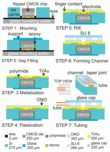
The lab-on-CMOS approach calls for both electrical interconnects and fluidic channels to expand beyond the CMOS chip and onto the die carrier. Because both of these features must across the gap between the carrier and the CMOS chip, vertical displacement between the surfaces of the CMOS chip and the carrier can be catastrophic. Minimizing vertical displacement is essential to successful photolithography-based processing and ultimately to good electrical and fluidic continuity. A chip-to-carrier vertical displacement of 6 μm has been reported by placing a CMOS chip within an etched cavity, where vertical displacement was controlled by the depth of the etched cavity and a precise dose of epoxy16. In contrast, our lab-on-CMOS approach uses a through-wafer cavity and a leveling process designed to minimize vertical displacement. Fig. 1 illustrates the lab-on-CMOS integration process flow for an individual chip-carrier assembly. As shown in step 1, the die carrier is mounted with its polished side down onto a wax-coated (Apiezon wax, M&I Materials, Manchester, UK) glass handling wafer. A CMOS chip is then placed, with its active surface down, into the cavity and gently pressed onto the wax. The chip-carrier assembly is then placed in a 150 °C oven under −20 in.Hg vacuum to reflow the wax and expel trapped air bubbles. The wax reflow process provides self-correction of vertical displacement between the chip and the carrier surfaces. It also attaches the chip and the carrier to the handling wafer and seals the CMOS chip surface to prevent subsequently applied gap-filling materials from seeping under the chip and lifting it up. After cooling, the assembly is visually inspected through the glass handling wafer to confirm that the chip and the carrier are attached to the wax and that no bubbles are present.
Fig.1.
Lab-on-CMOS integration process flow.
Following the chip-carrier leveling process, a gap exists between the CMOS chip and the die carrier. Filling this gap could potentially both bond the parts together and create a solid bridge between their surfaces. To achieve these objectives, an ideal filling material should: (1) have low shrinkage, (2) have low viscosity, (3) not mix with Apiezon wax at room temperature, (4) cure at under 100 °C with low out-gassing or weight loss, (5) be removable by plasma dry etching for surface cleaning, and (6) be resistant to xylene and chlorobenzene (used to remove wax). EPO-TEK 302-3M epoxy (Epoxy Technology, Billerica, MA) was selected because it exhibits these properties. As shown in step 2 of Fig. 1, the epoxy is applied to fill the gap between the chip and carrier. A thin glass support is then attached to the top of the chip-carrier assembly using the gap filling epoxy. This support provides a vacuum seal and additional mechanical strength for subsequent handling. The chip-carrier assembly is then released from the glass handling wafer by softening the wax at 100 °C, and wax residue is cleaned using xylene followed by a rinsing sequence of chlorobenzene, isopropyl alcohol and deionized water. To remove any epoxy that may have reached the chip-carrier surface through imperfect wax sealing, oxygen plasma is applied briefly.
Following these processes, ideally the epoxy is perfectly level with the chip and carrier surfaces. However, in practice the epoxy leaves a shallow trench within the gap it fills. Experiments have shown that the thickness of the wax coating has a major impact on the depth of this trench. If the wax layer is too thick, wax will seep into the gap during reflow, blocking the epoxy and creating a deeper trench. If the wax is too thin, it may not seal well to the chip and carrier and may allow epoxy to seep onto the surfaces. Through experiments, the optimal thickness of wax was identified as 2 μm, which can be obtained from a 1:8 wax dilution in xylene and spin coating at 1000 rpm17.
2.3 Metallization and passivation
To route the CMOS chip pads to the finger contacts at the edges of the die carrier, planar interconnects that cross the chip-carrier trench need to be formed. However, even with a shallow trench, the slope into the trench could be sharp, and the CMOS chip could have exposed silicon along the trench edge. To smooth the trench slopes and any other sharp edges and to insulate any exposed silicon on the chip, a 1:1 dilution of PI-2556 polyimide is applied and patterned by photolithography, as shown in step 3 of Fig. 1. To form planar electrical interconnects, a Ti/Au (5 nm/300 nm) thin film is then deposited by thermal vapor deposition and patterned using liftoff. Ti/Au was chosen because the working electrode (WE) and the counter electrode (CE) of the on-CMOS electrochemical sensors use Au, and this allows both features to be formed from the same layer, at the same time.
Following metallization, a passivation layer is applied to insulate the interconnects and to seal the assembly from undesired exposure to liquids within the microfluidic channels of the final lab-on-CMOS device. As illustrated in step 4 of Fig. 1, a 100 nm oxide/100 nm nitride/100 nm oxide (ONO) passivation layer is deposited at low temperature (100 °C) using an Oxford 80 plasma enhanced chemical vapor deposition (PECVD) system. At 100 °C, the polyimide and the epoxy within the lab-on-CMOS assembly remain stable. The ONO layer is then etched using a LAM 9400 RIE to expose the sensor electrodes on the CMOS chip and the contact fingers at the carrier periphery without exposing the Ti/Au metal film edges, as illustrated in step 5 of Fig. 1. At this point, the CMOS chip surface is protected by its inherent overglass layer plus the added ONO layer. Additionally, all CMOS bonding pads are sealed by Au metallization and the ONO layer.
2.4 Microfluidic-CMOS integration
The final step in the lab-on-CMOS integration process is incorporation of a microfluidic structure onto the chip-carrier assembly. The microfluidic structure is composed of open microfluidic channels covered by a glass cap, as shown in step 6 of Fig. 1. The channels are prepared by spin-coating SU-8 2150 on individual chip-carrier assemblies at 3000 rpm, followed by soft baking, exposure, post exposure baking and development, resulting in a 260 μm layer. The SU-8 is pressed with a glass slide immediately after the soft baking to flatten the top surface. The assembly is then descumed by oxygen plasma (March Instruments PX-250 plasma cleaning system) to remove all SU-8 residues from the gold electrodes. The oxygen plasma also converts the SU-8 surface from hydrophobic to hydrophilic to introduce capillary force. A thin glue layer of SU-8 is then applied to the top surface of the SU-8 open channels by gently pressing the assembly onto a wafer with a 2 μm spin-coated layer of SU-8 2002. A 250 μm thick, 8 mm × 10 mm pre-cut glass cap is then attached to seal the SU-8 open channels.. After the glass cap is attached, the final device, illustrated in step 7 of Fig. 1, is then baked at 95 °C for 2 hrs. This process provides a measured adhesion strength of 25 MPa between the patterned SU-8 layer and the glass cap. Although the prototype lab-on-CMOS device reported here incorporates traditional SU-8 microfluidic structures, many different methods can be adapted to form, for example, complex 3D architectures19 or high pressure channels20.
To enable high density world-to-chip microfluidic interconnections, a method for inserting tubing laterally into the sidewall edge of the SU-8 layer was developed. As shown in step 7 of Fig. 1, inlets and outlets are routed to so-called “taper joints” with a wide tubing guide section that then tapers down to the width of functional channels. The tubing guide is sized to match the diameter of selected tubing that will be held within this section. During insertion, the tapered section helps to clamp the tubing and shield the fluidic channels from potential clogging by epoxy that is applied externally to seal inlet/outlet joints. For the device reported here, a 260 μm tubing guide section was formed to fit TSP100245 flexible fused silica tubing (Polymicro Technologies, Phoenix, AZ, USA) with 100 μm inner diameter and 245 μm outer diameter. This dimension matched the height of the microfluidic structures, which was determined by the SU-8 spin coating rate. The width and height can be adjusted to fit a variety of tubing. To complete the system, two inlet tubes were connected to syringe pumps and an outlet tube was connected to a waste tank.
3. Results and discussion
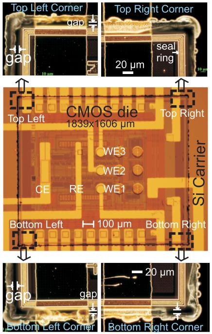
Several silicon die carriers were prepared with a cavity matching the size of a previously reported CMOS potentiostat chip21. Following the assembly steps in Section 2, the CMOS potentiostat chip was placed in a cavity, leveled, fixed and metalized. The lateral displacement between chip and carrier was examined under a microscope. Fig. 2 shows a CMOS chip fixed to a carrier and dark field close-ups of the four corners. The width of gaps between the chip edge and the inner wall of the carrier were measured under a microscope in transmitted light mode by illuminating from the back of the chip through the transparent epoxy trench filler, polyimide and the glass support. The gap measured less than 10 μm along the left edge, and no discernible gap was observed along the right edge, giving maximum x-axis displacement of about 5 μm between the chip and the center of the carrier. The top and the bottom gaps were almost equal, giving nearly zero y-axis displacement. The measurements agreed with the 10 μm freedom allowed for placement. Fig. 2 also shows three working electrodes (WE1, WE2 and WE3), a common reference electrode (RE) and a common counter electrode (CE). All electrodes were electrically connected to the CMOS potentiostat via overglass openings on the chip’s surface and were also routed, through planar interconnects, to the finger contacts at the edge of the carrier for testing.
Fig. 2.
Photograph of the fixed CMOS chip in the silicon die carrier after metallization and magnified dark field images of its four corners.
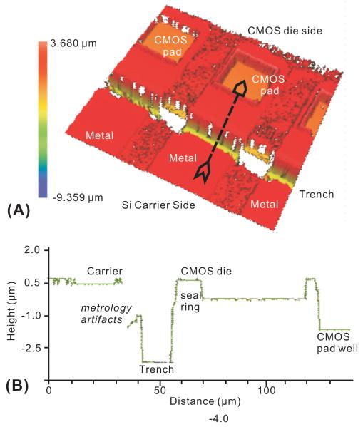
To examine vertical displacement between the CMOS chip and the die carrier, surface profilometry was performed. A normal surface contact profiler uses a stylus that cannot reach down into the bottom of the trench. Instead, 3D profile images of the joint areas were acquired using a Zygo NewView 5000 3D surface profiler with white light interferometry. Fig. 3 shows the 3D surface profile of a chip-carrier joint area and a linear scan across the trench. The linear scan shows that the carrier is vertically aligned within 0.1 μm to the highest feature on the CMOS chip. This is significantly less than the previously reported vertical displacement of 0.5 μm18. Because the sample was required to be tilted for white light interferometry, a portion of the side wall and the bottom of the trench on the carrier side were shadowed, and the linear scan is discontinuous across these regions. The epoxy and polyimide in the trench are also displayed as white because they are transparent and do not reflect light. Thus, the profile was recorded after metallization (step 3 of Fig. 1) in order to observe the bottom of the trench without being affected by metrology artifacts. The trench depth was measured to be about 4 μm. If a PDMS stamp were used for microfluidics, this trench could be a source of leakage that would require application of a polyimide, spin-on glass or other dielectric layer to reduce the trench step. Instead, using SU-8 for microfluidics overcomes potential trench leakage without additional planarization steps. Furthermore, the trench depth will not significantly affect flow because it is very shallow compared to the overall microfluidic channel height (~260 μm). If laminar flow in a shallow microfluidic channel were desired, a planarization step could be included.
Fig. 3.
Surface profile over the chip-carrier joint area. (A) 3D image of the CMOS chip and die carrier separated by a trench; (B) linear scan profile at location of arrow in (A) with x-axis scale roughly 10× the y-axis scale to highlight vertical features.
The quality of metallization across the trench was studied using microscopy, profilometry and resistometry. Observation under an optical microscope showed the metal traces over the trench to be smooth and continuous. The linear scan profile in Fig. 3(B) shows the trench edges to be smooth and the trench slope to be shallow; the slope only appears steep in the image because of different x- and y-axis scaling. To verify the continuity of metal traces, resistance across the trench was measured using a probe station equipped with tungsten probes with 4 μm diameter tips. For a chip-carrier assembly with 5 nm Ti/100 nm Au traces, the resistance from CMOS pads to carrier edge finger contacts was 8.4±0.4 Ω (n=5). The low variation shows consistency and reliability of the interconnects across the trench. This trace resistance is adequately small for all low-to-moderate current applications, including electrochemical sensor measurements.
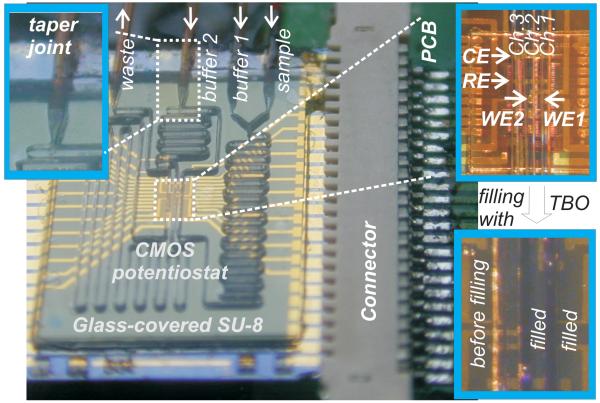
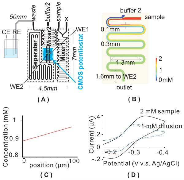
After characterization, the chip-carrier assembly was integrated with a multiple-channel SU-8/glass microfluidic structure to from the complete lab-on-CMOS demonstration device shown in Fig. 4. As shown schematically in Fig. 5(A), the microfluidic structure contains two mixers and a separator, each followed by a detection channel that is routed over the on-CMOS electrodes shown in Fig. 2. Fig. 5(A) also illustrates the fluidic circuit geometries and the electrochemical test setup. The center-to-center distance between adjacent channels is 200 μm. The integrity of the channels was tested by filling the channels with 2mM Toluidine Blue O (TBO) (Sigma-Aldrich, St. Louis, MO, U.S.A.) solution. The right two insets in Fig. 4 show the channels before and during filling with the dark blue TBO solution. No blue color fluid leakage was detected after filling. This demonstration device illustrates the capability of the lab-on-CMOS platform to support complex microfluidics including high density detection channels.
Fig. 4.
The lab-on-CMOS device and schematic of the microfluidic circuits. Insets show (upper left) the taper joint, (upper right) the three microfluidic detection channel across the CMOS potentiostat with on-chip electrodes and (lower right) the microfluidic channels being filled by TBO.
Fig. 5.
Simultaneous dilution and electrochemical detection. (A)Fluidic circuits of the test setup; (B) Simulation of the mixing effect in mixer 2; (C) Mixture concentration profile across the channel width at the outlet of mixer 2; (D) Cyclic voltammogram of the TBO sample on WE2 before and after and its dilution.
The fluidic mixer performance was evaluated to ensure sufficient mixing at designed flow rates. The concentration profile of the 2 mM TBO sample being diluted with buffer in mixer 2 was simulated through a finite element analysis using COMSOL. As Fig. 5(B) shows, the sample and buffer homogenize after 4 turns. The concentration profile at the outlet is plotted in Fig. 5(C) and indicates that the concentration of the diluted TBO is about 0.93±0.04 mM at the outlet. The mixing index, i.e., the standard deviation of normalized concentration, was calculated to be 0.027 at the outlet, suggesting thorough mixing was achieved.
To verify simultaneous fluidic and electrical operation of the Fig. 4 lab-on-CMOS demo device, an experiment involving concurrent sample dilution and electrochemical detection was performed using mixer 2. A sample solution containing 2 mM TBO and 100 mM KCl supporting electrolyte was pumped in via the sample inlet at 0.01 mL/min. The buffer 1 inlet was sealed to disable mixing in mixer 1. The TBO sample ran across WE1 and was then mixed in mixer 2 with a 100 mM KCl solution from the buffer 2 inlet at 0.01 mL/min. The diluted sample then ran across WE2 and was purged through the waste outlet into a tank after flowing through the separator channel. The on-CMOS WE2 embedded in the microfluidic detection channel following the outlet of the mixer 2 was used to electrochemically verify that the sample was diluted through the mixer in situ. A commercial Ag/AgCl RE was placed in the downstream waste tank to provide a reliable reference potential for comparing experimental results with reported values. The on-chip gold quasi RE inherently has a variable potential, and planar Ag/AgCl quasi REs are still in active research22. To ensure that the RE was in the path of current flow between the WEs and CE, an external platinum CE was placed with the external RE. Although the embedded CMOS potentiostat has been shown to successfully perform amperometry experiments21, to further minimize experimental variation, electrochemical measurements were performed by a commercial CHI760 potentiostat (CH Instrument, Austin, TX, USA). The cyclic voltammogram in Fig. 5 (D) shows the current responses of the 2 mM TBO sample at WE2 before and after dilution. As expected, the peak current reduced significantly after dilution. The E1/2 of the dilution measured −268 mV, which compares well with the −245 mV reported in literautre23. This result suggests the electrode surfaces were not contaminated through the lab-on-CMOS microfabrication processes. The E1/2 of the sample before dilution measured −282 mV, indicating that the peak potential shifted as the current increased due to the product of uncompensated solution resistance and higher current. A similar cyclic voltammogram was observed on WE1 by multiplexing the electrodes to the potentiostat. These electrochemical results verify functional operation of the fluidic mixer and the on-CMOS microelectrodes, thus demonstrating the integration capability of the lab-on-CMOS approach. These results represent the first known on-CMOS electrochemical measurements within integrated multichannel microfluidics.
The lab-on-CMOS integration process can readily be adapted to wafer level processing for batch fabrication. Without separating the die carriers from the wafer at the beginning of the process, multiple CMOS chips can be nested into the cavities, leveled and fixed at the same time, and supported on the back by a whole glass wafer. Metallization over CMOS contacts can be kept to within small registration errors from chip to chip. Wafer level processing of lab-on-CMOS not only increases productivity but also grants access to a wide range of advanced planarization and bonding tools, allowing further improvement of interconnects and microfluidics. Moreover, the reported lab-on-CMOS is suitable for the integration of heterogeneous technologies, such as bioMEMS, GaAs and passive or active microfluidic devices, within a single package.
4. Conclusion
A lab-on-CMOS platform that integrates microfluidics, electrode arrays, and CMOS ICs for electrochemical microsystems was introduced. This lab-on-CMOS approach solves the topographical conflict between electrical interconnects and microfluidic channels and allows integration of CMOS instrumentation with a variety of microfluidic structures. The microfabricated planar interconnects and a unique fluidic taper joint overcome challenges of interfacing the device to the real world. Successful use of microfluidic structures and on-CMOS electrodes were demonstrated by electrochemical measurements with a prototype lab-on-CMOS device. The post-CMOS compatible fabrication processes allow high density on-CMOS microfluidics and can be scaled up to wafer-level batch production.
Acknowledgement
The authors would like to thank the National Science Foundation (DBI-0649847) and the National Institutes of Health (RC2ES018756) for funding support and the Lurie Nanofabrication Facility (LNF) and staff at The University of Michigan for fabrication assistance.
References
- 1.Singh RR, Leng L, Guenther A, Genov R. presented in part at the SPIE; San Diego, United States. August 4, 2009. [Google Scholar]
- 2.Hosseini Y, Hartley LF, Kaler KVI. presented in part at the 1st Microsystems and Nanoelectronics Research Conference (MNRC); Ottawa, Canada. October 15, 2008. [Google Scholar]
- 3.Lehmann U, Sergio M, Pietrocola S, Dupont E, Niclass C, Gijs MAM, Charbon E. Sensors and Actuators B: Chemical. 2008;132:411–417. [Google Scholar]
- 4.Frey A, Schienle M, Paulus C, Jun Z, Hofmann F, Schindler-Bauer P, Holzapfl B, Atzesberger M, Beer G, Fritz M, Haneder T, Hanke HC, Thewes R. presented in part at the IEEE International Symposium on Circuits and Systems (ISCAS); Kobe, Japan. May 23-26 2005. [Google Scholar]
- 5.Manickam A, Chevalier A, McDermott M, Ellington AD, Hassibi A. Biomedical Circuits and Systems, IEEE Transactions on. 2010;4:379–390. doi: 10.1109/TBCAS.2010.2081669. [DOI] [PubMed] [Google Scholar]
- 6.Ghafar-Zadeh E, Sawan M, Therriault D. Sensors and Actuators A: Physical. 2008;141:454–462. [Google Scholar]
- 7.Sawan M, Miled MA, Ghafar-Zadeh E. presented in part at the 32nd Annual International Conference of the IEEE Engineering in Medicine and Biology Society (EMBC); Buenos Aires, Argentina. Auguest 31-September 4, 2010. [Google Scholar]
- 8.Manaresi N, Romani A, Medoro G, Altomare L, Leonardi A, Tartagni M, Guerrieri R. Solid-State Circuits, IEEE Journal of. 2003;38:2297–2305. [Google Scholar]
- 9.Lee H, Liu Y, Westervelt RM, Ham D. Solid-State Circuits, IEEE Journal of. 2006;41:1471–1480. [Google Scholar]
- 10.Lee H, Liu Y, Ham D, Westervelt RM. Lab on a Chip. 2007;7:331–337. doi: 10.1039/b700373k. [DOI] [PubMed] [Google Scholar]
- 11.Hua W, Yan C, Hassibi A, Scherer A, Hajimiri A. presented in part at the IEEE International Solid-State Circuits Conference (ISSCC); San Francisco, United States. February 8-12, 2009. [Google Scholar]
- 12.Hwang S, LaFratta CN, Agarwal V, Yu X, Walt DR, Sonkusale S. IEEE Sensors Journal. 2009;9:609–615. [Google Scholar]
- 13.Joo S, Brown RB. Chemical Reviews. 2008;108:638–651. doi: 10.1021/cr068113+. [DOI] [PubMed] [Google Scholar]
- 14.Welch D, Christen JB. Journal of Micromechanics and Microengineering. 2013;23:035009. [Google Scholar]
- 15.Ghafar-Zadeh E, Sawan M, Therriault D, Rajagopalan S, Chodavarapu VP. Microelectronic Engineering. 2009;86:2104–2109. [Google Scholar]
- 16.Li W, Rodger DC, Tai YC. presented in part at the IEEE 21st International Conference on Micro Electro Mechanical Systems (MEMS); Tucson, United States. January 13-17, 2008. [Google Scholar]
- 17.Huang Y, Mason AJ. presented in part at the The 6th Annual IEEE International Conference on Nano/Micro Engineered Molecular Systems (IEEE-NEMS); Kaohsiung, Taiwan. February 20-23, 2011. [Google Scholar]
- 18.Uddin A, Milaninia K, Chin-Hsuan C, Theogarajan L. Components, Packaging and Manufacturing Technology, IEEE Transactions on. 2011;1:1996–2004. doi: 10.1109/TCPMT.2011.2166395. [DOI] [PMC free article] [PubMed] [Google Scholar]
- 19.Agirregabiria M, Blanco FJ, Berganzo J, Arroyo MT, Fullaondo A, Mayora K, Ruano-Lopez JM. Lab on a Chip. 2005;5:545–552. doi: 10.1039/b500519a. [DOI] [PubMed] [Google Scholar]
- 20.Ciftlik AT, Gijs MAM. Lab on a Chip. 2012 doi: 10.1039/c1lc20727j. [DOI] [PubMed] [Google Scholar]
- 21.Huang Y, Mason AJ. presented in part at the IEEE Biomedical Circuits and Systems Conference (BioCAS); Beijing. November 26-28, 2009. [Google Scholar]
- 22.Shinwari W, Zhitomirsky D, Deen I, Selvaganapathy PR, Deen J, Landheer D. Sensors. 2010;10:1679–1715. doi: 10.3390/s100301679. [DOI] [PMC free article] [PubMed] [Google Scholar]
- 23.Schlereth DD, Katz E, Schmidt H-L. Electroanalysis. 1994;6:725–734. [Google Scholar]


