Abstract
Peel-and-stick process, or water-assisted transfer printing (WTP), represents an emerging process for transferring fully fabricated thin-film electronic devices with high yield and fidelity from a SiO2/Si wafer to various non-Si based substrates, including papers, plastics and polymers. This study illustrates that the fundamental working principle of the peel-and-stick process is based on the water-assisted subcritical debonding, for which water reduces the critical adhesion energy of metal-SiO2 interface by 70 ~ 80%, leading to clean and high quality transfer of thin-film electronic devices. Water-assisted subcritical debonding is applicable for a range of metal-SiO2 interfaces, enabling the peel-and-stick process as a general and tunable method for fabricating flexible/transparent thin-film electronic devices.
Fabrication of flexible/transparent thin-film electronic devices on non-Si based substrates faces the critical mismatch challenge between device fabrication conditions and the tolerable conditions for non-Si based substrates in terms of maximum temperature and chemical compatibility1,2,3. Such a challenge is mitigated by transfer printing methods that pick up semiconducting micro/nanomaterials processed on a donor substrate and place them onto a receiver substrate in a massive parallel and deterministic manner3,4,5. Transfer printing methods have enabled the fabrication of flexible/transparent electronic devices, ranging from bio-integrated conformal sensors6,7, curvilinear optoelectronics8 to transient electronics9. Recent advances in transfer printing methods are reviewed thoroughly in ref (3). A key requirement for successful transfer printing process is to weaken the adhesion of the transferred materials to the donor substrate for their easy and defect-free separation3. Such adhesion weakening is commonly achieved by chemical etching, which either creates undercuts underneath the transferred materials to reduce the overall contact surface area or dissolves a sacrificial layer to lift-off the transferred materials from the donor substrates7,8,10.
Recently, we demonstrated a new approach to control the adhesion between the transferred materials and the donor substrates by using room temperature water. The method is named as the peel-and-stick process, or water-assisted transfer printing (WTP) and it is capable of transferring fully fabricated electronic devices from a donor substrate onto an arbitrary receiver substrate. The peel-and-stick process involves three steps (Fig. S1): 1) Fabricating thin-film electronic devices on a metal film (e.g., Ni, Cu) coated SiO2/Si wafer, 2) Peeling-off the metal film together with the top electronic devices from the SiO2/Si wafer in water, and 3) Sticking the peeled electronic devices onto an arbitrary receiver substrate by using commercial adhesive agents. With the peel-and-stick process, we and other groups have successfully transferred a range of electronic devices, including nanowire electronic devices11, amorphous Si thin-film solar cells12, memory devices13 and magnetic nano-devices14, to diverse receiver substrates such as papers, glasses, rubbers, fabrics, plastics and even ultrathin polymer sheets (<1 μm thick). All of these studies demonstrated that the peel-and-stick process can transfer functional thin-film electronic devices with almost a 100% yield regardless of the feature size, thickness and shape without degrading the device performance.
Broader applications of the peel-and-stick process requires the understanding of its fundamental mechanisms in order to achieve customized, controllable and reproducible results for scalable manufacturing of diverse flexible/transparent thin-film electronic devices. In this study, we investigate the fundamental mechanism of the peel-and-stick process by measuring critical adhesion energies of various metal-SiO2 interfaces in air and in water. The results show that the presence of water greatly reduces the critical adhesion energies of the metal-SiO2 interface, leading to facile debonding of the metal film from SiO2/Si wafer in water. The effect of water on the critical adhesion energies of the metal-SiO2 interfaces is further confirmed by our molecular dynamics (MD) simulations using the ReaxFF reactive force field15.
Results
We believe that the easy and clean debonding behavior of the metal-SiO2 interface in water used in the peel-and-stick process is closely related to the environment-assisted subcritical debonding16,17,18,19,20,21. The environment-assisted subcritical debonding refers to interfacial fracture that occurs at the debond driving energy (G) well below the critical adhesion energy (Gc), and it results from stress accelerated chemical reactions between environmental species (e.g., H2O molecules) and strained bonds (e.g., Si-O-Si) at the crack-tip16. The subcritical debonding behavior has been observed for a wide range of materials such as glasses17,18, ceramics22 and polymers23 for several decades and it is usually undesirable and responsible for the failure of a range of thin-film structures. Instead, the peel-and-stick process takes advantage of the environment-assisted subcritical debonding to cleanly peel-off a Ni film, together with the thin-film electronic devices fabricated on top, from the donor Si wafer.
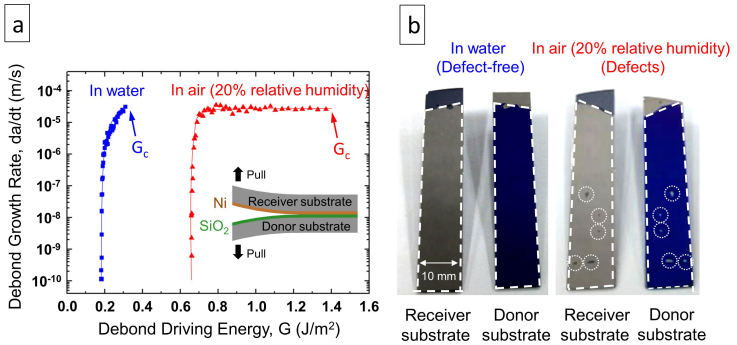
In order to verify that the working principle of the peel-and-stick process is indeed based on the environment-assisted subcritical debonding, we measure the debond growth rates of the Ni-SiO2 interface in air and in water by the standard double-cantilever-beam test24, which is equipped with a high-precision micromechanical test system (Fig. S2a). The double-cantilever-beam test specimen contains a 300 nm thick Ni film that is deposited by an electron beam evaporation on a Si wafer (~525 μm thick) with a thermally grown SiO2 layer (300 nm), and the exposed Ni surface is capped with another Si wafer using an epoxy (Fig. S2b). In Fig. 1, the measured debond growth rate (da/dt) is plotted as a function of the applied debond driving energy (G) for the Ni-SiO2 interface in air with a 20% relative humidity (red dotted line) and in water (blue dotted line) at 21°C. The end point of the da/dt curve corresponds to the interface fracture point and the corresponding driving energy is the critical adhesion energy (Gc). The Gc value of Ni-SiO2 is about 0.31 J/m2 in water, which is around 80% lower than that in air (~1.37 J/m2), confirming that water indeed significantly reduces the required mechanical peel-off forces for separating Ni film from SiO2 surface in the peel-and-stick process. As a comparison, the critical adhesion energy of the as-grown monolayer of graphene-Cu interface is around 0.72 ± 0.07 J/m2 24 for which the interfacial bonding is through the relative weak van der Waals forces. Therefore, the extremely low critical adhesion energy of the Ni-SiO2 interface in water is the main reason for the easy and clean debonding of Ni film together with thin-film electronic devices from the SiO2 surface in the peel-and-stick process. As shown in Fig. 1b, the SiO2 surface is clean and defect-free after the peel-off process of the Ni film in water, but it is covered by visible Ni residue spots after peeling off the Ni film in air owing to the higher mechanical stress.
Figure 1. Debond growth behaviors of the Ni-SiO2 interface.
(a) Debond growth rate (da/dt) as a function of the debond driving energy (G) for the Ni-SiO2 interface in water (blue squares) and in air with a 20% relative humidity (red triangles) at 21°C. Inset schematic shows the double-cantilever-beam specimen geometry used for the measurements. (b) Optical inspection of defects for the delaminated surfaces after the debond test in water (left) and in air (right).
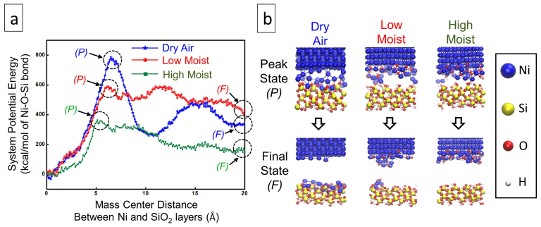
The effect of water on the critical adhesion energy on the Ni-SiO2 interface is further studied by MD simulations using ReaxFF reactive force field15,25,26. The MD simulations investigate the interaction of the Ni film and SiO2 surface under three conditions: dry-air, low-moist and high-moist environments (see the Method section for the MD simulation details). The amount of moisture content is reflected by the initial surface hydroxyl groups (-OH) covered on the Ni surface and hydrogen terminated SiO2 surface. The Ni film and SiO2 surface are initially placed near to each other and then gradually pulled part by increasing their mass center distance in the MD simulations (Supplementary Movies). Figure 2a plots the calculated system potential energy (reference to the initial state) as the mass center distance between the Ni film and SiO2 surface is increased to 20 Å. The system potential energies in all three environments initially increase and then decrease before relaxing to their final states as the mass center distances approach to 20Å, indicating that the system interfaces go through a series of chemical reactions causing by significant rearrangement of the structure. Importantly, the peak system potential energy values, which are related to the critical adhesion energy, decrease in the order of dry-air (600 ~ 800 kcal/mol of Ni-O-Si bond, blue dotted line), low-moist environment (500 ~ 600 kcal/mol of Ni-O-Si bond, red dotted line), and high-moist environment (300 ~ 400 kcal/mol of Ni-O-Si bond, green dotted line). The greatly lowered potential energy barrier with moisture supports our double-cantilever-beam tests (Fig. 1) in that water significantly reduces the critical adhesion energy of Ni-SiO2 interface. Finally, the snapshot images during the MD simulations (Fig. 2b) clearly show that high moisture leads to less interfacial bonding at the peak potential energy state (P) and less Ni residues on SiO2 surface at the final state (F), agreeing well with the experimental observations in Fig. 1b.
Figure 2. Molecular Dynamics (MD) simulations of the peel-off process.
(a) Comparison of the system potential energy as increasing the mass center distance between Ni layer and SiO2 layer in dry-air (blue dotted line), low-moist (red dotted line) and high-moist (green dotted line) environments. (b) Snapshots corresponding to the peak state (P) and final state (F) in the three different environments, respectively.
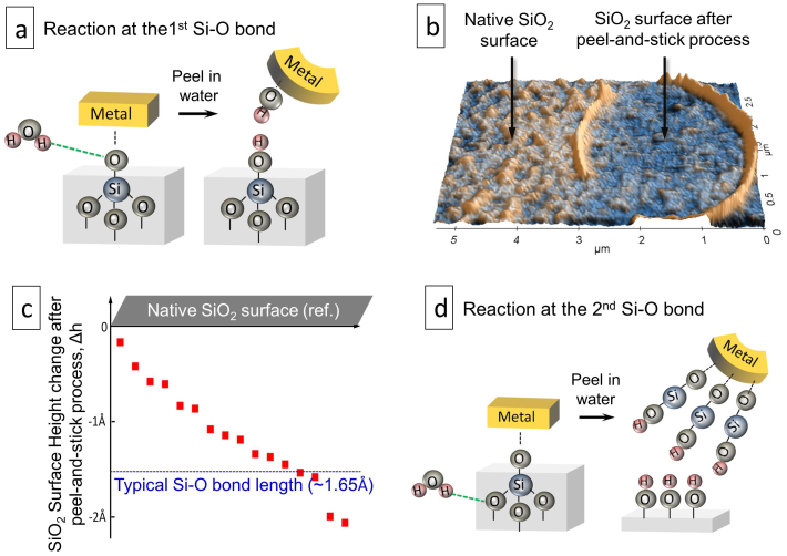
Both double-cantilever-beam tests and MD simulations indicate that the peel-and-stick process is controlled by the environment-, or more precisely water-, assisted subcritical debonding that is caused by accelerated chemical reactions between the highly strained surface bonds at the crack-tip (e.g., Si-O-Si) and the environmental species (e.g., H2O molecules)16,17. Previous studies of the water-assisted subcritical debonding phenomenon on the bulk glass (SiO2/SiO2 interface) suggested that water has a strong polar interaction with the strained Si-O-Si crack-tip bonds, leading to the rupture of the hydrogen bond in water and the formation of surface Si-O-H groups on both sides of the fractured surfaces17,19. In the peel-and-stick process, the Ni-O-Si bond is believed to form during the deposition of Ni film. During the peel-off process in water, the applied mechanical peel-off stress deforms the Ni-O-Si crack-tip bond that readily reacts with H2O molecules to form Ni-O-H and Si-O-H on each side of the fractured surface (Fig. 3a). To verify this, we compare the surface topography of two SiO2 surfaces with/without going through the Ni peel-off process in water. The left side of the atomic force microscopy (AFM) image in Fig. 3b corresponds to the topography of the native SiO2 surface without going through the peel-and-stick process, and the right circled area in Fig. 3b matches with the transformed SiO2 surface after a sequential deposition and peel-off in water of a circular Ni disk (300 nm thick and 3 μm in diameter). It is clear that the right circled SiO2 surface is smoother than the native SiO2 surface, indicating that the surface is modified by the peel-and-stick process. It should be noted that the circular wall in Fig. 3b corresponds to the Ni residue at edges of the Ni disk after the peel-and-stick process and is used to locate the modified SiO2 surface during the AFM measurements. Figure 3c plots the differences of the average surface height (Δh) between the native SiO2 surface (left in Fig. 3b) and the modified SiO2 surface (right in Fig. 3b) within a defined area (0.7 μm × 0.7 μm) for 16 different samples. The average surface height differences range from nearly 0 Å to about −2.1 Å with an average of −1.2 ± 0.5 Å. The nearly zero height difference corresponds to the mechanism described in Fig. 3a, (i.e.,  ). Given that the Si-O bond length is about 1.65 Å (blue dotted line in Fig. 3c), the larger height difference in the two SiO2 surfaces indicates that water can also access and react with the strained Si-O-Si bond located at the 2nd atomic layer from the top surface of SiO2 (Fig. 3d). Such interaction is especially prominent for the surface area with convexed topography, leading to the smoothing of the SiO2 surface on the right side (Fig. 3b). In both cases (Fig. 3a and 3d), the delaminated surfaces are terminated with hydroxyl (-OH) groups and are hydrophilic, which facilitates the further adsorption of H2O molecules and continuous reactions along the Ni-SiO2 interface.
Figure 3. Associated molecular reaction mechanisms for the peel-and-stick process.
(a) Reaction between a water molecule and a strained Si-O bond at crack-tip. (b) An atomic force microscopy (AFM) image for corresponding SiO2 surfaces without (left side) or with (right side) going through the peel-and-stick process. (c) Average height differences (Δh) between the left side and right side of the SiO2 surface in Fig. 3b. (d) Reaction between a water molecule and a strained Si-O-Si bond located at the 2nd atomic layer from the top SiO2 surface.
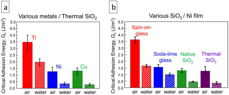
With the understanding of the fundamental working principles, we can improve the generality and controllability of the peel-and-stick process to accommodate different transfer needs. The water-assisted subcritical debonding should occur for different metal-SiO2 interfaces. In Fig. 4a, two other metal films of Ti (red) and Cu (green) are tested respectively as a debonding layer on a thermally grown SiO2 surface in comparison to Ni (blue). The measured critical adhesion energy for the Ti-SiO2 interface in air with a relative humidity of 20%, due to its inherent strong interaction, is about three times higher than those of the Ni-SiO2 or Cu-SiO2 interfaces27. More importantly, for all three cases, the critical adhesion energies in water are about 1/2 to 1/4 of those in air.
Figure 4. Critical adhesion energy (Gc) in air with a 20% relative humidity and in water at 21°C for (a) interface between thermally grown SiO2 and Ti, Ni and Cu, respectively and (b) interface between Ni and various SiO2, including spin-on-glass, soda-lime glass, native SiO2 and thermal SiO2.
In addition to the various metal choices, the peel-and-stick process is equally applicable to different types of SiO2 surfaces. Figure 4b shows the critical adhesion energies in air with a 20% relative humidity and in water at 21°C between a 300 nm thick Ni film and different types of SiO2 surfaces, including spin-on-glass (red), soda-lime glass (blue), native SiO2 (green) and thermally grown SiO2 (purple). The commercial spin-on-glass (Futurrex®, IC1-200) has the highest critical adhesion energy in air (~3.6 J/m2) and in water (~1.5 J/m2) due to its inherent strong adhesive properties. And thus, the delaminated surfaces after the double-cantilever-beam test show clear signs of defects (Fig. S3). The soda-lime glass (Fisher Scientific®) has slightly higher adhesion energy in air, but significantly higher adhesion energy in water in comparison to the native and thermally grown SiO2. The smaller reduction of critical adhesion energy by water for the soda-lime glass is likely because it contains other chemical compositions in addition to SiO2, implying that SiO2 is more susceptible to the water reaction than other chemical compositions. The native SiO2 and thermally grown SiO2 layers have similar low critical adhesion energies both in air and in water, so these two SiO2 surfaces are most suitable for high quality peel-and-stick process. Importantly, regardless of the metal-SiO2 combinations, water clearly reduces the critical adhesion energy (Fig. 4). It should be noted that the critical adhesion energy can be further reduced by varying other environmental factors, such as temperatures, pH values, environmental species, film thicknesses and residual stresses18,19. Therefore, the peel-and-stick process can be implemented with various combinations of metal-SiO2 interfaces and carried out under controlled environmental conditions to accommodate diverse transfer needs for the fabrication of flexible/transparent thin-film electronic devices.
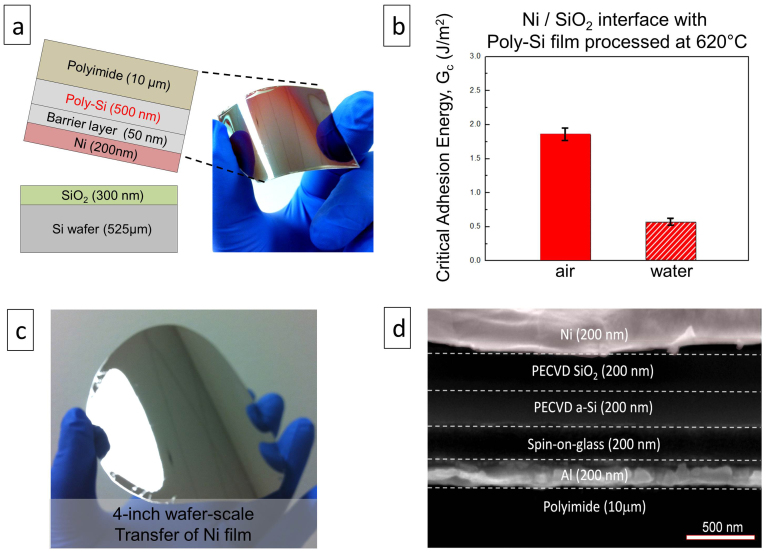
Finally, we demonstrate several important features of the peel-and-stick process to illustrate its potential for manufacturing high-performance thin-film electronic devices on flexible/transparent substrates. First, the peel-and-stick process can transfer materials and devices processed at high temperatures for high-performance electronics, since both SiO2 and metal (i.e., Ni has a melting temperature of 1455°C) can sustain relatively high temperatures. To illustrate this, a thin poly-silicon (poly-Si) film is coated on a Ni-coated SiO2/Si wafer by the solid phase recrystallization of amorphous Si at 620°C, and a flexible polyimide (10 μm) with maximum allowable temperature of around 350°C is subsequently spin-coated on top of the poly-Si film as a receiver substrate (Fig. 5a, schematic). Next, the Ni film is peeled off manually from the SiO2 surface in water and chemically etched away for optical inspection. The optical image in Fig. 5a shows that the delaminated poly-Si film appears clean and defect-free. The critical adhesion energy of this particular Ni-SiO2 interface structure is also significantly lowered by water (Fig. 5b), and its adhesion energy in water is 0.56 ± 0.04 J/m2 which is slightly higher than the bare Ni-SiO2 interface (0.35 ± 0.11 J/m2 as shown in Fig. 4a). This difference results from the high temperature annealing process of poly-Si film that induces additional residual stress on the Ni film, increasing the critical adhesion energy28. Nonetheless, the reduced critical adhesion energy in water is still low enough for successful peel-and-stick process. Furthermore, the peel-and-stick process is scalable for transferring large area thin-film electronic devices because the water-assisted subcritical debonding is independent of the surface area. For example, a 4-inch wafer-scale Ni film is cleanly peeled off from a SiO2/Si wafer with the peel-and-stick process (Fig. 5c). It should be noted that the scalability of the peel-and-stick process ultimately depends on the mechanical properties of the transferred materials/devices since the possibility of mechanical failure increases with increasing area. Such mechanical issues can be alleviated by 1) designing the device structures to improve the overall device flexibility29,30 or 2) minimizing the device layer deformation during the water peel-off process with a rigid temporary holder. The last important feature of the peel-and-stick process is that it can transfer a stack of thin-films of different materials that are commonly used for electronic devices. For example, thin-film transistors are consisted of different layers of gate metal contacts, dielectrics oxides, semiconductors and source/drain metal contacts. Figure 5d shows a SEM image of 6-layer-stacked thin-films that are successfully transferred together from a SiO2/Si wafer to a flexible plastic substrate. Note that the delaminated Ni layer is shown on the very top. The multiple layers used here consist of representative materials for general electronic devices, such as metals (Ni, Al), semiconductor (amorphous-Si), insulating oxides (SiO2) and polymer (polyimide), and they are deposited by a range of techniques including electron-beam evaporation, plasma-enhanced chemical vapor deposition (PECVD) and spin-coating. Importantly, there is no sign of any crack between the multiple layers because the Ni-SiO2 interface has the lowest interfacial adhesion energy in water. These results show that the peel-and-stick process has the merits of high-temperature compatibility, scalability and multiple-layer-transfer capability.
Figure 5. Important features of the peel-and-stick process.
(a) A schematic (left) of the peel-and-stick process to transfer the poly-Si film processed at 620°C onto a flexible polyimide substrate directly deposited on top. An optical image (right) of the clean and defect-free surface of the poly-Si film after the peel-and-stick process. (b) Critical adhesion energy (Gc) of Ni-SiO2 interface in air with a 20% relative humidity and in water at 21°C for the particular case of transferring the poly-Si film. (c) An optical image of a 4-inch wafer-scale transferred Ni film from a SiO2/Si wafer onto a flexible plastic substrate. (d) A SEM image of the transferred 6-layer-stacked thin-films from a SiO2/Si wafer to a flexible plastic substrate.
Discussion
The present study reveals that the fundamental working principle of the peel-and-stick process is based on the water-assisted subcritical debonding between metal-SiO2 interfaces. Both the double-cantilever-beam tests and MD simulations clearly show that water significantly reduces the critical adhesion energy of the metal-SiO2 interface, which leads to the clean and defect-free transfer of electronic devices from a donor Si substrate to any receiver substrate. In addition, the water-assisted subcritical debonding is observed for a range of metal-SiO2 interfaces and the critical adhesion energy can be further tuned by varying different environment conditions. As such, we believe that the peel-and-stick process can be tailored and applied for the scalable manufacturing of diverse flexible/transparent thin-film electronics, ranging from organic light emitting diodes, inorganic thin film transistors, to many emerging hybrid high-performance thin-film electronic devices.
Methods
Molecular dynamics (MD) modeling
Three models are prepared for MD simulations corresponding to the dry-air, low-moist and high-moist environments, respectively. The Ni layer has a total of 216 Ni atoms with its (111) surface. The SiO2 layer is a 2-D expansion from a cristobalite unit cell structure containing 128 atoms with one surface layer consisting of under coordinated oxygen atoms and another surface layer of hydroxyl (-OH) terminated Si atoms. The two layers are initially placed near each other with a mass center distance of 11 Å. This value is chosen so that the two layers can generate a proper initial contact. In low- and high-moist environments, the Ni layer is covered with surface hydroxyl groups; the first layer of under coordinated oxygen atoms in the SiO2 layer is terminated with hydrogen atoms. The two layers are placed in a similar fashion as that in dry-air environment. The difference between low- and high-moist environments lies in the surface coverage ( ) of hydroxyl groups (0.5 and 0.75 for low- and high-moist environment, respectively). All the systems are equilibrated for 2.5 ps in the isothermal-isobaric ensemble at 300 K allowing for free volume adjustment. The mass center distance of the two layers is then increased to 20 Å in 5 ps in the canonical ensemble. The temperature is controlled at 300K using the Berendsen thermostat with a damping constant of 100 fs. The MD time step is 0.25 fs.
Author Contributions
C.H.L. and X.L.Z. designed the experiments and simulations. J.H.K. and T.S.K. conducted double-cantilever-beam tests for measuring critical adhesion energies. C.Z. and A.C.T.D. performed molecular dynamics simulations. Q.W. and N.W. deposited the poly-silicon film. C.H.L., I.S.C., J.M.W., X.L.Z. conducted the atomic force microscopy analysis and characterization of the peel-and-stick process. C.H.L. and X.L.Z. prepared the manuscript, and all authors discussed the results and commented on the manuscript.
Supplementary Material
Supplementary Information
Video S1
Video S2
Video S3
Acknowledgments
X.L.Z. acknowledges the financial support by the Samsung Global Research Outreach Program (SPO#: 107915). T.S.K. acknowledges financial support from the National Research Foundation of Korea (NRF-2012R1A1A1006072). NREL work is supported by the U.S. Department of Energy under contract DE-AC36-08-GO28308. ACTvD and CZ acknowledge funding from the National Energy Technology Laboratory-Regional University Association (NETL/RUA). RES Activity Number 600.220.001 AETRI.
References
- Kim M.-G., Kanatzidis M. G., Facchetti A. & Marks T. J. Low-temperature fabrication of high-performance metal oxide thin-film electronics via combustion processing. Nat. Mater. 10, 382–388 (2011). [DOI] [PubMed] [Google Scholar]
- Lee C. H., Kim D. R. & Zheng X. L. Fabricating nanowire devices on diverse substrates by simple transfer-printing methods. Proc. Nati. Acad. Sci. USA. 107, 9950–9955 (2010). [DOI] [PMC free article] [PubMed] [Google Scholar]
- Carlson A., Bowen A. M., Huang Y., Nuzzo R. G. & Rogers J. A. Transfer Printing Techniques for Materials Assembly and Micro/Nanodevice Fabrication. Adv. Mater. 24, 5284–5318 (2012). [DOI] [PubMed] [Google Scholar]
- Kim S. et al. Microstructured elastomeric surfaces with reversible adhesion and examples of their use in deterministic assembly by transfer printing. Proc. Nati. Acad. Sci. USA. 107, 17095–17100 (2010). [DOI] [PMC free article] [PubMed] [Google Scholar]
- Meitl M. A. et al. Transfer printing by kinetic control of adhesion to an elastomeric stamp. Nat. Mater. 5, 33–38 (2006). [Google Scholar]
- Viventi J. et al. Flexible, foldable, actively multiplexed, high-density electrode array for mapping brain activity in vivo. Nat. Neurosci. 14, 1599–1605 (2011). [DOI] [PMC free article] [PubMed] [Google Scholar]
- Kim D.-H. et al. Dissolvable films of silk fibroin for ultrathin conformal bio-integrated electronics. Nat. Mater. 9, 511–517 (2010). [DOI] [PMC free article] [PubMed] [Google Scholar]
- Yoon J. S. et al. GaAs photovoltaics and optoelectronics using releasable multilayer epitaxial assemblies. Nature 465, 126–131 (2010). [DOI] [PubMed] [Google Scholar]
- Hwang S.-W. et al. A Physically Transient Form of Silicon Electronics. Science 337, 1640–1644 (2012). [DOI] [PMC free article] [PubMed] [Google Scholar]
- Yang Y. et al. Arrays of Silicon Micro/Nanostructures Formed in Suspended Configurations for Deterministic Assembly Using Flat and Roller-Type Stamps. Small 7, 484–491 (2011). [DOI] [PubMed] [Google Scholar]
- Lee C. H., Kim D. R. & Zheng X. Fabrication of Nanowire Electronics on Nonconventional Substrates by Water-Assisted Transfer Printing Method. Nano Lett. 11, 3435–3439 (2011). [DOI] [PubMed] [Google Scholar]
- Lee C. H. et al. Peel-and-Stick: Fabricating Thin Film Solar Cell on Universal Substrates. Sci. Rep. 2, 1000 (2012). [DOI] [PMC free article] [PubMed] [Google Scholar]
- Choi J. M., Kim M. S., Seol M. L. & Choi Y. K. Transfer of functional memory devices to any substrate. Phys. Status Solidi RRL 5, 326–331 (2013). [Google Scholar]
- Donolato M., Tollan C., Maria Porro J., Berger A. & Vavassori P. Flexible and Stretchable Polymers with Embedded Magnetic Nanostructures. Adv. Mater. 25, 623–629 (2012). [DOI] [PubMed] [Google Scholar]
- Van Duin A. C. T., Dasgupta S., Lorant F. & Goddard W. A. ReaxFF: A reactive force field for hydrocarbons. J. Phys. Chem. A 105, 9396–9409 (2001). [Google Scholar]
- Birringer R. P., Shaviv R., Besser P. R. & Dauskardt R. H. Environmentally assisted debonding of copper/barrier interfaces. Acta Mater. 60, 2219–2228 (2012). [Google Scholar]
- Wiederhorn S. M. Influence of Water Vapor on Crack Propagation in Glass. Am. Ceram. Soc. Bull. 50, 407–414 (1967). [Google Scholar]
- Card J. C., Cannon R. M., Saiz E., Tomsia A. P. & Ritchie R. O. On the physics of moisture-induced cracking in metal-glass (copper-silica) interfaces. J. Appl. Phys. 102, 053516 (2007). [Google Scholar]
- Guyer E. P. & Dauskardt R. H. Fracture of nanoporous thin-film glasses. Nat. Mater. 3, 53–57 (2004). [DOI] [PubMed] [Google Scholar]
- Kook S. Y. & Dauskardt R. H. Moisture-assisted subcritical debonding of a polymer/metal interface. J. Appl. Phys. 91, 1293–1303 (2002). [Google Scholar]
- Michalske T. A. & Freiman S. W. A Molecular Interpretation of Stress-Corrosion in Silica. Nature 295, 511–512 (1982). [Google Scholar]
- Wiederhorn S. M. Moisture Assisted Crack Growth in Ceramics. Int. J. Fract. Mech. 4, 171–177 (1968). [Google Scholar]
- Kook S. Y. & Dauskardt R. H. Moisture-assisted subcritical debonding of a polymer/metal interface. J. Appl.Phys. 91, 1293–1303 (2002). [Google Scholar]
- Yoon T. et al. Direct Measurement of Adhesion Energy of Monolayer Graphene As-Grown on Copper and Its Application to Renewable Transfer Process. Nano Lett. 12, 1448–1452 (2012). [DOI] [PubMed] [Google Scholar]
- Mueller J. E., Van Duin A. C. T. & Goddard W. A. III Development and Validation of ReaxFF Reactive Force Field for Hydrocarbon Chemistry Catalyzed by Nickel. J. Phys. Chem. C 114, 4939–4949 (2010). [Google Scholar]
- Fogarty J. C., Aktulga H. M., Grama A. Y., Van Duin A. C. T. & Pandit S. A. A reactive molecular dynamics simulation of the silica-water interface. J. Chem. Phys. 132 (2010). [DOI] [PubMed] [Google Scholar]
- Vitos L., Ruban A. V., Skriver H. L. & Kollar J. The surface energy of metals. Surf. Sci. 411, 186–202 (1998). [Google Scholar]
- Nie P., Shen Y., Chen Q. & Cai X. Effects of residual stresses on interfacial adhesion measurement. Mech. Mater. 41, 545–552 (2009). [Google Scholar]
- Kim D. H. et al. Optimized Structural Designs for Stretchable Silicon Integrated Circuits. Small 5, 2841–2847 (2009). [DOI] [PubMed] [Google Scholar]
- Kim S. et al. Imbricate Scales as a Design Construct for Microsystem Technologies. Small 8, 901–906 (2011). [DOI] [PubMed] [Google Scholar]
Associated Data
This section collects any data citations, data availability statements, or supplementary materials included in this article.
Supplementary Materials
Supplementary Information
Video S1
Video S2
Video S3


