Abstract
The local interplay between the ionic and electronic transport in NiO is explored using correlative imaging by first-order reversal curve measurements in current-voltage and electrochemical strain microscopy. Electronic current and electromechanical response are observed in reversible and electroforming regime. These studies provide insight into local mechanisms of electroresistive phenomena in NiO and establish universal method to study interplay between the ionic and electronic transport and electrochemical transformations in mixed electronic-ionic conductors.
For over a century, electrochemical phenomena in solids were intensively explored in the context of energy storage and conversion devices1,2, electrochromic systems3, corrosion, and metallurgy. Recently, much attention has been attracted to coupling between ionic and electronic transport phenomena, as exemplified by electroresistive materials and devices4. While the early applications of electroresistive systems date back for more than century (e.g. electronic coherer5) and much work on fundamental mechanisms of electroresistance was performed in 1950ies, this field now sees a renaissance both due to emergence of new materials synthesis and nanofabrication technologies and recognized limitations of the complementary metal-oxide semiconductor (CMOS) technologies6,7. The electroresistive systems are now actively explored in the context of non-volatile highly scalable information storage, memristive and neuromorphic electronics7,8,9.
The processes involved in formation and operation of electroresistive oxide memories in oxides are very complex and involve multiple electronic and ionic transport steps and electrochemical transformations, often in nanometer volumes of active devices or conductive filaments and their junctions. As such, they sensitively depend on external stimuli, including bias levels, boundary conditions at the electrodes, initial microstructure, and forming currents, etc.
The general sequence of events in electroforming of a material can be represented as following. For small external biases, only electronic conductivity is observed. For higher biases, the mobile ion subsystem is polarized, leading to accumulation/depletion of ions at electrodes. Associated changes in conductance lead to gradual development of in-plane instabilities that eventually gives rise to nucleation of new phases and formation of conductive filaments7,10,11. In some materials, further bias increase (typically under galvanostatic control) leads to soft breakdown and formation of conductive filament (forming). In others, the reaction front is stable and bulk resistive switching is observed. In both cases, formation of gaseous products and oxygen adsorption on surfaces are observed, suggesting the role of gas-solid reactivity. Much effort has been directed towards controlling the electroresistive phenomena, e.g. through layers with given stoichiometry and device fabrication7,9,10,12,13,14.
The design and optimization of electroresistive devices necessitates understanding of local ionic, electronic, and thermal phenomena over all stages of resistive switching, to determine the role of intrinsic defects and inhomogeneities on these processes. Recently, a number of studies of conductive filament formation in memristors was studied by (scanning) transmission electron and scanning probe microscopies (SPM) at nearly atomic resolution, providing the information on the structure and electronic properties of the formed filament15,16,17,18,19,20. In particular, atomically controlled electrochemical reactions including nucleation and subsequent growth have been recently explored and provided information on the electrochemical kinetics of the conductive filament formation18,19,20,21. More recently, conductive filament formation has been studied on the nanoscale using current atomic force microscopy22. However, there is still lack of information on the electronic and ionic phenomena that precede the formation of conductive filaments, including ionic polarization, possible gas-solid reactions, and nucleation of conductive phase.
Here we report the combined studies of electronic and ionic dynamics in NiO using correlative multimodal SPM. The electrochemical strain microscopy (ESM) demonstrates the presence of strong hysteretic electromechanical response, indicative of bias-induced ionic transport. We further combine the first-order reversal curves (FORC) measurements in electrochemical strain microscopy23,24,25 and in I-V measurements to decouple reversible and irreversible processes. This correlative multimodal FORC IV and ESM imaging allows probing local mechanisms of electroresistive phenomena in NiO and establishing universal methodology to study the interplay between the ionic and electronic transport and electrochemical transformations in mixed electronic-ionic conductors26.
Results
Electrochemical strain microscopy and spectroscopy of NiO
As a model system, we have chosen NiO. In the stoichiometric form, NiO is a classical cubic charge-transfer insulator. The changes in oxygen stoichiometry or doping by e.g. Li readily induce metal-insulator transition. The former can be controlled by electric bias, and consequently NiO is one of the most popular resistive switching materials7,10,11,14,27. Here, a 50 nm polycrystalline NiO1−x thin film was prepared by sputtering method on SrRuO3/SrTiO3 substrate to explore electronic and ionic dynamics using SPM. The details of the sample preparation and electrical properties can be found elsewhere27.
The ionic dynamics in NiO is probed by electrochemical strain microscopy (ESM)23,24,25,28,29. In ESM, application of electric bias to a SPM tip leads to redistribution of mobile ions in the tip field and possible gas-solid reactions. The changes in molar volume and associated electrochemical strains lead to surface deformation that is detected by an SPM tip in the form of high-frequency (0.1–1 MHz) ESM signal. Indeed, strain effects induced by oxygen reactions were observed with atomic resolution using SPM30. In ESM voltage spectroscopy, the response is measured as a function of slowly (~1 Hz) changing triangular voltage waveform, providing information on the bias-induced ionic processes below the tip. These imaging and spectroscopic modes are similar to those adopted in piezoresponse force microscopy (PFM)31,32, with the difference being in the signal generation mechanisms involved in imaging (piezoelectric response vs. bias-induced ionic motion) and spectroscopies (polarization switching vs. electrochemical reactions).
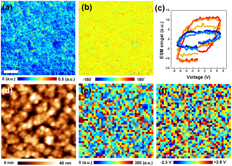
Shown in Figure 1(d) is surface topography of the NiO film, exhibiting a clear grain structure. The ESM line images are shown in Figures 1(a, b), illustrating the presence of ESM response of the pristine film. The locally varied ESM hysteresis loops can be observed as shown in Figure 1(c). The ESM hysteresis loops can be further analyzed over a dense grid of points33 to extract the maps of effective switching parameters, as shown in Figures 1(e, f). The spatial maps of switching parameters in Figures 1(e, f) also show locally different electrochemical performance24.
Figure 1.
ESM (a) amplitude and (b) phase images. (c) Selected ESM hysteresis loops as measured at different locations. (d) Topography and spatial maps of (e) work of switching (area under the loop) and (f) imprint (difference between x-intercepts). Scale bar is 200 nm.
The observation of the strong electromechanical response in NiO and its hysteresis under external bias sweep strongly indicates the presence of ionic phenomena. Indeed, electromechanical response per se can originate from the piezoelectric effect, deformation potential effects, ionic motion and associated Vegard strains, and flexoelectric effect34,35,36, as well as more subtle electromechanical couplings enabled by symmetry breaking at surfaces37. In cubic NiO, the bulk piezoelectric effect (and hence ferroelectricity) can be excluded. The deformation potential and flexoelectric effects describe fast responses of the ionic sub-system to changes in the local electrochemical potential and field gradients respectively, and can contribute to the high-frequency ESM response. However, observation of ESM hysteresis loop is indicative of either thermodynamic bistability (e.g. similar to that in ferroelectrics), or slow ionic or domain dynamics. In NiO, the latter can be attributed to the tip-induced ionic motion. We note that while some of the ionically-induced electromehcnical responses can be non-trivial, e.g. due to the renormalization of the first term or Ginzburg-Landau free energy for polar mode or flexoeffect, the controlling factor is still ionic dynamic36.
Note that observation of cyclostationary ESM hysteresis loops suggest that the bias-induced ionic process is reversible or largely reversible (thus specifically excluding electroforming regions). In the NiO sample studied here, the ESM measurements are possible only in the +/−15 V bias interval. The application of higher biases leads to electroforming and dielectric breakdown, with associated large-scale changes in conductance and surface structure, as explored below.
Probing ionic and electronic dynamics by first-order reversal curve spectroscopies
The ESM studies of NiO provide some insight into the local ionic phenomena in this material, as reflected in the spatial variability of the ESM response and hysteresis loops. However, comprehensive characterization of electroresistance mechanism brings forward two challenges, namely (a) probing of both ionic and electronic degrees of freedom locally and (b) exploring the evolution of these responses during the irreversible processes. Current imaging or ESM imaging under a constant dc or ac condition does not provide any information on the evolution of these responses. Furthermore, a single hysteresis loop IV and ESM imaging can provide only limited information under a specific case. Thus, to address these challenges, we develop an approach based on correlative multimodal probing of ionic and electronic behaviors utilizing FORC method38,39,40,41 applied to ESM and current-voltage (I-V) measurements.
Macroscopic I-V curve measurement is a well-established approach for characterization of electroresistive systems. For low voltages, application of bias to the tip does not alter the chemical state of the system. In this case, the I-V curve is non-hysteretic, i.e. forward and reverse curves coincide. For higher biases, the electronic flow through the system induces (reversible) changes in chemical or physical state of the material, including ionic polarization or local reduction. The relaxation processes are generally slow and are associated with significant kinetic or thermodynamic hysteresis. Correspondingly, the I-V curves become hysteretic in nature. Finally, formation of conductive filaments is associated with sharp changes in conductivity, constituting electroresistive switching.
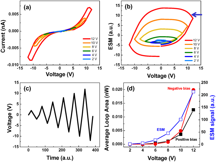
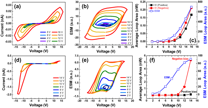
To explore these phenomena systematically, we implement the FORC I-V measurements in SPM spectroscopic imaging mode. Here, current collected from the bottom electrode is measured for the voltage profile shown in Figure 2(c). The area of the I-V hysteresis loop opening is probed as a function of the peak bias. For low biases, the I-V curves are non-hysteretic (or currents are below detection limit), whereas the onset of ionic transport is associated with a hysteresis loop opening (see Fig. 2(a)). Correspondingly, the hysteresis loop opening vs. peak bias provides insight into the bias-induced electrochemical phenomena.
Figure 2. Average FORC type (a) I-V and (b) ESM loops as a function of varying bias (c); (d) corresponding loop area averaged over 1600 spatial points.
Similar approach can be applied in ESM and PFM. For PFM, the FORC method allows local Preisach densities to be identified42,43. For ESM, the FORC provides information on the development of ionic activity as a function of bias and allows separating of reaction and transport processes44.
Several relevant comments regarding these methods should be made. At a single spatial location, FORC ESM and FORC I-V can both be applied to explore reversible and irreversible electrochemical processes. However, imaging on dense spatial grids (i.e. volume affected by bias is larger than pixel spacing) is possible only for reversible (or, more rigorously, cyclostationary) processes, while only sparse grids can be used for irreversible processes and generally spatially resolved imaging is unlikely45. That said, the onset of irreversibility can be readily detected from images (streaks and abrupt changes of contrast, etc.).
The high locality of electric field produced by SPM tip strongly affects the measurement mechanisms. Since bias is local, it suppresses (albeit not obviates) the filamentary instabilities usual in uniform electric fields (e.g. compare to ferroelectric polarization switching in PFM46,47,48,49,50,51). Secondly, the ESM provides information on phenomena adjacent to the tip, i.e. within the signal generation volume that is commensurate with the tip-surface contact area52,53,54. While this processes can be affected by global conductivity of the film55, these effects are secondary and ESM signal can be observed even on purely ionic conductors23. Finally, the ESM signal is generally proportional to the ionic concentration.
In comparison, I-V measurements measure the overall resistance between the tip and bottom electrode. While the spreading resistance of the tip-surface junction provides the dominant contribution to the signal for uniform materials, situation can be different for inhomogeneous systems. Examples include the dislocation mediated conductance in STO where single defect establishes conductive path in the insulating matrix56. Opposite case is a grain boundary system, in which grain boundaries at large separation from the tip-surface junction control resistance measured by SPM57,58,59,60,61,62. The current depends on the local ionic concentration; however, direct interpretation of spreading resistance in terms of carrier concentration is possible only for Ohmic conductance. For realistic materials, the I-V curves are highly non-linear63,64,65, precluding direct quantification in terms of relevant materials properties.
Local ionic and electronic phenomena in NiO: reversible regime
The discussion above illustrates that the information provided by the FORC I-V and FORC ESM methods can be expected to be highly complementary. Here, we combine these two approaches in a correlative multimodal imaging mode, as shown in Figure 2. Figure 2(a) illustrates the evolution of the FORC I-V curves for small biases (in the reversible region). The corresponding ESM FORC data is shown in Figure 2(b). The peak bias dependence of the hysteresis loop area for I-V and ESM data is shown in Figure 2(d).
The I-V curves are strongly non-linear, exhibiting shape characteristic for the mixed electronic-ionic conductors63,64,65. The hysteresis loop opening in the I-V curve can then directly be attributed to the onset of ionic motion below the probe. The characteristic loop shape with regions of negative susceptibility at the turning points (on decreasing the bias hysteresis loop continues to increase) (see blue arrow in Figure 2(b)) strongly indicates the kinetic nature of the observed behavior. Remarkably, qualitatively similar behaviors are observed in the ESM data (Figure 2(d)). Here, for small bias windows the hysteresis loops are essentially closed and have characteristic lozenge shape. On increasing the bias, the loops evolve towards more rectangular shape; however the regions with negative susceptibility are also visible. Notably, the behavior of IV and ESM loop opening vs. bias is also very similar, hinting at the similarity of underpinning mechanism. This behavior is readily understandable in reversible regime, when vacancy accumulation below the tip provide linear correction both to electronic conduction and ESM signal. We also note that ESM loop opening occurs earlier than I-V loop opening. This originates from the fact that ionic motion can be detected by ESM even at lower bias which is not sufficient for current flowing through the films66.
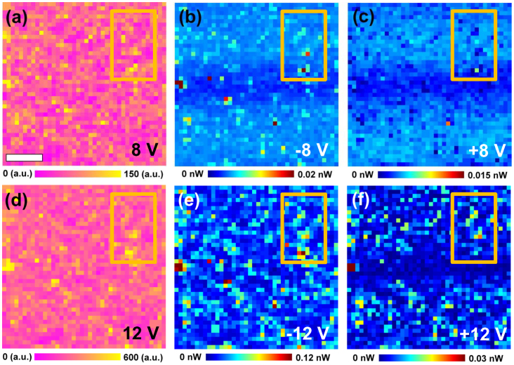
We further explore spatial localization of electrochemical and ionic activity on the NiO surface. In this, measurements such as those in Figure 2 are performed at each point of a dense spatial grid (40 × 40 pixels with 25 nm pixel size). Note that the grid size is such that only several points fall within single grain. However, attempts at imaging with higher pixel densities typically lead to the irreversible surface degradation and were unsuccessful.
Shown in Figures 3(a, d) are the ESM hysteresis loop opening maps for the 8 V and 12 V bias windows (note that FORC data set by definition contains similar images for all bias windows with ideal spatial alignment). The presence of regions of higher- and lower ESM activity with the characteristic size of several tens of nm, i.e. comparable to single grain size is clearly seen. The corresponding images for the FORC I-V measurements are shown in Figures 3(b, c, e, and f). Similarly to the ESM maps, clear localization of hysteresis responses associated with the individual grains is observed.
Figure 3. Spatial maps of (a, d) ESM loop area, (b, e) negative I-V loop area, and (c, f) positive I-V loop area for (a–c) 8 V and (d–f) 12 V, respectively.
Scale bar is 200 nm.
Of immediate interest is correlation between the ESM and I-V hysteretic behavior. In many cases, such correlation can be established based on the qualitative similarity of the images (large scale features, etc.). This is possible for the images in Figure 3; however, small feature size renders such comparison unreliable and it lacks quantitative power. To explore this behavior systematically, we perform cross-correlation analysis of the images. Here, the cross-correlation coefficient for two images is defined as:
 |
where images are represented as matrices A and B of equal size taken over identical spatial grid,  = mean(A) and
  = mean(B).
The cross-correlation between two images acquired at different biases establishes the measure of resemblance between the two, with a correlation coefficient of ‘1' meaning that features in both images are identical, ‘−1' being opposite (so that a minimum in one corresponds to a maximum in the other), and ‘0' meaning that the images are unrelated. Note that this analysis is limited in extracting the underlying relationships between data – for example the cross-correlation between topographic image and its derivative will be close to ‘0' (i.e. lack of correlation does not indicate lack of dependence); more complex multivariate statistical techniques can be used in these cases.
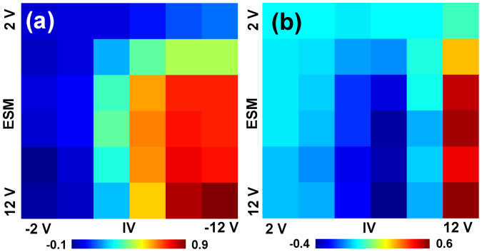
Shown in Figure 4 is the bias-dependent correlation between the ESM and I-V hysteresis signals defined as  , where
  and
and  are the ESM and I-V hysteresis loop opening images at given biases. The correlation was calculated for negative and positive branches of the I-V loops separately. For negative biases, correlation matrix
  is close zero for small biases, as expected for largely noise-dominated images. However, for large biases the correlation values are close to 1. This suggest that regions which has strongly hysteretic behavior in ESM also have strong hysteretic behavior in I-V curves, indicative of the common origin of the signals. For the positive biases, the behavior is remarkably different. Here, in the 6 ~ 8 V interval the
  elements are negative, suggesting that the ESM activity is anti-correlated with the I-V. These features can be observed in the spatial maps of ESM loop area and I-V loop area in the orange boxes of Fig. 3. We note that some regions, i.e. grain boundaries, show opposite contrast dependent on the magnitude of biases. This means that these regions have dissimilar mechanisms of electrochemical response.
Figure 4. Correlation between ESM loop area and I-V loop area spatial maps for (a) negative and (b) positive biases.
Irreversible regime
On increasing the bias window, the material and tip become prone to irreversible changes of conductance (electroforming and tip degradation). The critical biases for these phenomena are position dependent, and in many cases their onset can be detected by spurious changes of ESM and I-V response during spectroscopic image acquisition. Note that once electroforming happened for the first time, the size of the affected area is often larger than the characteristic grid spacing, and hence all remaining measurements are taken on the electroformed region. Here we specifically aim to explore this regime to understand the changes in correlated IV and ESM behavior during electroforming.
This behavior is illustrated in a set of FORC I-V and FORC ESM data in Figure 5 acquired sequentially for bias windows higher then stability region (previous section). For the first 10 points, the system remains in the pristine state, as shown in Figure 5. The hysteresis loop behavior is close to that in Figure 2, except that due to the higher bias the loops are more saturated. Again, the I-V and ESM loop opening exhibit similar dynamics.
Figure 5. Average FORC type (a, d) I-V and (b, e) ESM loops and (c, f) corresponding loop areas for (a–c) 10 points without any changes in surface state and (d–f) subsequent 1600 points including electroforming.
However, on continuous cycling the electroforming process occurs, with drastic changes in both I-V and ESM behavior. The I-V curve becomes strongly rectifying and the maximal current increases by ~2 orders of magnitude. At the same time, the ESM hysteresis loops exhibit strong vertical shift, adopt almost square shape without the negative susceptibility regions, and effective response decreases by ~1 order of magnitude.
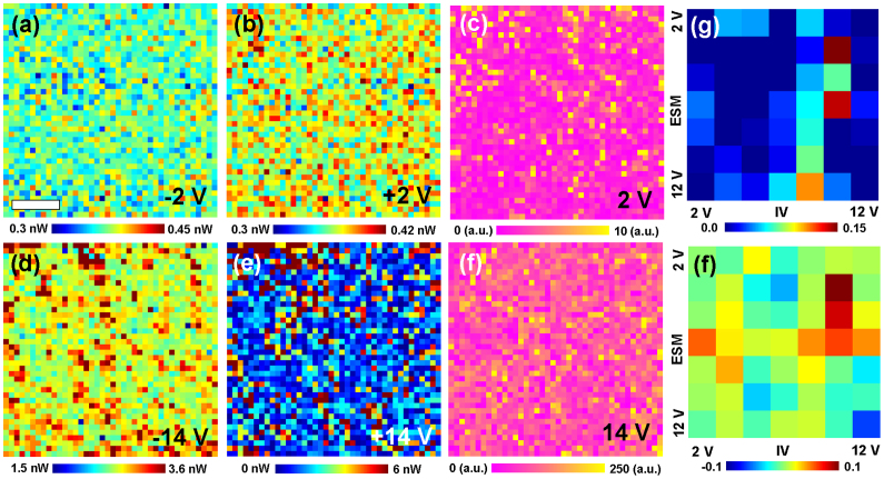
The corresponding hysteresis loop area maps are shown in Figure 6. The clear spatially correlated features are visible in both ESM and I-V loop area maps. However, in this case the correlation between ESM and I-V behavior has almost disappeared. We attribute this behavior to the forming process in NiO. For intermediate biases, the oxygen vacancies accumulate below the tip, giving rise to large ESM responses and pronounced hysteresis in I-V and ESM loops. However, the system remains in the non-conductive state. On further bias increase, the nucleation of metallic phase occurs, with associated increase of electronic conductivity and decrease of ionic mobility.
Figure 6. Spatial maps of (a, d) negative I-V loop area, (b, e) positive I-V loop area, and (c, f) ESM loop area for (a–c) 2 V and (d–f) 14 V, respectively.
Correlation between ESM loop area and I-V loop area for (g) negative and (h) positive biases.
Discussion
We have explored the interplay between electronic and ionic activity during the electroforming in NiO using newly introduced correlative multimodal imaging by FORC measurements in I-V and ESM. While conventional current or ESM imaging can provide only limited information on the electrochemical performance, the correlative multimodal imaging approach can provide electrochemical information of both ionic and electronic degrees of freedom locally. For small biases, both I-V and ESM provide the information on progressive vacancy accumulation under the probe with associated increase of zero-bias resistance and ESM loop opening as well as the contrast formation mechanisms. For large biases, the electroforming process occurs with a drastic increase of electronic conductivity and decrease of ESM responses, indicative of the conductive phase nucleation. These studies can be extended to other systems, most notably ferroelectric, tunneling barriers, fuel cells, etc., which allow local probing based on the electronic and electromechanical phenomena.
Methods
Materials
A 50 nm polycrystalline NiO1−x thin film was prepared by sputtering method on SrRuO3/SrTiO3 substrate (substrate temperature: 500°C, working pressure of Ar + O2 mixture gas: 1.5 mTorr, O2 ratio: 7%) to explore electronic and ionic dynamics using SPM. The surface roughness and grain size are about 8.852 and 122.3 nm, respectively. The details of the sample preparation and electrical properties can be found elsewhere27.
SPM measurements
Ambient SPM studies were performed with a commercial system (Asylum Research Cypher) additionally equipped with a current amplifier (FEMTO DLPCA-200) and LabView/Matlab based software. ESM and I-V measurements were simultaneously carried out with applying biases to Pt/Cr coated tips (the radius of the tip: <25 nm, Budget sensors Multi75E-G). The spatial resolution of the ESM and I-V maps is 25 nm.
Author Contributions
Y.K. and S.V.K. proposed the concept. Y.K. E.S. and S.J. developed the measurement technique and analysis tools. Y.K. performed the experiments. I.H., T.C., B.H.P. prepared the samples. Y.K. and S.V.K. wrote the manuscript. All authors discussed the results and commented on the manuscript.
Acknowledgments
Research was supported (S.V.K., Y.K.) by the U.S. Department of Energy, Basic Energy Sciences, Materials Sciences and Engineering Division. A portion of this research was conducted at the Center for Nanophase Materials Sciences (S.V.K., S.J., E.S.), which is sponsored at Oak Ridge National Laboratory by the Scientific User Facilities Division, Office of Basic Energy Sciences, U.S. Department of Energy. This work was also supported by (I.R.H., B.H.P.) the National Research Foundation of Korea(NRF) grants funded by the Korea government (MSIP) (No. 2013R1A3A2042120) and (T.C.) Basic Science Research Program through the NRF funded by the Korea MEST (Grant No. 2011-0025607).
References
- Bagotsky V. S. Fuel Cells: problems and solutions. (Wiley, 2009). [Google Scholar]
- Kendall, K. & Singhal, S. C. (ed.) High-temperature solid oxide fuel cells: fundamentals, design and applications (Elsevier Science, 2003). [Google Scholar]
- Granqvist C. G. Oxide electrochromics: an introduction to devices and materials. Sol. Energy Mater. Sol. Cells 99, 1–13 (2012). [Google Scholar]
- Szot K. et al. TiO2-a prototypical memristive material. Nanotechnology 22, 254001 (2011). [DOI] [PubMed] [Google Scholar]
- Coherer, http://en.wikipedia.org/wiki/Coherer (2013) Date of acess 03/10/2013. [Google Scholar]
- Strukov D. B., Snider G. S., Stewart D. R. & Williams R. S. The missing memristor found. Nature 453, 80–83 (2008). [DOI] [PubMed] [Google Scholar]
- Sawa A. Resistive switching in transition metal oxides. Mater. Today 11, 28–36 (2008). [Google Scholar]
- Jo S. H. et al. Nanoscale memristor device as synapse in neuromorphic systems. Nano Lett. 10, 1297–1301 (2010). [DOI] [PubMed] [Google Scholar]
- Ha S. D. & Ramanathan S. Adaptive oxide electronics: A review. J. Appl. Phys. 110, 071101 (2011). [Google Scholar]
- Waser R. & Aono M. Nanoionics-based resistive switching memories. Nature Mater. 6, 833–840 (2007). [DOI] [PubMed] [Google Scholar]
- Waser R., Dittmann R., Staikov G. & Szot K. Redox-based resistive switching memories - nanoionic mechanisms, prospects, and challenges. Adv. Mater. 21, 2632 (2009). [DOI] [PubMed] [Google Scholar]
- Yang J. J. et al. Memristive switching mechanism for metal/oxide/metal nanodevices. Nature Nanotechnol. 3, 429–433 (2008). [DOI] [PubMed] [Google Scholar]
- Yang J. J. S., Strukov D. B. & Stewart D. R. Memristive devices for computing. Nature Nanotechnol. 8, 13–24 (2013). [DOI] [PubMed] [Google Scholar]
- Kim K. M., Jeong D. S. & Hwang C. S. Nanofilamentary resistive switching in binary oxide system; a review on the present status and outlook. Nanotechnology 22, 254002 (2011). [DOI] [PubMed] [Google Scholar]
- Kwon D. H. et al. Atomic structure of conducting nanofilaments in TiO2 resistive switching memory. Nature Nanotechnol. 5, 148–153 (2010). [DOI] [PubMed] [Google Scholar]
- Yang Y. C. et al. Observation of conducting filament growth in nanoscale resistive memories. Nature Comm. 3, 1–8 (2012). [DOI] [PubMed] [Google Scholar]
- Tappertzhofen S., Mundelein H., Valov I. & Waser R. Nanoionic transport and electrochemical reactions in resistively switching silicon dioxide. Nanoscale 4, 3040–3043 (2012). [DOI] [PubMed] [Google Scholar]
- Tsuruoka T., Terabe K., Hasegawa T. & Aono M. Temperature effects on the switching kinetics of a Cu-Ta2O5-based atomic switch. Nanotechnology 22, 254013 (2011). [DOI] [PubMed] [Google Scholar]
- Valov I. et al. Atomically controlled electrochemical nucleation at superionic solid electrolyte surfaces. Nature Mater. 11, 530–535 (2012). [DOI] [PubMed] [Google Scholar]
- Valov I. & Staikov G. Nucleation and growth phenomena in nanosized electrochemical systems for resistive switching memories. J. Solid. State Electr. 17, 365–371 (2013). [Google Scholar]
- Terabe K., Hasegawa T., Nakayama T. & Aono M. Quantized conductance atomic switch. Nature 433, 47–50 (2005). [DOI] [PubMed] [Google Scholar]
- Nardi F. et al. Switching of nanosized filaments in NiO by conductive atomic force microscopy. J. Appl. Phys. 112, 064310 (2012). [Google Scholar]
- Kumar A., Ciucci F., Morozovska A. N., Kalinin S. V. & Jesse S. Measuring oxygen reduction/evolution reactions on the nanoscale. Nature Chem. 3, 707–713 (2011). [DOI] [PubMed] [Google Scholar]
- Balke N. et al. Nanoscale mapping of ion diffusion in a lithium-ion battery cathode. Nature Nanotechnol. 5, 749–754 (2010). [DOI] [PubMed] [Google Scholar]
- Balke N. et al. Real space mapping of Li-ion transport in amorphous Si anodes with nanometer resolution. Nano Lett. 10, 3420–3425 (2010). [DOI] [PubMed] [Google Scholar]
- Strelcov E. et al. Probing local ionic dynamics in functional oxides at the nanoscale. Nano Lett. 13, 3455–3462 (2013). [DOI] [PubMed] [Google Scholar]
- Choi J. S. et al. Different resistance switching behaviors of NiO thin films deposited on Pt and SrRuO3 electrodes. Appl. Phys. Lett. 95, 022109 (2009). [Google Scholar]
- Morozovska A. N., Eliseev E. A. & Kalinin S. V. Electromechanical probing of ionic currents in energy storage materials. Appl. Phys. Lett. 96, 222906 (2010). [Google Scholar]
- Jesse S. et al. Direct mapping of ionic transport in a Si anode on the nanoscale: time domain electrochemical strain spectroscopy study. ACS Nano 5, 9682–9695 (2011). [DOI] [PubMed] [Google Scholar]
- Cai Z. H. et al. Surface electronic structure transitions at high temperature on perovskite oxides: the case of strained La0.8Sr0.2CoO3 thin films. J. Am. Chem. Soc. 133, 17696–17704 (2011). [DOI] [PubMed] [Google Scholar]
- Gruverman A. & Kholkin A. Nanoscale ferroelectrics: processing, characterization and future trends. Rep. Prog.Phys. 69, 2443–2474 (2006). [Google Scholar]
- Kalinin S. V., Rar A. & Jesse S. A decade of piezoresponse force microscopy: progress, challenges, and opportunities. IEEE T. Ultrason. Ferr. 53, 2226–2252 (2006). [DOI] [PubMed] [Google Scholar]
- Jesse S., Lee H. N. & Kalinin S. V. Quantitative mapping of switching behavior in piezoresponse force microscopy. Rev. Sci. Instrum. 77, 073702 (2006). [Google Scholar]
- Morozovska A. N. et al. Thermodynamics of electromechanically coupled mixed ionic-electronic conductors: deformation potential, Vegard strains, and flexoelectric effect. Phys. Rev. B 83, 195313 (2011). [Google Scholar]
- Morozovska A. N., Eliseev E. A., Svechnikov G. S. & Kalinin S. V. Nanoscale electromechanics of paraelectric materials with mobile charges: size effects and nonlinearity of electromechanical response of SrTiO3 films. Phys. Rev.B 84, 045402 (2011). [Google Scholar]
- Kim Y. et al. Ionically-mediated electromechanical hysteresis in transition metal oxides. ACS Nano 6, 7026–7033 (2012). [DOI] [PubMed] [Google Scholar]
- Tagantsev A. K. Piezoelectricity and flexoelectricity in crystalline dielectrics. Phys. Rev. B 34, 5883–5889 (1986). [DOI] [PubMed] [Google Scholar]
- Katzgraber H. G., Gary F. B. & Zimanyi G. T. Fingerprinting hysteresis. Physica B 343, 10–14 (2004). [Google Scholar]
- Roberts A. P., Pike C. R. & Verosub K. L. First-order reversal curve diagrams: A new tool for characterizing the magnetic properties of natural samples. J. Geophys. Res.-Solid Earth 105, 28461–28475 (2000). [Google Scholar]
- Mayergoyz I. D. & Friedman G. Generalized Preisach model of hysteresis. IEEE Trans. Magn. 24, 212–217 (1988). [Google Scholar]
- Mayergoyz I. D. Mathematical-models of hysteresis. Phys. Rev. Lett. 56, 1518–1521 (1986). [DOI] [PubMed] [Google Scholar]
- Guo S. et al. Spatially resolved probing of Preisach density in polycrystalline ferroelectric thin films. J. Appl. Phys. 108, 084103 (2010). [Google Scholar]
- Ovchinnikov O. et al. Local measurements of Preisach density in polycrystalline ferroelectric capacitors using piezoresponse force spectroscopy. Appl. Phys. Lett. 96, 112906 (2010). [Google Scholar]
- Balke N. et al. Decoupling electrochemical reaction and diffusion processes in ionically-conductive solids on the nanometer scale. ACS Nano 4, 7349–7357 (2010). [DOI] [PubMed] [Google Scholar]
- Jesse S., Maksymovych P. & Kalinin S. V. Rapid multidimensional data acquisition in scanning probe microscopy applied to local polarization dynamics and voltage dependent contact mechanics. Appl. Phys. Lett. 93, 112903 (2008). [Google Scholar]
- Morozovska A. N. et al. Thermodynamics of nanodomain formation and breakdown in scanning probe microscopy: Landau-Ginzburg-Devonshire approach. Phys. Rev. B 80, 214110 (2009). [Google Scholar]
- Molotskii M. I. & Shvebelman M. M. Dynamics of ferroelectric domain formation in an atomic force microscope. Philos. Mag. 85, 1637–1655 (2005). [Google Scholar]
- Kalinin S. V. et al. Nanoelectromechanics of polarization switching in piezoresponse force microscopy. J. Appl. Phys. 97 (2005). [Google Scholar]
- Kalinin S. V. et al. Intrinsic single-domain switching in ferroelectric materials on a nearly ideal surface. Proc. Natl Acad. Sci.USA 104, 20204–20209 (2007). [DOI] [PMC free article] [PubMed] [Google Scholar]
- Morozovska A. N., Eliseev E. A. & Kalinin S. V. Domain nucleation and hysteresis loop shape in piezoresponse force spectroscopy. Appl. Phys. Lett. 89, 192901 (2006). [Google Scholar]
- Agronin A., Rosenwaks Y. & Rosenman G. Direct observation of pinning centers in ferroelectrics. Appl. Phys. Lett. 88, 072911 (2006). [Google Scholar]
- Morozovska A. N. et al. Frequency dependent dynamical electromechanical response of mixed ionic-electronic conductors. J. Appl. Phys. 111, 014107 (2012). [Google Scholar]
- Morozovska A. N., Eliseev E. A. & Kalinin S. V. Electrochemical strain microscopy with blocking electrodes: The role of electromigration and diffusion. J. Appl. Phys. 111, 014114 (2012). [Google Scholar]
- Morozovska A. N., Eliseev E. A., Balke N. & Kalinin S. V. Local probing of ionic diffusion by electrochemical strain microscopy: Spatial resolution and signal formation mechanisms. J. Appl. Phys. 108, 053712 (2010). [Google Scholar]
- Kalinin S. V., Jesse S., Tselev A., Baddorf A. P. & Balke N. The role of electrochemical phenomena in scanning probe microscopy of ferroelectric thin films. ACS Nano 5, 5683–5691 (2011). [DOI] [PubMed] [Google Scholar]
- Szot K., Speier W., Bihlmayer G. & Waser R. Switching the electrical resistance of individual dislocations in single-crystalline SrTiO3. Nature Mater. 5, 312–320 (2006). [DOI] [PubMed] [Google Scholar]
- Bonnell D. A., Huey B. & Carroll D. In-situ measurement of electric-fields at individual grain-boundaries in TiO2. Solid State Ion. 75, 35–42 (1995). [Google Scholar]
- Huey B. D. & Bonnell D. A. Spatially localized dynamic properties of individual interfaces in semiconducting oxides. Appl. Phys. Lett. 76, 1012–1014 (2000). [Google Scholar]
- Shao R., Kalinin S. V. & Bonnell D. A. Local impedance imaging and spectroscopy of polycrystalline ZnO using contact atomic force microscopy. Appl. Phys. Lett. 82, 1869–1871 (2003). [Google Scholar]
- Kalinin S. V. & Bonnell D. A. Local electronic transport at grain boundaries in Nb-doped SrTiO3. Phys. Rev. B 70, 235304 (2004). [Google Scholar]
- Kalinin S. V. et al. Real space imaging of the microscopic origins of the ultrahigh dielectric constant in polycrystalline CaCu3Ti4O12. Appl. Phys. Lett. 86, 102902 (2005). [Google Scholar]
- Kalinin S. V., Shao R. & Bonnell D. A. Local phenomena in oxides by advanced scanning probe microscopy. J. Am. Ceram. Soc. 88, 1077–1098 (2005). [Google Scholar]
- Gil Y., Umurhan O. M. & Riess I. Properties of solid state devices with mobile ionic defects. Part I: The effects of motion, space charge and contact potential in metal vertical bar semiconductor vertical bar metal devices. Solid State Ion. 178, 1–12 (2007). [Google Scholar]
- Riess I. I-V relations in semiconductors with ionic motion. J. Electroceram. 17, 247–253 (2006). [Google Scholar]
- Rosenstock Z., Feldman I., Gil Y. & Riess I. Semi-conductors with mobile ions show a new type of I-V relations. J. Electroceram. 14, 205–212 (2005). [Google Scholar]
- Kim Y. et al. Local probing of electrochemically induced negative differential resistance in TiO2 memristive materials. Nanotechnology 24, 085702 (2013). [DOI] [PubMed] [Google Scholar]


