

Abstract
Two different fabrication methods were employed to fabricate micropumps with different cross-sectional channel geometries. The first was to fabricate rectangular cross-sectional microchannel geometries using the well known fabrication method of replica molding (REM).1 The second, and far less utilized fabrication technique, was to create microchannel molds using an in-house fabricated handheld micro injection molding apparatus. The injection mold apparatus was designed for use with elastomeric room temperature vulcanization (RTV) polymers, as opposed to most other injection molding machines, which are designed for use with thermoplastic polymers. The injection mold’s bottom plate was used as a microchannel molding template. The molding template was created by threading a small-diameter wire (150 μm or less) through the injection mold’s bottom plate, with subsequent adhesion and smoothing of a thin piece of aluminum foil over the wire-raised injection mold template. When molded against, the template produced a rounded/Gaussian-shaped PDMS microchannel. The design of the injection mold will be presented, along with a direct comparison for micropump performance metrics such as flow rate, valving characteristics, and maximum backpressures attainable for each of the respective micropump channel geometries.
Introduction
Microfabrication is at the very core of any microfluidic device, and therefore the pros and cons of any microfabrication technique must be considered carefully when choosing a fabrication methodology. Microfabrication is by no means trivial, and as such, a wide array of techniques and methodologies have been developed for the purpose of creating unique microfluidic device technologies.
Prior to the early 1990’s, a time many regard as the beginning of modern microfluidic technology,2, 3 a large portion of microfluidic devices were fabricated using traditional glass and silicon micromachining methods.4–7 Since the early 1990’s however, microfluidic device technologies have been fabricated in large part using polymeric fabrication techniques. The most widely reported and characterized of these polymeric fabrication techniques is that of soft lithography.1 Soft lithography has many attractive benefits such as rapid prototyping, use of well characterized materials such as SU-8 8–14 and PDMS,15–17 the ability to create nonplanar structures from elastomeric materials, and the ability to create micro and nano devices with minimal capital investment.1, 18 While soft lithography is currently the predominant microfluidic fabrication method reported, other very useful and promising fabrication techniques also exist.19–24 A short list of other available microfabrication techniques includes embossing/imprinting,25–30 laser machining,31–34 electrical discharge machining (EDM),35–37 lamination techniques,38–40 mechanical milling,41, 42 3D object printing,43 microstereolithography,44–46 injection molding,47–53 and hybrid approaches.54–56
Injection molding is a fabrication process widely utilized within industry, and often used for mass production purposes. Injection molding machines are capable of producing large quantities of plastic parts, at a minimal cost per molded part. Unlike soft lithography however, there are high initial start-up costs associated with injection molding fabrication methods. The two primary reasons for the high initial start-up costs are the machine/instruments cost, as well as the costly master template that must be fabricated for the injection molding machine.57 Also in contrast to soft lithography, injection molding machines are primarily designed for use with thermoplastic materials, as opposed to other elastomeric compounds such as PDMS. Therefore, with the wide applicability of both soft lithography and injection molding, it would prove highly useful if technologists had the ability to combine the benefits of both fabrication techniques. Technologists would stand to benefit from an available cost-effective injection molding apparatus, with the capability of producing cost-effective molding templates, and further from the possibility of producing elastomeric PDMS injection molded parts.
A particular fabrication strategy in some cases depends upon variables such as working materials, cost, facilities, and availability of instrumentation. In other cases, the design of the device can be a determining factor in deciding upon which fabrication method to employ. With the high surface area to volume ratio of microfluidic technology, channel size and channel geometry are very important considerations.58–61 Many channel geometries have been reported and characterized for microfluidic devices including rectangular,61 rounded/bell/Gaussian-shaped,62–65 circular,41, 66, 67 triangular,68, 69 and arbitrary cross-sectional shaped channel geometries.59, 70
For this report, a cost-effective handheld injection molding apparatus will be presented. The design of the injection molding apparatus allows for a simple and cost-effective template fabrication scheme to be employed. In contrast to most commercial injection molding machines that employ thermoplastics, this injection molding apparatus makes use of PDMS as a working material. The handheld injection molding apparatus is further capable of producing rounded microchannel geometries, which are necessary for complete closure of a microchannel. The performance of these rounded microchannel geometries will also be compared to rectangular microchannel geometries, that were produced using SU-8 fabricated templates, in connection with replica molding procedures.
Experimental Methods
Readers are directed to previously published report for additional details and information for sections I) through L).64
Injection Mold Devices
A) Injection Mold Apparatus Fabrication, Parts, and Assembly
The injection mold apparatus as seen in Figure 1 was fabricated primarily from aluminum (6061 T6) using a Haas (SMINIMILL) computer numerical controlled (CNC) milling machine, Bridgeport manual milling machine, and Hardinge manual lathe, all within the University of Minnesota’s Electrical Engineering Machine Shop. Parts as labeled represent: A) entire assembled injection mold apparatus; B) aluminum piston driver mount with stainless steel screw; C) stainless steel screws to secure top and bottom injection mold plates (parts labeled I and J); D) stainless steel cylinder spacers for placement between parts B) and E); E) aluminum cylinder body for containment of uncured PDMS, and subsequent injection into the injection mold cavity (bore diameter = 0.376″ = 0.955 cm; machined for 0.0005″ = ~1.3 μm cylindrical gap with piston (part F)); F) stainless steel piston (diameter = 0.375″ = 0.953 cm; case hardened AISI 1566 steel, with outer surface of 60 Rockwell) with recessed divot for coupling with part G), with piston used for driving uncured PDMS into injection mold cavity; G) hardened stainless steel ball (alloy steel E52100, hardened to 60–70 Rockwell) for placement atop the piston, used to reduce torque piston experiences when driver screw from part B) drives piston into cylinder to inject uncured PDMS, thereby allowing the piston to move vertically throughout the aluminum cylinder block without twisting, and therefore preventing scoring of the cylinder walls by the pistons surface contact; H) stainless steel screws threaded through parts B), D), E), I), and J), to align and secure these parts together; I) bottom injection mold plate fabricated from aluminum, where molding feature (aluminum foil molded over small diameter wire (illustrated as dotted line)) resides, including a machined internal crevice (width = 0.063″ = 1.6 mm), where the internal region of the crevice defines the injection mold cavity area (5.2″ = 13 cm (L) × 0.81″ = 2.1 cm (W)), and the region external to the cavity defines the gasket contact area; J) top injection mold plate fabricated from aluminum, which is smooth and featureless, and contains a through via (diameter = 0.03″ = 0.76 mm) for PDMS to be injected through, with compression of the PDMS contained within the cylinder block (part E)).
Fig. 1.

Images of injection mold parts (bottom image) and entire assembled apparatus (top image). Exit region of two exhaust ports indicated with arrows, and machined into bottom injection mold plate (I). Gasket contained within apparatus and sealed between top and bottom injection mold plates not shown, where discussion for this component is provided within section A). Dotted line (wire) added as an image enhancement, for clarity and illustrative purposes only.
A polymeric gasket (not shown in Figure 1) was placed between the top and bottom plates (parts I and J) when the injection mold was fully assembled. The thickness of the gasket regulated the overall thickness of the entire fully cured PDMS layer, and therefore the membrane thickness over the channel as well. Commercially available gasket material is somewhat limited with thicknesses available, where thicknesses were chosen that most closely matched the formula; (gasket thickness = PDMS layer thickness desired = wire diameter + ~100 μm for membrane thickness + ~10 μm for aluminum foil thickness + ~20–30 μm compression factor for gasket material). Gaskets were fabricated using a CAD file in conjunction with laser machining (Epilog Helix 24). The CAD file was designed such that the gasket was cut from bulk polycarbonate material (McMaster-Carr P/N 9513K121) to be the same length and width as the top and bottom injection mold plates. The laser machine further cut holes in the gasket to allow for screws (parts C) and H)) to pass through the gasket material. Additionally, the gasket was cut to remove the central portion, corresponding to the internal cavity surface dimensions of the bottom plate, or put another way, the surface contained within the machined crevice of the bottom plate. Therefore the remaining gasket material only contacted the bottom plates surface external to the machined crevice (minus the holes removed for the screws to pass from top to bottom plate).
For the bottom injection mold plate, two recessed exhaust ports were machined (8.0 mm (L) × 1.6 mm (W) × 25 μm (D)) parallel to the lengthwise direction, that extended from the edge of the crevice to the outer edge of the injection mold plate (i.e. across the surface external to the machined crevice in the direction parallel to the lengthwise direction). Excess injected PDMS was forced to exit the injection mold across these exhaust ports. The exhaust ports also enabled a pressure gradient to be established throughout the injection mold cavity. This pressure gradient provided flow directionality, and further allowed trapped air bubbles to be extruded across the exhaust ports. The bubbles were created and trapped within the injected PDMS as a result of the mixing process between the base and curing agent. For other slightly modified injection mold designs, exhaust ports were laser machined into the gaskets themselves, instead of being machined into the actual bottom injection mold plate, where no difference in performance was noticed for the two designs.
B) Injection Mold Wire-Template Fabrication
The injection mold bottom plate (part I of Figure 1) was utilized for fabrication of the wire-template. Within the internal region enclosed by the crevice as shown in Figure 1, were two machined holes (diameter = 762 μm) that spanned the entire depth of the block. A wire (illustrated as dotted line) of diameter ~152 μm (Small Parts, Inc., AWX-006-01-01) was threaded through the machined holes within the crevice region of the bottom plate, such that the wire spanned the entire length between the holes. The wire ends were then wrapped around metal posts built into the opposite side of the bottom plate, where the wrapped wire was then secured in place by tightening a nut and Teflon washer over the wrapped wire. The wire was wrapped around the posts in the screw tightening direction, where this process further stretched and secured the wire into a taut state across the bottom plate, when the nut and Teflon washer were tightened over the wrapped wire.
With the wire secured in a taut state, general purpose adhesive was lightly and evenly sprayed across the wire and surface of the bottom plate. A piece of general purpose aluminum foil was then placed over the bottom plates surface, followed by gentle finger pressure smoothing. Additional molding was performed using a Teflon block straight edge. The straight edge of the Teflon block was approximately 2 cm in length, where just prior to the smoothing process, the Teflon block was rubbed vigorously back and forth across a smooth slate lab bench. This ensured the creation of a smooth straight edge, so that aluminum foil tearing could be prevented. After the smoothing process, a razor blade was inserted and passed through the crevice. This step allowed removal of the aluminum foil external to the crevice, thereby leaving aluminum foil only remaining within the internal cavity area. Prior to assembling the injection mold, a general purpose citrus-based adhesive remover was used to remove excess adhesive that remained on the external surface area of the bottom plate. Acetone and IPA were then used as final cleaning steps, just prior to assembling the injection mold apparatus. Care was taken so as to avoid leaving the template with any contamination along the wire raised structure. Just prior to assembling the injection mold block, the template was observed carefully under a microscope to assure no contamination was left behind. This step prevented any contamination from being introduced into the fully cured PDMS injection mold.
C) Injection Mold CNC Machined Template Fabrication
A second template was fabricated and tested within the injection mold apparatus. This template structure was machined into a bulk aluminum block, where this block was also used as the injection molds bottom plate. The structure was machined using a Haas (SMINIMILL) computer numerical controlled (CNC) milling machine, with the machine CAD file representing a square cross-sectional geometry with dimensions of ~10 cm (L), ~80 μm (W), and ~70 μm (H). The actual cross-sectional geometry indicated that burrs had been retained along the top surface of the raised template structure. When PDMS was molded against the raised template structure, the mold revealed a silhouette similar in cross-sectional shape to that of “Batman’s head,” with pointed burrs raised in the vertical direction above the top surface of the square/rectangular cross-sectional structure. To ameliorate these machining defects, a fine grit polishing compound (Happich Simichrome Polish P/N 390050) was rubbed over the structure to remove the defects. The polishing step produced a smooth cross-sectional geometry with a rounded profile.
D) Injection Mold Channel Layer Fabrication
The channel layer was fabricated from PDMS prepolymer (GE, RTV 615) with a 5 : 1 ratio of base to curing agent. The prepolymer was mixed for 5 minutes with a stir-rod, and then poured without a degassing step into the cylinder (part E) of the fully assembled injection mold apparatus. The laser cut gasket contained within the fully assembled apparatus, was cut from stock material with an overall thickness of ~318 μm (McMaster-Carr P/N 9513K121). The piston was then inserted slightly into the cylinder block, with the hardened stainless steel ball (part G) placed on top of the piston thereafter. The injecting screw (part B) was then secured against the stainless steel ball, and screwed downward to inject the PDMS prepolymer into the injection mold cavity. Using a wrench, nearly maximum torsional force by hand was applied to the injection screw, so as to put the contents within the injection mold cavity under extreme pressure. In doing so, all bubbles that entered the injection mold cavity were forced out across the exhaust ports, leaving a bubble-free PDMS molded channel layer.
After injecting the PDMS prepolymer into the cavity, a quick cleanup of the extruded prepolymer was removed from the injection mold apparatus’ outer body. The apparatus was then placed in an oven at 80° C for one or more hours. After removing the injection mold from the oven, the apparatus was placed under running water to expedite the cooling of the apparatus. The injection mold was then disassembled, where the fully cured channel layer was carefully placed along a clean glass substrate. Cleanup of the injection mold parts was performed by first removing the aluminum foil over the wire, followed by a cleanup step using solvents (e.g. WD-40 or general purpose citrus-based cleaners) that would swell, and allow for easy removal of fully cured PDMS particulate matter.
E) Injection Mold Base Layer Fabrication
The base layer was fabricated from PDMS prepolymer (GE, RTV 615), using a 30 : 1 ratio of base to curing agent. A six inch glass wafer was initially placed inside a desiccator with vapor produced by tridecafluorooctyltrichlorosilane (United Chemical Technologies, model T2492). This antiadhesion vapor soak step was allowed to continue for 1–2 hours. After the vapor soak, the glass wafer was immediately placed in a photolithography spinner (CEE Model 100), where the 30 : 1 prepolymer was poured over the glass wafer and spun using the program; 1) 400 RPM, 50 RPM/sec, 10 sec, 2) 1000 RPM, 200 RPM/sec, 45 seconds. After spinning the 30:1 PDMS, the glass wafer was baked in an oven at 80° C for 35 minutes, which allow formation of a partially-cured 30 : 1 base layer. The base layer thickness was measured with a surface profilometer, and measured approximately 80 μm thick on average when measured across the diameter of the glass wafer.
Fabrication of the base layer for bonding with the machined-block template injection mold (as described in C) above) was also fabricated using 30 : 1 PDMS prepolymer. The prepolymer however was not spun, where instead the prepolymer was cured between two glass wafers separated by spacers (~203 μm thick), with the two wafers being secured together using general purpose binder clips. Prior to pouring the 30 : 1 mixture, the two glass wafers were put through the same vapor soak step as described above. The soak was performed with different time intervals for each wafer, where one wafer was allowed to soak for 15–30 minutes, and the other allowed to soak for 1 or more hours. The difference in soak times allowed for the ability to selectively control the separation of the wafers, where one wafer was rendered more prone to removal from the 30 : 1 layer over the other. A partial cure of the glass sandwich was performed for 35 minutes at 80° C in a convection oven.
F) Bonding Injection Mold Channel Layer with Base Layer
With the fully cured 5 : 1 channel layer placed on a glass substrate with the molded channel exposed to the atmosphere, fused silica capillary tubes (Polymicro, 152 μm outer diameter/40 μm inner diameter) each of length ~30–40 cm, were placed ~ 1.5 cm into the inlet and outlet regions of the channel with the aid of a microscope (Nikon, SMZ1500). Uncured 5 : 1 prepolymer was then placed along the capillary tubes within the channel, so as to seal the void dead volume areas. A razor blade was dragged across the surface of the mold to remove excess 5 : 1 prepolymer. The glass wafer with the partially cured 30 : 1 PDMS layer was next placed in contact with the 5 : 1 channel layer. Moderate pressure was applied to seal the layers and extrude trapped air bubbles between the layers. The 30 : 1 glass wafer was then carefully lifted, so as to remove the 5 : 1 layer from its original glass substrate. This step allowed for the 5 : 1 channel layer membrane to be exposed to the atmosphere, where a razor blade was further skimmed gently across the channel membrane surface to further seal the two layers as necessary. The bonded PMDS layers were then placed in an oven at 80° C for one or more hours, to allow the layers to irreversibly bond to one another. After bonding, bulk PDMS was cut from the regions surrounding the enclosed microchannel, with subsequent transfer and alignment of the PMDS microchannel to a clean glass substrate. 5 : 1 PDMS prepolymer was then fully cured to the regions where the capillary tubes exited the bonded PDMS layers, so as to seal these regions further.
SU-8 REM Devices
G) SU-8 Photolithography Processing
A clean six inch diameter glass wafer was dehydrated on a hotplate for 3 minutes at 120° C. After a brief cool-down, the glass wafer was placed in a photolithography spinner (CEE Model 100). SU-8 2025 (MicroChem Corp.) was next poured in the center of the glass wafer and spun using the program; 1) 200 RPM, 50 RPM/sec, 10 sec, 2) 2000 RPM, 300 RPM/sec, 45 sec., which produced an SU-8 thin film of thickness approximately equal to 37 μm near the center of the glass wafer, and approximately 40 μm near the edge of the glass wafer. The glass wafer was then softbaked using a two step process, where the first step was 2 minutes at 65° C, and the second step for 5 minutes at 95° C. After soft baking, the wafer was placed under an Oriel flood exposure system (model 8095), which produces a collimated and uniform beam of UV radiation in the 350 – 450 nm wavelength range. A chrome photolithography mask was then placed in intimate contact with the SU-8 thin film. The chrome mask was fabricated with a 75 μm wide line extending the length of the mask in the diagonal direction from corner to corner. A 90 second exposure was next performed using the Oriel system, which provides a lamp intensity of approximately 5 mW/cm2, and therefore providing a total dose of 450 mJ/cm2 to the SU-8 thin film. This exposure time was used since it experimentally produced the desired vertical sidewalls, and therefore a perfectly square/rectangular cross-sectional SU-8 profile. The exposed SU-8 thin film was then put through a two step post exposure bake (PEB) process using two separate hot plates. The two step PEB used the following protocol; 1) 1 minute at 65° C, 2) 3 minutes at 95° C. Due to the excess of SU-8 that remained unexposed (and therefore would be removed as a result of SU-8 being a negative tone resist), a final two step develop process was performed using PM Acetate, where the glass wafer was developed in a first container for 3 minutes, and 3 minutes in a second container.
H) REM Channel and Base Layer Fabrication, and Bonding
The exposed SU-8 feature was used as a template to perform replica molding (REM) against, using PDMS prepolymer (GE, RTV 615) mixed with a base to curing agent ratio of 5 : 1. The 5 : 1 PDMS was manually mixed for 5 minutes, and then spun in a centrifuge at 5000 RPM for 2–3 minutes to remove the bubbles that were introduced during the mixing step. The degassed PDMS was then poured over the SU-8 structure, with spacers (~203 μm thick) placed on the outer regions of the glass wafer, serving as overall PDMS thickness regulators. After pouring the PDMS and placement of the spacers, a second bare glass plate was slowly placed over the top of the first glass wafer, effectively creating a sandwiched layer of PDMS regulated in thickness by the spacers. The excess prepolymer was extruded by applying pressure to the sandwich, with the sandwich held together using binder clips. The sandwich was then baked in an oven at 80° C for one or more hours. It is further noted an antiadhesion vapor soak was performed identically to that as described within E) above, with the shorter soak being performed on the second bare glass wafer of the sandwich, so as to allow selective removal of the fully cured mold from the SU-8 template.
The base layer was fabricated from PDMS prepolymer mixed with a base to curing agent ratio of 30 : 1. The processing was identical to that as described within E) above, for the wire template injection mold base layer fabrication process, with use of a photolithography spinner.
After fully curing the 5 : 1 sandwich, the two glass substrates were separated. A razor blade was used to remove excess fully cured PDMS surrounding the molded channel. The molded PDMS microchannel was then transferred to a clean glass substrate, where bonding proceeded identically to that as described within section F) above. In this case however, capillary tubing (Polymicro) with 105 μm outer diameter/40 μm inner diameter was bonded into the SU-8 molded microchannel.
Micropump Actuation
I) Cantilevers, Microvalves, and Micropositioners
Actuation of the micropump was achieved with piezoelectric cantilevers (Piezo Systems, model Q220-A4-303YB). Figure 2 shows an image of the fully constructed device. Precision machined aluminum valve clamps were adhered to the tips of the cantilevers with general purpose silicone, where precision machined aluminum microvalves were clamped within the valve clamps. The valve tip surface area in contact with the microchannel membrane, measured 3 mm in the length direction, and 250 μm in the width direction. Valve tips measuring 3 mm in the length direction, and 150 μm in the width direction, were utilized for the SU-8 fabricated microchannel.71 The cantilevers as obtained from the manufacturer contain a general quick mount system, where an acrylic block was adhered to the top surface of the quick mount, and a piece of printed circuit board material adhered to the bottom surface of the quick mount. The cantilever assembly was then secured in place within in-house fabricated micropositioners, that were fabricated in-part from preassembled stages (Edmond Scientific, #56–416). The stages allowed adjustments to be made in the horizontal (in/out), vertical (up/down), and tilt (angled up/down) directions. Such adjustments allowed for proper registration of the microvalves over the PDMS microchannel. Once the cantilever/microvalve/micropositioner assembly was in place, the assembly was then secured to the glass substrate containing the prior-fabricated PDMS microchannel. For the current report, the micropositioner portion that clamped to the glass substrate, had three threaded Teflon screws, in contrast to that as previously reported where only two Teflon screws were employed.64 The micropositioner assembly was better secured to the glass substrate through addition of this third Teflon screw, and therefore higher frequency measurements could be attained without having the micropositioners vibrate out of place, unlike that as previously reported.64 Final microvalve alignment was made under a microscope (Nikon, SMZ1500), to ensure complete microchannel closure beneath each microvalve tip.
Fig. 2.
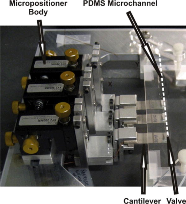
Image of the piezoelectrically actuated micropump showing the microvalves, cantilevers and micropositioners. The dashed line was added to show the position of the PDMS microchannel.
J) Software and Hardware
The cantilevers were actuated with square wave signals that were placed 120° out of phase, so as to create a peristaltic wave motion. The signals were created using a virtual function generator (National Instruments), which allowed for control of signal shape, frequency, amplitude, and phase. The generated signals were amplified with in-house fabricated external electronic hardware, where high-voltage amplifiers (Apex Microtechnology, PA15A) were used to amplify the virtual function generator signals to Vp = ±90V, which is the maximum driving potential for the cantilevers, as reported by the manufacturer.
Characterization Experiments
K) Flow Rate
Micropump flow rate values were obtained at specific frequencies by connecting the outlet capillary tube line of the micropump to an external piece of capillary tube ~1 m in length. The external piece of capillary tube was secured in place along a meter stick with mm ticks/gradations. The external capillary tube was filled with blue food dye solution prior to mating with the outlet line of the micropump. The blue dye provided greater contrast and easier tracking of a 2–3 mm bubble, which was intentionally introduced when the two capillary tubes were connected. Flow rate was calculated using the formula Q = Av, where “Q” represents the flow rate, “A” the cross-sectional surface area of the flow channel, and “v” the linear flow velocity of the bubble. All flow rates were calculated while actuating the micropump with a 120° square wave signal. The standard errors were calculated and plotted as error bars for each data set, where (n=4) for the SU-8 rectangular microchannel device, and (n=6) for the injection molded rounded/Gaussian shaped microchannel device.
L) Backpressure and Pressure Loss Measurements
Maximum attainable backpressure and valve leakage data were both obtained within a single experiment using the same setup. While being actuated, the micropump outlet capillary tube line was first connected to an electronic pressure sensor (Honeywell, 40PC015G2A). The injection molded micropump was actuated at 25 Hz, with the SU-8 REM micropump actuated at 60 Hz, where in both cases, the micropump was actuated until the maximum attainable backpressure had been attained, as indicated by the pressure sensor. After attaining this point, the micropump was stopped, with only one valve was left in the fully closed position. Pressure readings were recorded for 15 minutes to observe pressure loss within the system, where after this time the valve was fully opened. For each respective micropump, (n=3) experiments were performed.
M) Fluorescence Valve Closure Measurements
The micropump was placed in an inverted position under an epifluorescent microscope that was covered with a black cape, so as to block ambient light when taking measurements. All three microvalves were first placed in the fully open position under the microscope, where distilled water was next forced throughout the micropump channel using a syringe pump. The syringe pump was then turned off, where after 30 s, the micropump outlet line was capped off. After allowing the closed-off system to stabilize for 30 minutes, fully open and fully closed valve intensities were recorded with the epifluorscent microscope (Nikon, SMZ1500 with filter cube 470/440/500 nm – excitation/emission/long pass). Without disturbing the micropump in the inverted position, the micropump channel was next filled with a 10 mM fluorescein solution, where the same experiment was repeated as already described using distilled water. Background subtracted images were produced using Metavue, by subtracting the distilled water signal from the fluorescent recorded signal.
Results and Discussion
Injection Mold Wire-Template Channel
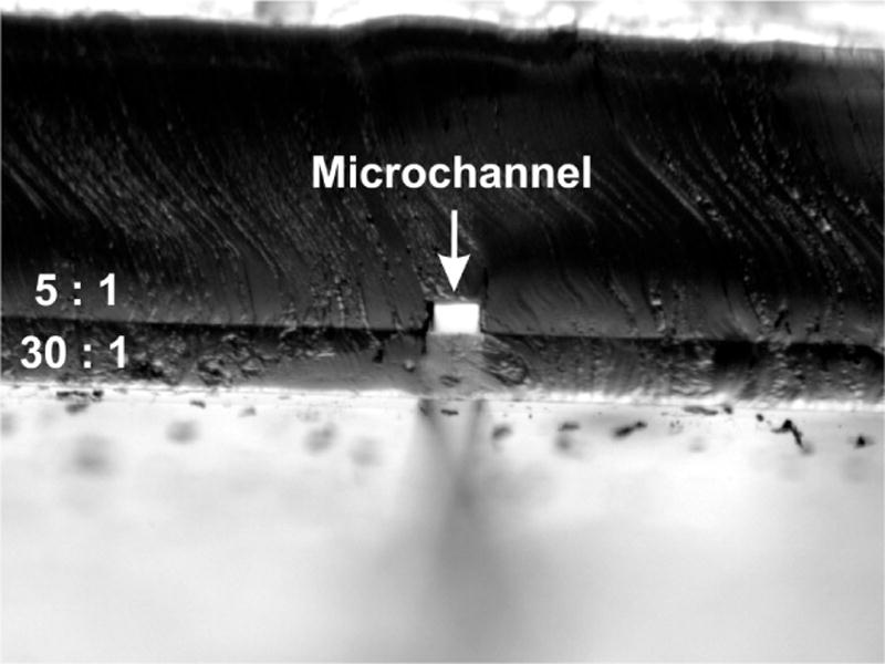
Figure 3 shows the microchannel cross-sectional geometry produced using the injection mold wire-template.
Fig. 3.
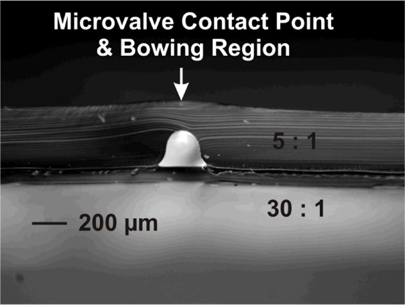
Cross-sectional image of microchannel geometry produced from injection mold wire-template. Template formed from aluminium foil and general purpose spray adhesive applied over a wire of diameter ~152 μm, and straddled across bottom plate of injection mold apparatus.
The overall height of the channel was measured as ~198 μm, where the 5 : 1 PDMS membrane directly over the channel was observed to be ~155 μm thick. The maximum width at the base of the channel was measured as ~272 μm. Further the overall 5 : 1 thickness was recorded as ~330 μm, with the overall thickness of the 30 : 1 layer recorded as ~85 μm. As seen within Figure 3, the wire molded cross-sectional channel geometry is very uniform/symmetric and resembles that of a Gaussian bell-shaped curve, where it has been shown how important this characteristic is for microfluidic valving operations. 63–65 One further point to note is the measured channel height taken to be ~198 μm, as compared to the wire molding template feature which possessed a height of ~152 μm. The discrepancy in part could be attributed to an increase in molding wire height, as a result of the general purpose spray adhesive and aluminum foil placed over the wire to form the template, however, at most 10–20 μm of added thickness would be expected for these additions. It can be seen within Figure 3 that the top surface of the membrane is slightly bowed, where it is believed this physical effect is what accounts for the bulk of the increase in channel height. This channel distortion could be introduced when the two PDMS layers are bonded to one another, where previously it has been shown how various PDMS geometries can be distorted, especially with high-aspect-ratio PDMS structures.72, 73 Other possible explanations to account for these observations, could be attributed in-part to PDMS shrinkage 1, 74 during the curing/bonding process, and/or possibly stemming in-part from the mismatch in PDMS channel height, as compared to the diameter of the capillary tube bonded within the microchannel.
Injection Mold CNC Machined Template Channel
Figure 4A shows a cross-sectional image of the CNC template molded microchannel geometry before 30 : 1 base layer bonding, where Figure 4B shows the geometry after 30 : 1 base layer bonding. The contrast between images shows a rather dramatic distortion in microchannel geometry after base layer bonding, where the channel height before bonding was measured as ~77 μm, and ~114 μm after bonding, with the channel width at the base (i.e. opposite the membrane) changing from ~65 μm to ~34 μm for before vs. after bonding, respectively. Therefore the aspect ratio taken as the ratio of channel height to channel width, changes from 1.2 to 3.4, representing a 2.8-fold overall change. This change in aspect ratio is likely due to the bowing effect as previously described for the wire template injection mold.
Fig. 4.
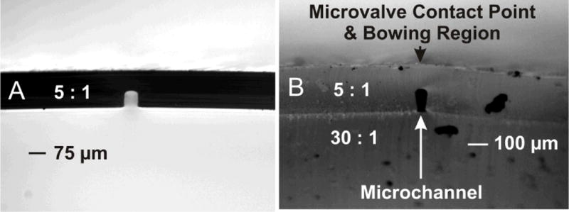
Side-by-side images of before and after bonding of 30 : 1 base layer, to 5 : 1 channel mold. Channel produced using CNC machined template and injection mold apparatus. Base layer bonding shows distortion of final cross-sectional channel geometry.
SU-8 REM Channel
Figure 5A shows a cross-sectional image of the SU-8 template molded microchannel geometry before bonding of the 30 : 1 base layer, with Figure 5B showing the geometry after bonding of the 30 : 1 base layer. The rather dramatic distortion in channel geometry can be seen to parallel the same effect as shown within Figure 4. The aspect ratio taken as the ratio of channel height/width (width measured at base of the microchannel, i.e. opposite the membrane) was measured as 40/88 μm for Figure 5A, and 57/57 μm for Figure 5B. This represents an overall 2.2-fold change in aspect ratio when the 30 : 1 base layer is bonded. These channel distortions are likely a result of the bowing effect, as described within the previous two sections.
Fig. 5.
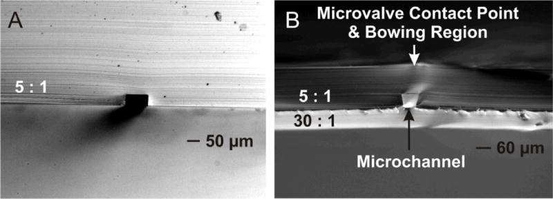
Side-by-side images of before and after bonding of 30 : 1 base layer, to 5 : 1 channel mold. Channel mold produced using SU-8 fabricated template. Bonding of base layer shows distortion of final cross-sectional channel geometry.
It should be noted, not all cross-sectional channel geometries were observed with channel distortions. Figure 6 shows a cross-sectional image of a microchannel fabricated using an SU-8 template, where the mask used was 50 μm in width. Before base layer bonding images were not captured, however channel dimensions after base layer bonding were measured as 41/66 μm for the channel height/width (width measured at the base of the microchannel, i.e. opposite the membrane), which represents a final aspect ratio of 0.62. Presumably, the microchannel aspect ratio was optimized before the 30:1 base layer was bonded. This hypothesis is consistent with previously discussed results for very high or very low aspect ratio PDMS microstructures.73 Microchannel distortions are also less likely to occur when the channel layer is fabricated from; 1) a 5 : 1 vs. a 30 : 1 PDMS ratio, and 2) an overall thicker piece of 5 : 1 PDMS, relatively speaking. A thicker PDMS slab and/or a 6-fold decrease in ratio of base/curing agent, would produce a much more rigid slab of PDMS, where the 5 : 1 slab of Figure 6 is shown to be much thicker in comparison to the 5 : 1 slabs as shown within Figures 4 and 5.
Fig. 6.
Cross-sectional channel geometry produced using an SU-8 template. Channel formed using a photolithography mask of width 50 μm. Image shows vertical channel sidewalls, and therefore an undistorted cross-sectional channel geometry produced after bonding of 30 : 1 base layer.
Valve Closure Image Data
An image of a fully open vs. fully closed microvalve can be seen in Figure 7. This image was recorded through the back side of the micropump, opposite the contact point of the microvalves. Fluorescein fluorescence is clearly visible along the length of the channels when in the open position. The darker areas near the middle of the open channel images show where the microvalves contact the PDMS. Fluorescein remains in the in the closed - SU-8 image, indicating the channel did not fully close along the bottom right edge of the microchannel (between the arrows). The operation and stability of the SU-8 REM micropump proved to be a challenging task, where the non-ideal cross-sectional channel geometry is the expected culprit for these operational challenges.
Fig. 7.
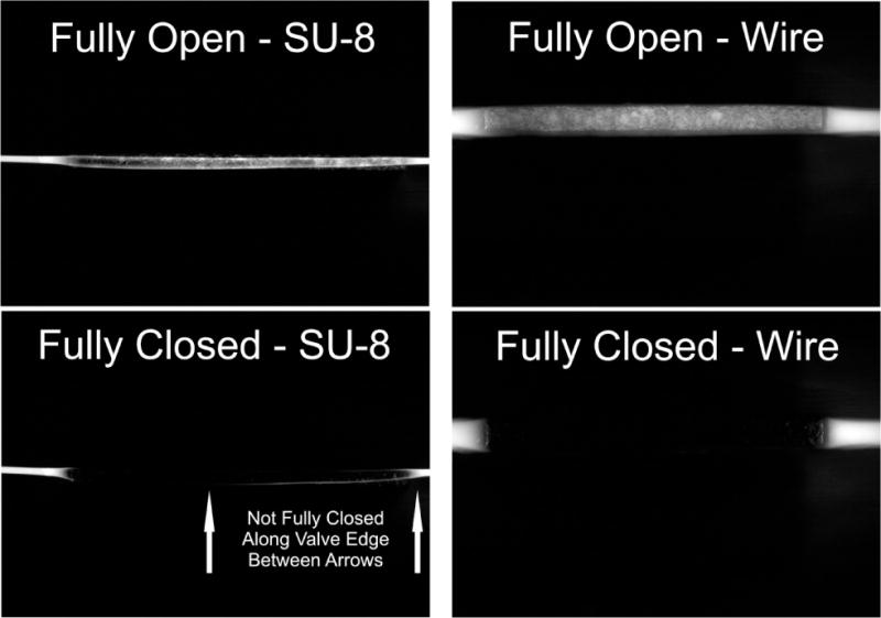
Images of valve closure for SU-8 and wire-template molded microchannels. Images taken with micropump placed in an inverted position under an epifluorescent microscope, with fluorescein trapped within the microchannels. Images are taken from the back side of the device (i.e. opposite the contact point of the microvalve contact point) with the channels run horizontaIly in the above images. Residual fluorescence remains in the compression region of the fully closed SU-8 molded channel, indicating incomplete closure of the channel. No fluorescence was observed in the compression region of the wire-molded channel indicatingull closure.
The wire-molded channel images are shown on the right side of Figure 7. As seen for the closed - wire image, the channel fully collapsed, where no fluorescein was recorded beneath the closed valve region. This micropump demonstrated stable operation, however several microvalve adjustments were necessary to ensure complete valve closure. Wire molded micropumps were also fabricated using wire with diameters of 55 μm, and 250 μm. The cantilevers were able to output just enough force to fully close the 250 μm channel, where operation was unstable. In contrast, the cantilevers had no trouble fully closing the 55 μm wire molded channel, however these pumps failed to produce a net flow. The peristaltic wave driving force was likely not sufficient to overcome this micropumps high internal flow resistance. These micropumps were fabricated with small inner diameter capillary tubes (90/20 μm, OD/ID), where it is known the hydraulic resistance for laminar flow through a rigid straight pipe, with circular cross-sectional channel geometry, scales as Rh ∝ 1/r4, for “Rh” equal to the hydraulic resistance, and “r” equal to the radius of the circular pipe.75–77
Backpressure and Pressure Loss Data
The backpressure data recorded for the two microchannel designs can be seen in Figure 8. Three experiments were performed for each design, where the average maximum backpressure recorded for the SU-8 micropump was 51.5 kPa, and 25.8 kPa for the wire molded micropump. When considering the valve closure data as shown within Figure 7, it might be expected the SU-8 template molded micropump would have a higher average pressure loss over the course of the first 15 minutes due to valve leakage, however this was not the case. The average pressure loss for the first 15 minutes with only one valve in the fully closed position was recorded to be 5.9% for the SU-8 molded micropump, and 6.1% for the wire molded channel. Previous micropump experience indicates this pressure loss can be nearly, if not fully, attributed to pressure loss through union connectors attached to the inlet and outlet lines of the micropump.
Fig. 8.
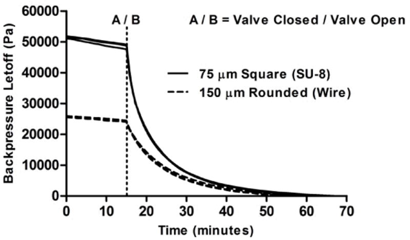
Plot of backpressure and valve leakage characteristics for SU-8 and wire-template molded microchannels. Plot shows nearly same pressure loss recorded over the time-course of the first 15 minutes, where one valve was left in the fully closed position. This initial pressure loss likely occurs through leaky capillary tube connectors, and not across the microvalve. An average maximum backpressure of 51.5 kPa and 25.8 kPa was recorded for the SU-8 and wire-molded micropumps, respectively. Three representative experiments were performed for each micropump design.
Flow Rate Data
The flow rate data collected for both micropump designs can be observed in Figure 9. Up to approximately 20 Hz, the flow curves are very similar in nature. Past this frequency however, the flow curves diverge, where the error bars illustrate how the flow rates become slightly erratic at higher frequencies for the SU-8 molded micropump. The flow rates for the wire template molded micropump however, remain quite stable throughout the entire range of characterized actuation frequencies. The unstable SU-8 micropump curve is likely explained in large part based upon the non-ideal rectangular cross-sectional channel geometry. Figure 10 is a plot of standard errors vs. frequency, for the SU-8 vs. wire molded microchannels, to further highlight the instability of the SU-8 micropump, compared to that of the wire molded micropump. The range of average flow rates for the SU-8 micropump design was 33 – 159 nL/min (0.3 – 60 Hz), and 44 – 119 nL/min (0.1 – 60 Hz) for the wire molded micropump design.
Fig. 9.
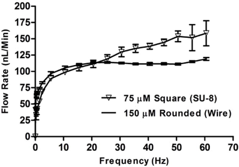
Data shown for flow rate vs. frequency for SU-8 and wire-molded micropump designs. Data shows flow rate characteristics for the micropumps is very similar up to around 20 Hz, where thereafter the data becomes slightly unstable for the SU-8 micropump, but continues to increase to an average maximum flow rate of 159 nL/min. An average maximum flow rate of 119 nL/min was recorded for the wire-molded micropump. Error bars represent the standard error of the mean (n = 4 for SU-8 micropump, n = 6 for wire-molded micropump).
Fig. 10.
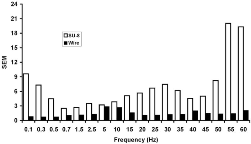
Plot of standard errors for flow rate vs. frequency. Comparison is made for SU-8 vs. wire molded microchannels, for the data presented within Figure 8. Plot shows the flow rate instability of the square (SU-8) vs. rounded/Gaussian (wire molded) shaped microchannel geometries. These data suggest that piezoelectrically actuated micropumps are particularly sensitive to channel geometry and operate much more robustly using rounded channels.
Conclusions
The current work characterized the differences in two micropump fabrication methods, using; 1) SU-8 replica molding, and 2) micro injection molding. The two respective designs produced two very disparate cross-sectional channel geometries, with the SU-8 process producing a rectangular geometry, and the injection mold producing a Gaussian/rounded geometry. Both pump designs produce a net flow, however operation of the SU-8 pump was less stable in comparison to the injection molded micropump. Microchannel geometry distortion was characterized both before and after 30 : 1 base layer bonding. It was shown in some instances, distortion can be rather extreme when comparing the initial (before base layer bonding) vs. final (after base layer bonding) cross-sectional channel geometries. The injection molding process was shown to be a very simple, cheap, fast, and reproducible fabrication process, far superior to the sandwich molding process used to fabricate the SU-8 micropumps. The injection molding apparatus is also very unique compared to many other commercial injection molding machines, where the current disclosed apparatus is handheld, and additionally designed for use with RTV polymers, as opposed to the more commonly used thermoplastic polymers.
Acknowledgments
We would like to acknowledge the contributions of Dave Hultman and co-workers at the University of Minnesota Electrical Engineering Machine Shop, for their efforts directed to the injection mold. We would further like to acknowledge the NanofabricationCenter at the University of Minnesota, and NNIN’s support of NFC. This research was supported by NIH grant NS043304.
References
- 1.Xia Y, Whitesides GM. Angewandte Chemie, International Edition. 1998;37:550–575. doi: 10.1002/(SICI)1521-3773(19980316)37:5<550::AID-ANIE550>3.0.CO;2-G. [DOI] [PubMed] [Google Scholar]
- 2.Manz A, Graber N, Widmer HM. Sensors and Actuators B: Chemical. 1990;1:244–248. [Google Scholar]
- 3.Harrison DJ, Fluri K, Seiler K, Fan Z, Effenhauser CS, Manz A. Science. 1993;261:895–897. doi: 10.1126/science.261.5123.895. [DOI] [PubMed] [Google Scholar]
- 4.Campbell SA. The Science and Engineering of Microelectronic Fabrication. Oxford: 2001. [Google Scholar]
- 5.Madou MJ. Fundamentals of Microfabrication – The Science of Miniaturization. CRC Press; 2002. [Google Scholar]
- 6.Senturia SD. Microsystems Design. Kluwer Academic Publishers; 2001. [Google Scholar]
- 7.Kovacs GTA. Micromachined Transducers Sourcebook. McGraw Hill; New York, New York: 1998. [Google Scholar]
- 8.Abgrall P, Conedera V, Camon H, Gue AM, Nguyen NT. Electrophoresis. 2007;28:4539–4551. doi: 10.1002/elps.200700333. [DOI] [PubMed] [Google Scholar]
- 9.Sikanen T, Tuomikoski S, Ketola RA, Kostiainen R, Franssila S, Kotiaho T. Lab on a Chip. 2005;5:888–896. doi: 10.1039/b503016a. [DOI] [PubMed] [Google Scholar]
- 10.Campo Ad, Greiner C. Journal of Micromechanics and Microengineering. 2007;17:R81. [Google Scholar]
- 11.Keller S, et al. Journal of Micromechanics and Microengineering. 2008;18:125020. [Google Scholar]
- 12.Zhang J, Chan-Park MB, Conner SR. Lab on a Chip. 2004;4:646–653. doi: 10.1039/b403304c. [DOI] [PubMed] [Google Scholar]
- 13.Wouters K, Puers R. Journal of Micromechanics and Microengineering. 2010;20:095013. [Google Scholar]
- 14.Zhang J, et al. Journal of Micromechanics and Microengineering. 2001;11:20. [Google Scholar]
- 15.Choi KM. Journal of Physical Chemistry B. 2005;109:21525–21531. doi: 10.1021/jp050302t. [DOI] [PubMed] [Google Scholar]
- 16.Mukhopadhyay R. Analytical Chemistry. 2007;79:3248–3253. doi: 10.1021/ac071903e. [DOI] [PubMed] [Google Scholar]
- 17.McDonald JC, Whitesides GM. Accounts of Chemical Research. 2002;35:491–499. doi: 10.1021/ar010110q. [DOI] [PubMed] [Google Scholar]
- 18.Duffy DC, McDonald JC, Schueller OJA, Whitesides GM. Analytical Chemistry. 1998;70:4974–4984. doi: 10.1021/ac980656z. [DOI] [PubMed] [Google Scholar]
- 19.Heckele M, Schomburg WK. Journal of Micromechanics and Microengineering. 2004;14:R1–R14. [Google Scholar]
- 20.Becker H, Locascio LE. Talanta. 2002;56:267–287. doi: 10.1016/s0039-9140(01)00594-x. [DOI] [PubMed] [Google Scholar]
- 21.Abgrall P, Gue AM. Journal of Micromechanics and Microengineering. 2007;17:R15–R49. [Google Scholar]
- 22.Becker H, Gartner C. Analytical & Bioanalytical Chemistry. 2008;390:89–111. doi: 10.1007/s00216-007-1692-2. [DOI] [PubMed] [Google Scholar]
- 23.Becker H, Gartner C. Electrophoresis. 2000;21:12–26. doi: 10.1002/(SICI)1522-2683(20000101)21:1<12::AID-ELPS12>3.0.CO;2-7. [DOI] [PubMed] [Google Scholar]
- 24.Quinn DJ, Spearing SM, Ashby MF, Fleck NA. Journal of Microelectromechanical Systems. 2006;15:1039–1050. [Google Scholar]
- 25.Koesdjojo MT, Tennico YH, Remcho VT. Analytical Chemistry. 2008;80:2311–2318. doi: 10.1021/ac7021647. [DOI] [PubMed] [Google Scholar]
- 26.Pemg BY, Wu CW, Shen YK, Lin Y. Polymers for Advanced Technologies. 2010;21:457–466. [Google Scholar]
- 27.Li JM, et al. Journal of Micromechanics and Microengineering. 2008;18:015008. doi: 10.1088/0960-1317/18/4/045015. [DOI] [PMC free article] [PubMed] [Google Scholar]
- 28.Mehta G, Lee J, Cha W, Tung YC, Linderman JJ, Takayama S. Analytical Chemistry. 2009;81:3714–3722. doi: 10.1021/ac802178u. [DOI] [PubMed] [Google Scholar]
- 29.Gustafsson O, Mogensen KB, Kutter JP. Electrophoresis. 2008;29:3145–3152. doi: 10.1002/elps.200800131. [DOI] [PubMed] [Google Scholar]
- 30.Martynova L, Locascio LE, Gaitan M, Kramer GW, Christensen RG, MacCrehan WA. Analytical Chemistry. 1997;69:4783–4789. doi: 10.1021/ac970558y. [DOI] [PubMed] [Google Scholar]
- 31.Liu HB, Gong HQ. Journal of Micromechanics and Microengineering. 2009;19:037002. [Google Scholar]
- 32.Grzybowski BA, Haag R, Bowden N, Whitesides GM. Analytical Chemistry. 1998;70:4645–4652. [Google Scholar]
- 33.Fogarty BA, Heppert KE, Cory TJ, Hulbutta KR, Martin RS, Lunte SM. The Analyst. 2005;130:924–930. doi: 10.1039/b418299e. [DOI] [PubMed] [Google Scholar]
- 34.Klank H, Kutter JP, Geschke O. Lab on a Chip. 2002;2:242–246. doi: 10.1039/b206409j. [DOI] [PubMed] [Google Scholar]
- 35.Chaitanya CRA, Takahata K. Journal of Micromechanics and Microengineering. 2008;18:105009. [Google Scholar]
- 36.Chen CHB, Dellamaggiore KR, Ouellette CP, Seclano CD, Lizadjohry M, Chernis GA, Gonzales M, Baltasar FE, Fan AL, Myerowitz R, Neufeld EF. Proceedings of the National Academy of Sciences of the United States of America. 2008;105:15908–15913. doi: 10.1073/pnas.0808360105. [DOI] [PMC free article] [PubMed] [Google Scholar]
- 37.Chen S-T, et al. Journal of Micromechanics and Microengineering. 2009;19:115033. [Google Scholar]
- 38.Natali M, Begolo S, Carofiglio T, Mistura G. Lab on a Chip. 2008;8:492–494. doi: 10.1039/b716594c. [DOI] [PubMed] [Google Scholar]
- 39.Paul D, Pallandre A, Miserere S, Weber J, Viovy JL. Electrophoresis. 2007;28:1115–1122. doi: 10.1002/elps.200600503. [DOI] [PubMed] [Google Scholar]
- 40.Martin PM, Matson DW, Bennett WD, Lin Y, Hammerstrom DJ. Journal of Vacuum Science & Technology A. 1999;17:2264–2269. [Google Scholar]
- 41.Wilson ME, Kota N, Kim Y, Wang Y, Stolz DB, LeDuc PR, Ozdoganlar OB. Lab on a Chip. 2011;11:1550–1555. doi: 10.1039/c0lc00561d. [DOI] [PubMed] [Google Scholar]
- 42.Mecomber JS, Stalcup AM, Hurd D, Halsall HB, Heineman WR, Seliskar CJ, Wehmeyer KR, Limbach PA. Analytical Chemistry. 2005;78:936–941. doi: 10.1021/ac051523y. [DOI] [PubMed] [Google Scholar]
- 43.McDonald JC, Chabinyc ML, Metallo SJ, Anderson JR, Stroock AD, Whitesides GM. Analytical Chemistry. 2002;74:1537–1545. doi: 10.1021/ac010938q. [DOI] [PubMed] [Google Scholar]
- 44.Xia C, Fang N. Biomedical Microdevices. 2009;11:1309–1315. doi: 10.1007/s10544-009-9350-4. [DOI] [PubMed] [Google Scholar]
- 45.Snowden ME, King PH, Covington JA, Macpherson JV, Unwin PR. Analytical Chemistry. 2010;82:3124–3131. doi: 10.1021/ac100345v. [DOI] [PubMed] [Google Scholar]
- 46.Conrad PG, II, Nishimura PT, Aherne D, Schwartz BJ, Wu D, Fang N, Zhang X, Roberts MJ, Shea KJ. Advanced Materials. 2003;15:1541–1544. [Google Scholar]
- 47.Giboz J, et al. Journal of Micromechanics and Microengineering. 2007;17:R96. [Google Scholar]
- 48.Attia U, Marson S, Alcock J. Microfluidics and Nanofluidics. 2009;7:1–28. [Google Scholar]
- 49.Hansen TS, et al. Journal of Micromechanics and Microengineering. 2010;20:015020. [Google Scholar]
- 50.Fu G, et al. Journal of Micromechanics and Microengineering. 2010;20:085019. [Google Scholar]
- 51.Kim DS, Lee SH, Ahn CH, Lee JY, Kwon TH. Lab on a Chip. 2006;6:794–802. doi: 10.1039/b516495h. [DOI] [PubMed] [Google Scholar]
- 52.Utko P, Persson F, Kristensen A, Larsen NB. Lab on a Chip. 2011;11:303–308. doi: 10.1039/c0lc00260g. [DOI] [PubMed] [Google Scholar]
- 53.Attia U, Alcock J. The International Journal of Advanced Manufacturing Technology. 2010;48:973–991. [Google Scholar]
- 54.Han A, Wang O, Graff M, Mohanty SK, Edwards TL, Han KH, Frazier AB. Lab on a Chip. 2003;3:150–157. doi: 10.1039/b302118a. [DOI] [PubMed] [Google Scholar]
- 55.Steigert J, et al. Journal of Micromechanics and Microengineering. 2007;17:333. [Google Scholar]
- 56.Kim S, et al. Journal of Micromechanics and Microengineering. 2010;20:015037. [Google Scholar]
- 57.Kim SJ, Yang H, Kim K, Lim YT, Pyo HB. Electrophoresis. 2006;27:3284–3296. doi: 10.1002/elps.200500773. [DOI] [PubMed] [Google Scholar]
- 58.Damean N, Regtien PPL. Sensors and Actuators A: Physical. 2001;90:96–101. [Google Scholar]
- 59.Ajdari A, Bontoux N, Stone HA. Analytical Chemistry. 2005;78:387–392. doi: 10.1021/ac0508651. [DOI] [PubMed] [Google Scholar]
- 60.Squires TM, Quake SR. Reviews of Modern Physics. 2005;77:977–1026. [Google Scholar]
- 61.Kreutzer MT, Gunther A, Jensen KF. Analytical Chemistry. 2008;80:1558–1567. doi: 10.1021/ac702143r. [DOI] [PubMed] [Google Scholar]
- 62.Futai N, Gu W, Takayama S. Advanced Materials. 2004;16:1320–1323. [Google Scholar]
- 63.Unger MA, Chou HP, Thorsen T, Scherer A, Quake SR. Science. 2000;288:113–116. doi: 10.1126/science.288.5463.113. [DOI] [PubMed] [Google Scholar]
- 64.Graf NJ, Bowser MT. Lab on a Chip. 2008;8:1664–1670. doi: 10.1039/b805252b. [DOI] [PMC free article] [PubMed] [Google Scholar]
- 65.Park W, Han S, Kwon S. Lab on a Chip. 2010;10:2814–2817. doi: 10.1039/c005173j. [DOI] [PubMed] [Google Scholar]
- 66.Abdelgawad M, Wu C, Chien WY, Geddie WR, Jewett MAS, Sun Y. Lab on a Chip. 2011;11:545–551. doi: 10.1039/c0lc00093k. [DOI] [PubMed] [Google Scholar]
- 67.Wang GJ, Ho KH, Hsu SH, Wang KP. Biomedical microdevices. 2007;9:657–663. doi: 10.1007/s10544-007-9067-1. [DOI] [PubMed] [Google Scholar]
- 68.Park J, Kim DH, Kim G, Kim Y, Choi E, Levchenko A. Lab on a Chip. 2010;10:2130–2138. doi: 10.1039/b924222h. [DOI] [PubMed] [Google Scholar]
- 69.Wen J, Albrecht JW, Jensen KF. Electrophoresis. 2010;31:1606–1614. doi: 10.1002/elps.200900577. [DOI] [PMC free article] [PubMed] [Google Scholar]
- 70.Kumi G, Yanez CO, Belfield KD, Fourkas JT. Lab on a Chip. 2010;10:1057–1060. doi: 10.1039/b923377f. [DOI] [PubMed] [Google Scholar]
- 71.Graf N, Bowser M. Submitted for Publication. 2011 [Google Scholar]
- 72.Rogers JA, Paul KE, Whitesides GM. Journal of Vacuum Science & Technology, B: Microelectronics and Nanometer Structures. 1998;16:88–97. [Google Scholar]
- 73.Qin D, Xia Y, Whitesides GM. Nature Protocols. 2010;5:491–502. doi: 10.1038/nprot.2009.234. [DOI] [PubMed] [Google Scholar]
- 74.Moraes C, et al. Journal of Micromechanics and Microengineering. 2009;19:065015. [Google Scholar]
- 75.Young DF, Munson BR, Okiishi TH. A Brief Introduction to Fluid Mechanics. John Wiley & Sons, Inc.; 2004. [Google Scholar]
- 76.Kirby BJ. Micro- and Nanoscale Fluid Mechanics. Cambridge University Press; 2010. [Google Scholar]
- 77.Bruus H. Theoretical Microfluidics. Oxford University Press; 2008. [Google Scholar]