Abstract
We demonstrate a 3-D scanning micromirror device that combines 2-D beam scanning with focus control in the same device using micro-electro-mechanical-systems (MEMS) technology. 2-D beam scanning is achieved with a biaxial gimbal structure and focus control is obtained with a deformable mirror membrane surface. The micromirror with 800 micrometer diameter is designed to be sufficiently compact and efficient so that it can be incorporated into an endoscopic imaging probe in the future. The design, fabrication and characterization of the device are described in this paper. Using the focus-tracking MEMS scanning mirror, we achieved an optical scanning range of >16 degrees with <40 V actuation voltage at resonance and a tunable focal length between infinity and 25 mm with <100V applied bias.
OCIS codes: (170.2150) Endoscopic imaging, (230.0230) Optical devices, (230.4685) Optical microelectromechanical devices
1. Introduction
Endoscopic imaging has been, and continues to be an important diagnostic tool in biomedicine [1]. Current clinical endoscopy offers a magnified view of the epithelial surface but is not capable of imaging subepithelial morphology. Advanced optical imaging technologies such as scanning confocal microscopy [2], optical coherence tomography (OCT) [3], and multiphoton microscopy [4] are non-invasive and capable of in vivo assessment of tissue microanatomy below the epithelial surface in real time at resolutions (~0.5-10 µm) approaching those of conventional histological techniques. Combining these imaging techniques with endoscopy can therefore greatly improve its capability.
All three optical imaging techniques described above require mechanisms to deliver, focus, scan and collect a single-mode optical beam. Although it is possible to deliver an optical beam to internal organs using a single-mode optical fiber, the integration of beam scanning, focusing and collection using an imaging probe of only a few millimeters in diameter is a major engineering challenge. A second challenge is the need for a focus-tracking mechanism to maintain a high transverse resolution at varying depths, but integrating focus-tracking mechanisms with miniature scanning imaging probes have not been fully explored. Although piezoelectric-actuated scanning optical fibers have been utilized for OCT and two-photon fluorescence endoscopy, and impressive imaging results have been demonstrated [5-9], a miniature imaging probe capable of raster scanning with dynamic focus-tracking remains attractive [10].
Due to the capability of integrating complex functionality in small devices, MEMS technologies have been explored to develop scanning devices for endoscopic imaging. Vertical comb-drive actuated micromirrors [11, 12] and magnetically-driven micromirrors [13] can achieve linear scanning, but these actuator structures occupy a significant amount of space. A 2-D electrothermal micromirror with 2 × 2 mm2 device footprint has also been demonstrated [14]. However the electrothermal actuation mechanism requires electrical power and is slower in nature. None of these scanning devices can perform focus-tracking simultaneously. A deformable mirror membrane can be utilized to achieve this goal, and a scanning deformable mirror has been proposed and fabricated for confocal scanning laser microscopy and Doppler OCT [15, 16]. Here, we propose and demonstrate a 2-D MEMS scanning mirror with a tunable mirror radius of curvature based on a similar approach. The micromirror achieves spatial beam steering using a bi-axial gimbal structure to scan the image en face and focal length control to dynamically change the depth of the scan. The gap-closing electrostatic actuation mechanisms for both scanning and focus control allow small device footprint of 1.5 × 1.5 mm2 for integration with an endoscopy imaging channel. An optical scanning range of >16 degrees can be achieved with 40V actuation voltage at resonance. Focal length tunability between infinity and 25 mm can also be obtained with <100V applied bias.
2. Device Design and Fabrication
The MEMS micromirror was designed to fit inside the working channel of a standard endoscope (<3 mm). This size limitation and the necessary optical, electrical and mechanical performance parameters dictated many aspects of the design. Figure 1 shows the 3-D cross-sectional schematic drawing of the micromirror and the electrode pillar underneath which is fabricated on a separate wafer. The mirror surface consists of a silicon nitride membrane with a gold reflective layer suspended over a silicon frame. This device employs a gimbal structure to allow 2-D tilting of the mirror. To maximize the area of the mirror while minimizing the die area, the tilt and focus of the mirror are controlled electrostatically with a set of six electrodes since they do not require additional structures like comb drive that occupy large space. The mirror surface and the silicon layer underneath act as two electrodes to control the curvature of the membrane. Four electrodes placed beneath the mirror are used for scanning actuation. During testing of the mirror, the silicon frame beneath the mirror is always grounded while other electrodes are charged to produce the electric field. In order to reduce the effect of interference between the scanning operation and the curvature control when both are actuated simultaneously, the polarity of the voltage used is matched. While allowing large electric fields to be generated between the desired electrodes, this configuration helps to minimize other undesired effects. The mirror is designed to be as large as possible (800 µm in diameter) for maximizing the deliverable beam size while still maintaining a small package size.
Fig. 1.
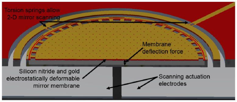
3-D cross-sectional view of the MEMS scanning micromirror with focus control.
The fabrication process for the MEMS micromirrors is a five-photomask process that starts with a bare silicon wafer polished on both sides and highly doped with phosphorous for good electrical conductivity. The wafer is then thermally oxidized and the 600 nm-thick silicon oxide layer is patterned to form the sacrificial layers beneath each mirror [Fig. 2(a) ]. Low pressure chemical vapor deposition (LPCVD) is used to deposit the 500 nm-thick silicon nitride membrane layer which covers the entire wafer uniformly [Fig. 2(b)]. The nitride on the backside of the wafer is then patterned with the second photomask and deep (~470 µm) holes are etched into the wafer using potassium hydroxide (KOH), an anisotropic silicon etchant [Fig. 2(c)]. These holes reduce the thickness of the bulk silicon layer to about 30 µm thick at the location of each mirror. The next photomask defines the electrical vias that allow conductive metal layers to be connected to the silicon frame beneath the mirror. This pattern is etched through the silicon nitride to the silicon. A 200 nm-thick gold metal layer is sputtered on the wafer with the help of an adhesive chrome layer after a short argon plasma treatment [Fig. 2(d)]. The argon plasma serves two purposes, to remove any native oxide that may remain on the silicon and to roughen the wafer’s surface to promote the adhesion of the metal layer. The fourth photomask defines the electrical conductive layer patterns on the wafer. The last photomask for the device fabrication defines the trenches creating the gimbal and the etch vias in the surface of the mirror. After this lithography step the metal layers are etched and the pattern is transferred into the nitride layer using reactive ion etching (RIE). Deep reactive ion etching (DRIE) is used to define the gimbal structure by etching the same pattern 20 μm into the silicon. The photoresist is removed after this etching step. During the DRIE etching, the differing etch rates between silicon oxide and silicon allow the sacrificial silicon oxide layer beneath the membrane to protect the underlying silicon. Final release of the devices consists of two steps. The first step is etching the sacrificial oxide layer under the nitride membrane using hydrofluoric acid (HF) [Fig. 2(e)]. This is followed by using KOH to enlarge the cavity beneath the membrane and completely release the device by finishing the through-wafer etch and undercutting the torsion springs. A cross-sectional view of the final released devices is shown in the upper half of Fig. 2(f). A scanning electron microscope (SEM) image of the device is shown in Fig. 3(a) . The thicknesses of the mirror and the gimbal for the finished devices are about 20 μm, and the cavity beneath the mirror is ~4 μm deep. While the thickness of the tethers of the device was defined by the silicon nitride thickness (500 nm), variations of the width of the tethers between 10 μm and 40 μm allowed slight device tunability.
Fig. 2.
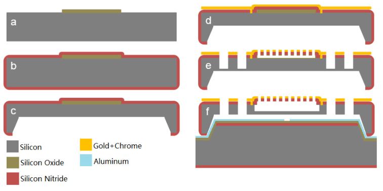
Fabrication process flow for the micromirror. (a) Silicon oxide pads are deposited and patterned. (b) LPCVD silicon nitride deposition. (c) Backside KOH etch. (d) Vias are created and the surface is metallized. (e) Pattern the metal layers and transfer the pattern into the nitride layer using RIE. Trenches are etched with DRIE. (f) Final release in HF and KOH, and align with the bottom electrode wafer.
Fig. 3.
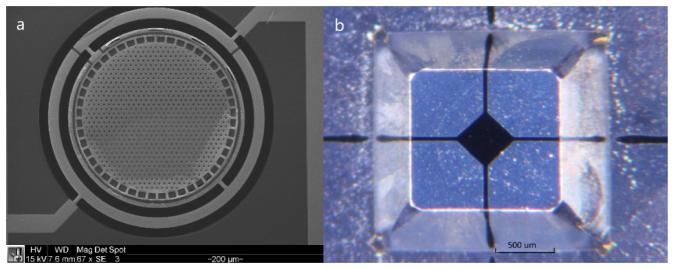
(a) A scanning electron microscopy image of the micromirror. (b) An optical microscopy image of the electrode pillar.
The electrode pillars are fabricated through a two-mask process that begins with a 1 mm-thick silicon wafer. A 200 nm-thick silicon nitride layer is deposited on both sides of the wafer using PECVD. This nitride layer acts as an etch mask for the bulk KOH etching while also protecting the back side of the wafer. Due to the anisotropic nature of KOH etching, the etch pattern used (first photomask) includes corner compensation to ensure the desired pillar shape after etching. This pattern is then transferred into the silicon nitride using RIE and after the resist is removed, KOH is used to etch the wafer, leaving ~400 μm-tall silicon pillars. A 2 µm-thick silicon oxide layer is then deposited using PECVD. This oxide layer serves as the insulating layer between the wafer and the 400 nm-thick aluminum electrode layer that is evaporated onto the surface. Spray-coating allows photoresist coverage on the sidewalls of the pillars and a second photomask is used to pattern the electrodes. The aluminum is etched in a commercially available wet etchant. The cross-sectional drawing of the electrode pillar wafer is shown in the lower part of Fig. 2(f). An optical microscopy image of the electrode pillar is shown in Fig. 3(b). The final device is assembled by aligning and inserting the pillar into the cavity under the micromirror device [Fig. 2(f)].
3. Results and Discussion
Several aspects of the performance of our micromirror devices were tested. The mechanical resonant frequency of the micromirror was measured to be ~216 Hz. Characterization of the scanning performance of the mirrors both with DC actuation and at resonance are performed by measuring the angular deflection of the mirror versus input actuation voltages. Figure 4 shows the measurement results. Static actuation results in a typical non-linear mechanical deflection versus applied voltage curve for gap-closing electrostatic actuated devices [Fig. 4(a)], while the result is linear under resonant actuation [Fig. 4(b)]. For endoscopic imaging, the MEMS mirror will be operated under resonance. An optical scanning angle of >16 degrees, corresponding to > ± 4 degrees mechanical scanning range, is demonstrated for this device with low actuation voltage (40 V).
Fig. 4.
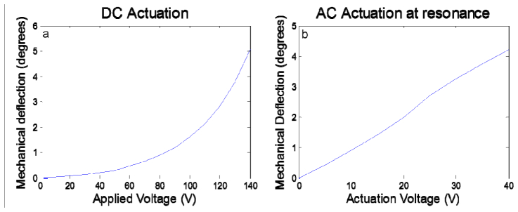
Angular deflection of the micromirror with (a) DC actuation, and (b) AC actuation at resonance. These curves show the response with the scanning axis defined by the inner torsion beams. Due to similar electrode and torsion beam geometries, the response of scanning in the other direction defined by the outer torsion beams is nearly identical.
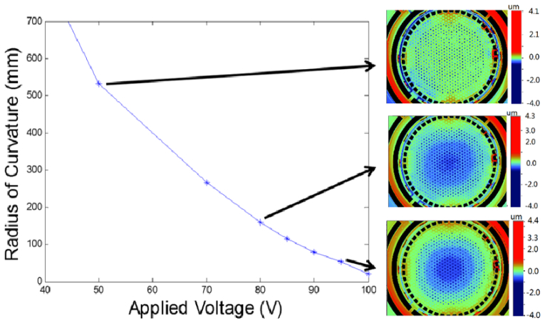
Measurement of radius-of-curvature change of the mirror membrane surface under various actuation conditions allows characterization of the focal length control of the mirror. The mirror membrane deflection is achieved by grounding the silicon frame and applying voltage to the mirror surface. Accurate mapping and measurement of the deflected mirror membrane was achieved using a Veeco HD 3300 optical surface profiler. The membrane deflection data generated from these surface scans allows the radius-of-curvature of the mirror to be calculated geometrically using spherical mirror approximation. As can be seen in Fig. 5 , between 50V and 95V, the membrane shows significant deflection indicated by the color in the center of the mirror where darker blue indicates greater deflection. It was also observed that the deflection is uniformly distributed across the mirror which is important for high optical beam quality. A large focus-control range was achieved with the radius-of-curvature tunable from infinity to 50 mm with <100V actuation. While not tested the dynamic performance of the curvature control is expected to be much greater than design requirements due to the small motion range and the actuation mechanism.
Fig. 5.
Experimental results of the radius-of-curvature control via applying voltage between the mirror membrane and the Si frame underneath. Three corresponding optical surface profiler images at 50 V, 80 V, and 95 V applied bias are also shown.
In order for these devices to be usable in an optical imaging system, the quality of the reflected optical beam must be characterized. A 675 nm collimated laser beam is used together with an optical beam profiler to measure the cross-sectional intensity profile of the focused spot and compare it to the intensity distribution of an ideal Gaussian beam. As shown in Fig. 6 , the intensity profile of the reflected beam fits well to an ideal Gaussian beam. The correlation with an ideal Gaussian beam increases with higher mirror membrane deflection. A correlation >95% can be achieved with maximum mirror membrane deflection. This correlation factor is calculated by the software of the beam profiler (Newport LPB-3-USB) as a percentage that is related to the integral of the difference between the gathered data and an ideal Gaussian curve squared compared to the integral of the ideal Gaussian curve squared.
Fig. 6.
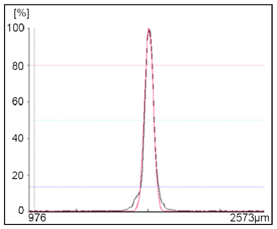
The intensity profile of the beam spot focused by the MEMS micromirror (black) with 87V applied voltage and the fitted ideal Gaussian beam profile (red). Greater than 95% correlation was achieved. This focused spot had a full-width-half-maximum (FWHM) of 68 μm.
The focal length tunability and focus spot size change by the MEMS micromirror were also characterized. Figure 7(a) shows the focal length control of an optical system with a lens of low numerical aperture (N.A. = 0.5) after the micromirror. A focal length tuning range of 250 µm was achieved with an applied voltage range of 50 V to 95 V between the mirror membrane and the Si frame. Figure 7(b) shows the focus spot size versus applied voltages. Figure 7(c) shows the intensity profile of a collimated input optical beam after reflection from the deflected mirror membrane with varying actuation voltages. With a collimated incident beam covering the entire mirror the beam can be focused to a spot as small as 68 μm with no additional optical components. Figure 7(d) shows the beam profile of the focused spot, which fits Gaussian profile well. When the optical system includes an additional focusing lens with a numerical aperture of 0.85, the size of the focused spot can be reduced to as little as 5 μm. While this additional lens decreases the focused spot size, the achievable range of focal length control of the system is also decreased. In an imaging system this lens must therefore be chosen to best achieve the goals of the specific system.
Fig. 7.
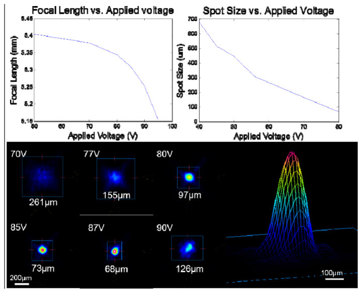
Experimental results of (a) focal length vs. applied voltage and (b) focused beam spot size vs. applied voltage between the mirror membrane and the Si frame. (c) Intensity cross-section of the optical beam at various applied voltages and (d) Gaussian intensity profile of the focused spot at 87 V bias, measured by an optical beam profiler.
The performance parameters, maximum scanning frequency, scanning range and focal length control together with the device size are critical for the incorporation of the micromirror into an imaging system. The maximum scanning frequency of the device relates to the mechanical resonant frequency and determines the frame rate of the imaging system. The range of scanning and focal length control determine the 3-dimensional field of view of the imager. Optimizing the device design for one parameter often involves trade-off with the other parameters. For example, increase in the resonant frequency can be achieved by altering the torsion spring design and increasing the spring constant. This, however, will also increase the necessary actuation voltages and potentially limit the maximum achievable scanning angle. Modifications to the design of the micromirrors could provide control over most of these important device parameters. Changing the balance of the parameters would allow this design to be optimized for different imaging systems.
4. Summary
We designed, fabricated and tested a MEMS scanning micromirror with tunable focal length through electrostatic actuation. ± 5 degrees of DC mechanical scan range was achieved with low actuation voltages. Also, mirror membrane deflection allowed a large range of focal length control between infinite and 25 mm with actuation voltage up to 100 V. Good Gaussian optical beam performance was maintained throughout the focus tuning. These attributes allow 3-dimensional control of the focal spot, which can greatly enhance the performance and capability of endoscopic optical imaging systems. Optical imaging experiments incorporating the focus-tracking MEMS scanning micromirror are currently underway.
Acknowledgments
This work is supported by the National Institutes of Health (Grant # R01 EB007636). Fabrication of the MEMS devices was mostly performed in the Microfabrication Facility at the University of Washington.
References and links
- 1.D. Provenzale, “Screening and surveillance of gastrointestinal cancers,” in Gastrointestinal Cancers, A. Rustgi and J. M. Crawford, eds. (Saunders Publishing, 2003), 193–204. [Google Scholar]
- 2.J. B. Pawley, Handbook of Biological Confocal Microscopy (Plenum Press, 1995). [Google Scholar]
- 3.Huang D., Swanson E. A., Lin C. P., Schuman J. S., Stinson W. G., Chang W., Hee M. R., Flotte T., Gregory K., Puliafito C. A., Fujimoto J. G., “Optical coherence tomography,” Science 254(5035), 1178–1181 (1991). 10.1126/science.1957169 [DOI] [PMC free article] [PubMed] [Google Scholar]
- 4.Denk W., Strickler J. H., Webb W. W., “Two-photon laser scanning fluorescence microscopy,” Science 248(4951), 73–76 (1990). 10.1126/science.2321027 [DOI] [PubMed] [Google Scholar]
- 5.Liu X., Cobb M. J., Chen Y., Kimmey M. B., Li X., “Rapid-scanning forward-imaging miniature endoscope for real-time optical coherence tomography,” Opt. Lett. 29(15), 1763–1765 (2004). 10.1364/OL.29.001763 [DOI] [PubMed] [Google Scholar]
- 6.Xi J. F., Chen Y. P., Zhang Y. Y., Murari K., Li M.-J., Li X. D., “Integrated multimodal endomicroscopy platform for simultaneous en face optical coherence and two-photon fluorescence imaging,” Opt. Lett. 37(3), 362–364 (2012). 10.1364/OL.37.000362 [DOI] [PMC free article] [PubMed] [Google Scholar]
- 7.Lee C. M., Engelbrecht C. J., Soper T. D., Helmchen F., Seibel E. J., “Scanning fiber endoscopy with highly flexible, 1 mm catheterscopes for wide-field, full-color imaging,” J Biophotonics 3(5-6), 385–407 (2010). 10.1002/jbio.200900087 [DOI] [PMC free article] [PubMed] [Google Scholar]
- 8.Myaing M. T., MacDonald D. J., Li X. D., “Fiber-optic scanning two-photon fluorescence endoscope,” Opt. Lett. 31(8), 1076–1078 (2006). 10.1364/OL.31.001076 [DOI] [PubMed] [Google Scholar]
- 9.Zhang Y., Akins M. L., Murari K., Xi J. F., Li M.-J., Luby-Phelps K., Mahendroo M., Li X. D., “A compact fiber-optic SHG scanning endomicroscope and its application to visualize cervical remodeling during pregnancy,” Proc. Natl. Acad. Sci. U.S.A. 109(32), 12878–12883 (2012). 10.1073/pnas.1121495109 [DOI] [PMC free article] [PubMed] [Google Scholar]
- 10.Cobb M. J., Liu X., Li X., “Continuous focus tracking for real-time optical coherence tomography,” Opt. Lett. 30(13), 1680–1682 (2005). 10.1364/OL.30.001680 [DOI] [PubMed] [Google Scholar]
- 11.Aguirre A. D., Hertz P. R., Chen Y., Fujimoto J. G., Piyawattanametha W., Fan L., Wu M. C., “Two-axis MEMS scanning catheter for ultrahigh resolution three-dimensional and en face imaging,” Opt. Express 15(5), 2445–2453 (2007). 10.1364/OE.15.002445 [DOI] [PubMed] [Google Scholar]
- 12.Piyawattanametha W., Barretto R. P. J., Ko T. H., Flusberg B. A., Cocker E. D., Ra H., Lee D., Solgaard O., Schnitzer M. J., “Fast-scanning two-photon fluorescence imaging based on a microelectromechanical systems two- dimensional scanning mirror,” Opt. Lett. 31(13), 2018–2020 (2006). 10.1364/OL.31.002018 [DOI] [PMC free article] [PubMed] [Google Scholar]
- 13.Kim K. H., Park B. H., Maguluri G. N., Lee T. W., Rogomentich F. J., Bancu M. G., Bouma B. E., de Boer J. F., Bernstein J. J., “Two-axis magnetically-driven MEMS scanning catheter for endoscopic high-speed optical coherence tomography,” Opt. Express 15(26), 18130–18140 (2007). 10.1364/OE.15.018130 [DOI] [PubMed] [Google Scholar]
- 14.Sun J. J., Guo S. G., Wu L., Liu L., Choe S. W., Sorg B. S., Xie H. K., “3D In Vivo optical coherence tomography based on a low-voltage, large-scan-range 2D MEMS mirror,” Opt. Express 18(12), 12065–12075 (2010). 10.1364/OE.18.012065 [DOI] [PubMed] [Google Scholar]
- 15.Shao Y., Dickensheets D. L., “MOEMS 3-D scan mirror for single-point control of beam deflection and focus,” J. Micro Nanolith. MEMS MOEMS 4(4), 041502 (2005). [Google Scholar]
- 16.Yang V. X. D., Mao Y., Standish B. A., Munce N. R., Chiu S., Burnes D., Wilson B. C., Vitkin I. A., Himmer P. A., Dickensheets D. L., “Doppler optical coherence tomography with a micro-electro-mechanical membrane mirror for high-speed dynamic focus tracking,” Opt. Lett. 31(9), 1262–1264 (2006). 10.1364/OL.31.001262 [DOI] [PubMed] [Google Scholar]


