

Significance
Rapidly sequencing the human genome in a cost-effective manner will revolutionize modern medicine. This article describes a unique paradigm for sensing DNA molecules by threading them through an electrically active solid-state nanopore device containing a constricted graphene layer. We show that the electrical sensitivity of the graphene layer can be easily tuned by both shaping its geometry and modulating its conductance by means of an electric gate integrated in the membrane.
Keywords: solid-state membrane, transport, bio-molecule, simulation
Abstract
By using the nonequilibrium Green’s function technique, we show that the shape of the edge, the carrier concentration, and the position and size of a nanopore in graphene nanoribbons can strongly affect its electronic conductance as well as its sensitivity to external charges. This technique, combined with a self-consistent Poisson–Boltzmann formalism to account for ion charge screening in solution, is able to detect the rotational and positional conformation of a DNA strand inside the nanopore. In particular, we show that a graphene membrane with quantum point contact geometry exhibits greater electrical sensitivity than a uniform armchair geometry provided that the carrier concentration is tuned to enhance charge detection. We propose a membrane design that contains an electrical gate in a configuration similar to a field-effect transistor for a graphene-based DNA sensing device.
Over the past few years the need has grown for low-cost, high-speed, and accurate biomolecule sensing, propelling the so-called third generation of genome sequencing devices (1–4). Many associated technologies have been developed, but recent advances in the fabrication of solid-state nanopores have shown that the translocation of biomolecules such as DNA through such pores is a promising alternative to traditional sensing methods (5–9). Some of these methods include measuring (i) ionic blockade current fluctuations through nanopores in the presence of nucleotides (10), (ii) tunneling currents across nanopores containing biomolecules (11), and (iii) direct transverse-current measurements (12). Graphene is a prime candidate for such measurements. Theoretical studies suggest that functionalized graphene nanopores can be used to differentiate passing ions, demonstrating the potential use of graphene membranes in nanofluidics and molecular sensing (13). In addition, its atomic-scale thickness allows a molecule passing through it to be scanned at the highest possible resolution, and the feasibility of using graphene nanopores for DNA detection has been demonstrated experimentally (14–17). Lastly, electrically active graphene can, in principle, both control and probe translocating molecules, acting as a gate as well as a charge sensor, which passive, oxide-based nanopore devices are incapable of doing.
Molecular dynamics studies describing the electrophoresis of DNA translocation through graphene nanopores demonstrated that DNA sequencing by measuring ionic current blockades is possible in principle (18, 19). Additionally, several groups have reported first-principles–based studies to identify base pairs using tunneling currents or transverse conductance-based approaches (12, 20, 21). Saha et al. reported transverse edge current variations of the order of 1 µA through graphene nanoribbons (GNRs) caused by the presence of isolated nucleotides in a nanopore, and reported base pair specific edge currents (12). These studies, however, do not account for solvent or screening effects; the latter effects are due to the presence of ions in the solution and can reduce the ability of the nanoribbon to discern individual nucleotides. Very recently, Avdoshenko et al. investigated the influence of single-stranded DNA on sheet currents in GNRs with nanopores (22). However, their study does not consider the carrier concentration modulation of the current, the influence of the GNR-edge boundary condition on the nanopore sensitivity, or a self-consistent treatment of screening due to charged ions in solution.
GNRs are strips of graphene with a finite width that quantizes the energy states of the conduction electrons (23–26). Unlike traditional quantum wells, the boundary conditions of GNRs are complicated functions of position and momentum resulting from the dual sublattice symmetry of graphene, giving rise to a unique band structure. Because of this, the shape of the boundary as well as the presence of nanopores profoundly affects the electronic states of GNRs (27–30), for example, leading to a difference in band structure for zigzag and armchair-edged GNRs (31).
The edge of a GNR can be patterned with near-atomic precision, opening up the possibility to investigate many different geometries (32). In the case of complicated edge shapes, the current displays an extremely nonlinear and not strictly increasing dependence on carrier concentration. The graphene quantum point contact (g-QPC) is a perfect example in this regard, as its irregular edge yields a complex band structure and rich conductance spectrum with many regions of high sensitivity and negative differential transconductance (NDTC) as shown below. In addition, the g-QPC electronic properties are not limited by stringent GNR uniformity (armchair or zigzag) in the boundary conditions. Moreover, the carrier concentration itself, which can be controlled by the presence of a back gate embedded within a g-QPC device as in a field-effect transistor (FET), can profoundly affect the sensitivity and nonlinearity of the current. As a result, changes in external electric fields, including changes due to rotation and translation of external molecular charges, alter the local carrier concentration and can dramatically influence the g-QPC conductance. In the following we demonstrate the complex and nonlinear effects of altering boundary shapes, graphene carrier concentrations, and electric potentials due to DNA translocation on the conductance of such a device. We propose to sense DNA by performing transport measurements in a g-QPC device and demonstrate that the sensitivity of the conductance can be geometrically and electronically tuned to detect small differences in the charge geometry of biomolecules such as DNA.
Structure Description
Fig. 1 shows a monolayer g-QPC device in an ionic water solution, containing a single layer of patterned graphene connected to source and drain leads and sandwiched between two oxide layers to isolate the graphene from the aqueous environment. The graphene and oxide layers have coaxial nanopores ranging from 2 to 4 nm, allowing charges, molecules, or polymers to pass through. Critical to the device shown is a back gate underneath the lower oxide substrate made of a metal or heavily doped semiconductor or another graphene layer to control the charge carrier concentration in graphene as in a FET configuration (the gate layer could in practice be capped by an oxide layer to avoid unwanted electrochemistry); the back gate enhances its electrical sensitivity to DNA translocation. The diameter of the nanopore is small enough to attain the required sensitivity, but is wide enough to let the biomolecules translocate.
Fig. 1.

Schematic diagram of a prototypical solid-state, multilayer device containing a GNR layer (black) with a nanopore, sandwiched between two oxides (transparent) atop a heavily doped Si back gate, VG (green). The DNA is translocated through the pore, and the current is measured with the source and drain leads, VS and VD (gold). (See SI Methods for a cross-sectional schematic diagram.)
Results
In this study, we investigate four edge geometries, namely a 5-nm-wide (Fig. 2A) and a 15-nm-wide (Fig. 2B) pure armchair-edge GNR (Fig. 2A, Inset) as well as an 8-nm-wide (Fig. 2C) and a 23-nm-wide (Fig. 2D) QPC edge (Fig. 2C, Inset). These geometries will herein be referred to as 5-GNR, 15-GNR, 8-QPC, and 23-QPC. The QPC geometries have pinch widths of 5 and 15 nm (2/3 total width), the same as the widths of the armchair-edged GNRs. For each edge geometry, we consider four pore configurations: pristine (no pore), a 2-nm pore in the center (point P in Fig. 2), a 2-nm pore centered at 75% of the total (pinch) width for the GNR (QPC) (point Q in Fig. 2), and a 4-nm pore at the center (point P in Fig. 2).
Fig. 2.

Transmission functions for various edge geometries and pore configurations: (A) 5-nm (5-GNR)- and (B) 15-nm (15-GNR)-wide GNR-edged devices, (C) 8-nm (8-QPC)- and (D) 23-nm (23-QPC)-wide QPC-edged devices. Pristine (solid), a 2-nm pore at point P (long dash), a 2-nm pore at point Q (short dash), and a 4-nm pore at point P (dot–dash).
Transmission Probability of Patterned GNRs.
In Fig. 2, we demonstrate the effects of the different edge geometries and pore configurations previously described on the transmission spectra for suspended GNRs in vacuum. Here we choose a Fermi energy range from 0 to (or smaller than) 0.5 eV, which corresponds to carrier concentrations varying from ∼1011 cm−2 to 5–7 × 1012 cm−2 at a temperature of 300 K, easily achievable in a conventional graphene FET (g-FET). The transmission for the pristine (no pore) 5-GNR edge exhibits the classic staircase shape resulting from the armchair-edge boundary conditions (Fig. 2A) (23). The presence of a nanopore introduces a scatterer in the GNR, which manifests itself as additional boundary conditions at the pore edge, restricting the transmission in two ways: first, the number of allowed electronic states becomes reduced due to the need of satisfying more stringent boundary conditions; second, the electronic states that do satisfy these boundary conditions generally have smaller probability currents due to scattering off the nanopore. The resulting transmission probability varies largely within narrow carrier energy ranges and exhibits resonances at particular carrier energies, revealing the strong dependence of transmission probability on carrier energy. Increasing the pore diameter enhances the scattering nature of the nanopore, thereby reducing the transmission probability, as can be seen in Fig. 2A, where the 5-GNR with a 4-nm pore has an almost negligible transmission probability for most carrier energies in the represented range. By changing the nanopore positions, the particular wavelengths of the electronic states that satisfy the boundary conditions vary, which further affects the transmission probability. For instance, the transmission of the GNR with the pore at Q is higher at lower energies compared with the GNR with the pore at P, because the allowed electronic states at these lower energies have larger wavelengths.
Similar trends can be seen for the transmission probability determined for the 15-GNR (Fig. 2B). Because of the larger width compared with that of 5-GNR, there are significantly more electronic states within a particular carrier energy range, increasing the transmission probability for all pore configurations. This results in more closely spaced transmission steps in the pristine GNR. As for 5-GNR with and without pore, pore edge boundary conditions destroy the staircase behavior of the transmission seen for pristine 15-GNR as well as reduce the magnitude of the transmission probability. In contrast, because of the larger width, the density of allowed electronic states in the 15-GNR is larger at high energies compared with the respective density in the 5-GNR. As a result, both pore configurations P and Q in the 15-GNR have a similar number of allowed electronic states within a specific energy range, minimizing the difference in transmission between the two configurations at higher carrier energies.
Fig. 2C shows the transmission probability for the 8-QPC, which exhibits strong variations compared with that in the 5- or 15-GNR, because the nonuniform QPC edge introduces more stringent boundary conditions on the electronic states, especially when the QPC contains a nanopore. The transmission probability curves for the pristine 8-QPC and for the 8-QPC with a pore exhibit many resonance peaks throughout the Fermi energy range. It can be seen that the 4-nm pore (green curve) exhibits negligible transmission probability over the whole Fermi energy range, except around the band gap, which is reflected in two resonance peaks in both the conduction and valence bands. Increasing the width in going from the 8- to 23-QPC increases the density of states within an energy range, smoothing out the transmission at higher carrier energies as in the case of the 15-GNR (Fig. 2D). The influence of the position and size of the nanopore on the transmission function follows the same trend as with the 15-GNR at high carrier energies as mentioned above.
Electronic Conductance of g-FET Devices.
The electronic conductance as a function of the Fermi energy of charge carriers is shown in Fig. 3. The conductance at a particular Fermi energy is the average of the transmission probability around that carrier energy weighted by the Fermi–Dirac distribution as described in Eq. 4. In Fig. 3A we observe that the conductance of the 5-GNR as a function of carrier energy is strongly dependent on nanopore size and position. As expected, the pristine 5-GNR has the largest conductance and increases relatively monotonically over a wide range of carrier energies. Compared with the pristine 5-GNR, the conductance curve of the 2-nm pore at P is much lower over the range of Fermi energies up to 0.3 eV, whereas the curve with the pore at Q is at least 1 order of magnitude higher, exhibiting a plateau beyond 0.15 eV. The 4-nm pore in the 5-GNR displays the lowest conductance values compared with all other 5-GNRs (pristine, 2-nm hole at P, 2-nm hole at Q) because of its suppressed transmission probability as discussed earlier (Fig. 2). Fig. 3B shows the conductance curves for the 15-GNR geometries. All four systems (15-GNR: pristine, 2-nm hole at P, 2-nm hole at Q, 4-nm hole at P) show a relatively monotonic increase in conductance with Fermi energy. All conductance curves achieve values about 3 times larger than seen for the 5-GNR, exhibiting the expected scaling with GNR width. The positional effects are mitigated as the 2-nm Q and P curves are almost identical. However, the pore size effects are retained, illustrated by a decrease in the conductance with increased (4-nm) pore size.
Fig. 3.

Conductance versus Fermi energy (as a function of carrier concentration) for the four edge geometries with four pore configurations for each geometry. (A) 5-GNR, (B) 15-GNR, (C) 8-QPC, and (D) 23-QPC. Pristine (solid), 2-nm pore at point P (long dash), 2-nm pore at point Q (short dash), and 4-nm pore at point P (dot–dash).
Fig. 3C shows the conductance properties of the 8-QPC systems investigated. The conductance changes at varying rates throughout the investigated range of Fermi energies. It is remarkable to see how the introduction of a 2-nm pore at either P or Q actually enhances the magnitude of the conductance dramatically compared with that of the pristine 8-QPC, contradicting the intuitive notion that the pore acts as a scattering barrier. This behavior can be attributed to the rich interaction of the electronic states with the edge and pore boundaries as seen in Fig. 2C. Even more remarkable is the appearance of a NDTC region in the conductance in the case of the 8-QPC with a 4-nm hole, a feature unobserved for the GNR systems. Apparently, tailoring the pore properties within a QPC geometry can result in large changes in the conductance behavior.
Fig. 3D shows the conductance properties of the four 15-QPC systems investigated. Comparison with the 8-QPC results shows that the increased width renders the conductance less sensitive to pore geometry; in particular, NDTC regions are not recognized in the 15-QPC with a 4-nm pore. However, conductance values at Fermi energies above 0.15 eV differ greatly for different pore sizes. Paradoxically, one notices that the conductance at low Fermi energies of the 15-QPC with a 4-nm pore is larger than in the case of the 15-QPC with a 2-nm pore at P. This behavior is due to enhanced transmission probability at low Fermi energies, caused by the particular shape of 4-nm nanopore.
Most of the conductance curves in Fig. 3 A–D exhibit different regions of high and low “sensitivity,” which we define as the slope of the conductance with Fermi energy. As a result, small changes in the Fermi energy can result in large variations in conductance similar to the transconductance in a FET (33). Because the local carrier potential energy will be influenced by a nearby charge, which on our diagrams translates into Fermi energy changes, deviations in such a charge’s position can significantly modify the device conductance. This behavior can be exploited to build an ultrasensitive charge-sensing device.
Conductance Variations Due to External Charges.
The influence of the solvent is treated as a mean-field approximation based on Boltzmann statistics in the electrolyte to determine the on-site potentials on graphene as described in Methods. We also neglect electrochemical interactions between graphene and solution, because in practice the graphene will be capped by an insulator, preventing, for the most part, direct interaction between graphene and the solvent. The effect of a test charge, placed within a pore, on electronic transport in graphene is illustrated in Fig. 4. Shown are the conductance changes upon placing a single electron charge ( ) at two positions within a 2-nm pore at P; one position is at 1/2 radius to the west of the pore center (W or west) and the other at 1/2 radius south of the pore center (S or south). Fig. 4 A and B displays the conductance response for the 5-GNR and 15-GNR, respectively, whereas Fig. 4 C and D displays conductance responses for the 8-QPC and 23-QPC, respectively. The difference in conductance upon charge placement varies between 0 and 0.8 µS for all geometries, which is well within the sensing range of most current probes. Conductance changes for the 5-GNR (Fig. 4A) are negligible over most of the energy range for both angular charge (W and S) positions, due to the suppressed transmission probability at low carrier energies (blue curve of Fig. 2A); For the 15-GNR, 8-QPC, and 23-QPC cases (Fig. 4 B–D), the angular position of the charge within the pore has a significant effect on the conductance, causing not only large differences in conductance over the investigated energy range but also a different sensitivity of the conductance to the Fermi energy. In these cases, the maximum difference in conductance occurs for a test charge in the west (south) position at smaller (larger) Fermi energies. The conductance can be either enhanced or reduced by the test charge, depending on the value of the Fermi energy. In the case of the 15-GNR (Fig. 4B), for example, when the Fermi energy lies between 0 and 0.18 eV, the conductance change for the electron test charge in the west position is positive, whereas the change is negative for Fermi energies above this range. Similar behavior is seen for the 8-QPC and 23-QPC, but over different Fermi energy ranges (Fig. 4 C and D).
Fig. 4.

Change in the conductance due to adding an external charge within the 2-nm pore. “S” means the charge is placed 1/2 radius south of the center of the pore, and “W” means the charge is placed 1/2 radius west of the center of the pore. (A) 5-GNR, (B) 15-GNR, (C) 8-QPC, and (D) 23-QPC .
One also notes that in Fig. 4, for all cases, the differences in conductance are antisymmetric with respect to the Fermi energy. This is a direct consequence of the symmetry between electrons and holes in graphene. Because of this symmetry, electrons and holes tend to react to the same potential with opposite sign, such that the conductance changes are an odd function of Fermi energy. For instance, in Fig. 4B, there is a peak in the conductance change for the 15-GNR around 0.1 eV for all four charge configurations; a similarly shaped peak, but with opposite sign, is located at −0.1 eV. Similarly, one finds for the 23-QPC, as shown in Fig. 4D, peaks at 0.15 eV and opposite peaks at −0.15 eV. The reader can notice, however, the different parity between the differential conductance curves at low energy in Fig. 4 C and D, which are negative for the 8-QPC (Fig. 4C) and positive for the 23-QPC (Fig. 4D). Similar conductance curves for a reduced electron charge are included in SI Methods and display the same behavior as the full electron test charge but scaled by a constant factor as expected.
Electrical Response to DNA Translocation.
To demonstrate a potential application of a charge-sensing device exploiting the sensitivity of geometrically tuned GNRs, we simulated the translocation of a strand of DNA through a 2.4-nm pore located at the center (point P above) of the four edge geometries. We translocate a 24-base-pair B-type double-stranded DNA segment consisting of only adenine–thymine nucleotide base pairs. The DNA is initially placed such that the bottom of the strand is 3.5 Å above the graphene membrane, and the axis of the DNA passes through the center of the nanopore (Fig. 5A). The DNA is then rigidly translocated through the nanopore at a rate of 0.25 Å per time step (snapshot) until the DNA has passed through the pore completely. After the last (400th) snapshot the top of the DNA strand is 13.5 Å below the graphene membrane. The charge distribution from the DNA at each time step (snapshot) is mapped into the Poisson solver, and the electric potential on the graphene membrane is calculated for each snapshot as the DNA rigidly translocates through the pore.
Fig. 5.

(A) Schematic of an AT DNA strand translocating through a pore. (B) Potential maps in the graphene plane due to the DNA molecule at eight successive snapshots throughout one full rotation of the DNA strand.
Due to strong screening from ions and water near the graphene membrane, the on-site electric potential of the nanopore is dominated by charges contained within a slice coplanar with the graphene membrane and directly inside the nanopore. Hence, during the translocation of the biomolecule through the nanopore, the graphene membrane will sense a succession of DNA slices, which appear as an in-place rotation of the double helix in the absence of translocation. Because it is only the charges in the pore that matter (due to the strong screening effects), the electric potentials around the pore due to the DNA being pulled through are virtually identical to the potential arising if the DNA slice coplanar with the membrane was rotated without translocation. Fig. 5B shows the on-site potentials for eight successive positions of the DNA (A-B-C-D-E-D′-C′-B′) in the graphene plane, representing one half-cycle of this pseudorotational behavior.
As mentioned above, the lattice including a nanopore may not be both x- and y-axis reflection symmetric with the pore at the center due to the discrete nature of the lattice. For example, the 15-GNR with a 2.4-nm pore exhibits y-axis (Fig. 2A, Inset) reflection symmetry, but not x-axis (Fig. 2A, Inset) reflection symmetry, as in the shape of the letter “Y.” In contrast, the 5-GNR, 8-QPC, and 23-QPC geometries with a 2.4-nm pore exhibit both y- and x-axis reflection symmetry, as in the shape of the letter “X.” These symmetries have an effect on the electronic conductance in GNRs when the DNA strand is introduced. When calculating the conductance from the transmission probability, note that the transmission probability itself does not represent a particular direction of current flow. In other words, a reflection about either the x- or y axis of the lattice and its on-site electric potential map leaves the transmission probability, and hence the conductance, unchanged. When the DNA strand is translocated, the electric potential maps of successive snapshots look like A→B→C→D in Fig. 5B, corresponding to the translocation of one half-pitch of the DNA helix, and for the second half of the cycle the successive snapshots look like E→D′→C′→B′. The D′, C′, and B′ potential maps are effectively the mirror images (y-axis reflected) of D, C, and B, respectively. As a result, assuming the DNA potential is reflection symmetric about its own axis (“DNA axis”), the conductance curves corresponding to geometries with only y-axis reflection symmetry should display a half-cycle “mirror” effect, repeating only after a full A→E→A rotation, i.e., the conductance should be identical for snapshots D and D′, C and C′, etc. On the other hand, because the electric potential maps B and D (and therefore B′ and D′) are identical after an x-axis reflection, the conductance should mirror after a quarter-cycle translation of the DNA and should repeat itself after a half-cycle (A→B→C→D) in the 5-GNR, 8-QPC, and 23-QPC.
Fig. 6 A–D shows the conductance as a function of the snapshot number (time) for Fermi energies 0.04, 0.08, 0.12, and 0.16 eV above the Dirac point for each of the four geometries with a 2.4-nm pore at point P. The lines marked A-B-C-D-E-D′-C′-B′ correspond to the eight potential maps in Fig. 5B, representing the translation of one full helix of the DNA. As can be seen in Fig. 6B, the 15-GNR displays the half-cycle mirroring behavior described above, only repeating after each full helix translocates through the pore. On the other hand, the 5-GNR, 8-QPC, and 23-QPC conductances shown in Fig. 6 A, C, and D, respectively, display the quarter-cycle mirror effect; lines A–C represent one quarter of the helix, C–E represent the second quarter, etc. The DNA molecule in Fig. 5A contains 24 AT base pairs, which give rise to 2.5 full turns of the double helix. As a result, full translocation of the DNA molecule should result in 2.5 periods in the conductance curves of the 15-GNR, and 5 periods in the case of 5-GNR, 8-QPC, and 23-QPC, which is indeed the case as shown in Fig. 6. In these latter conductance curves, the peaks of each cycle correspond to potential map A, when the DNA axis is parallel to the y axis, whereas the troughs correspond to potential map C, when the DNA axis is parallel to the x axis. The DNA molecule is not perfectly symmetric, as the bases in a base pair are different nucleotides; additionally, there may be a small discretization asymmetry in the potential map of the DNA. The cumulative effect is a slight difference in the conductance after a y-axis reflection, which can be recognized in Fig. 6 A, C, and D.
Fig. 6.

Conductance as a function of DNA position (snapshot) for multiple Fermi energies, 0.04 eV (solid), 0.08 eV (long dash), 0.12 eV (short dash), and 0.16 eV (dot–dash), as the DNA strand rigidly translocates through a 2.4-nm nanopore pore located at the device center (point P). (A) 5-GNR, (B) 15-GNR, (C) 8-QPC, and (D) 23-QPC.
The large conductance variations accompanying DNA translocation through the pore demonstrate the high sensitivity of the device to external charges and their conformation. With a source–drain bias of 5 mV, the conductance (current) displays maximum variations of 0.8–8 µS (4–40 nA) depending on the particular geometry (Fig. 6), well detectable with present technology. These large variations reinforce the idea that angular position and Fermi level, in concert with each other, can strongly change the magnitude of the electrical sensitivity of the devices. Additionally, for some geometries, such as the 8-QPC (Fig. 6C), a small change in Fermi energy (0.12 to 0.16 eV) results in a threefold change in the magnitude of the conductance (13 to 40 µS) and a threefold increase in the magnitude of conductance variations (0.9 to 2.8 µS). Interestingly, because of the presence of NDTC regions within the investigated Fermi energy range, an increase of Fermi energy may actually decrease the conductance, as in case of the 5-GNR (Fig. 6A). Studies on electrochemical activity at the edge of graphene nanopore have been reported recently (34), which can lead to an electrochemical sheet current in graphene of the order of 0.5 nA for a pore diameter of 2.4 nm. Although this is a large electrochemical current, the sensitivity reported here to DNA translocation is much larger than the electrochemical current measured, especially at larger Fermi energies.
In our simulation, a new nucleotide is within the plane of the nanopore after ∼13 time steps. However, no such periodic modulation is visible in the conductance curves of Fig. 6. The reason for this is the strong screening due to the phosphate backbone on the DNA strand. As a result, the conductance variation reflects the positional changes of the backbone charges as opposed to the movement of the nucleotide charges themselves. To sequence DNA, one must be able to detect these nucleotides, either by translocating a single strand of DNA to prevent screening of the nucleotides by the backbone, or by making the DNA and its backbone undergo nucleotide-specific conformational changes, a topic which we are currently investigating as well as the influence of the thermal fluctuations of the DNA molecule on the g-FET conductance.
Conclusion
We have described above a unique strategy for sensing the molecular structure of biomolecules by using a nanopore in electrically active monolayer graphene shaped with a lateral constriction or QPC, using an electrically tunable conductance to optimize detection sensitivity. The suggested measurement has been analyzed theoretically by using a self-consistent model that integrates the nonequilibrium Green’s function formalism for calculating electronic transport in the g-QPC with a detailed description of the electrical potential due to solvent, ions, and molecular charges in the nanopore. In particular, we have demonstrated that graphene QPCs are capable of detecting DNA molecules translocating through the nanopore, with a sensitivity controlled by the graphene carrier concentration. To achieve QPC carrier tunability, we propose a solid-state membrane design made of a graphene QPC sandwiched between two dielectrics to isolate the active g-layer from the electrolyte as well as suppress mechanical fluctuations of the membrane itself; the design permits simultaneous control of the carrier concentration by an external gate as in a FET configuration feasible with today’s semiconductor technology. The electrically active multilayer membrane device furnishes a starting design for enhanced performance and multifunctional membranes that use more than one layer of graphene sandwiched between dielectrics or active semiconducting or metallic regions to simultaneously control and record signature of DNA passing through the nanopore (Fig. 7) (35–37). Controlling the motion and translocation velocity of DNA is currently a key impediment to sequencing DNA using nanopores. One can envision that to slow down DNA translocation a bias voltage (VC1) can be applied on one of the multiple graphene layers, which would then operate as a control gate to trap the DNA inside the pore as shown in Fig. 7. Another graphene layer (VC2) could be used to generate a focusing field to trap the DNA and thus could help in reducing flossing of the DNA inside the pore. Finally, a third graphene layer (VDS) could be used to read sheet currents and discern passing nucleotides.
Fig. 7.

Schematic diagram of a four-layer device containing two graphene layers (black) to control the translational motion of DNA through the nanopore. The top graphene layer (VC1) controls the translational speed of the DNA, whereas the second (VC2) controls the lateral confinement of the DNA within the nanopore. The third graphene layer (VDS) measures the sheet current. Finally, a heavily doped back gate (green) lies underneath the sheet current layer to control the carrier concentration. Oxide barriers (transparent) between different graphene layers provide electrical isolation. (See SI Methods for a cross-sectional schematic diagram).
Methods
Nanopore Electrostatics.
The electrostatic potential  due to external charge carried by DNA is modeled as the solution of the self-consistent classical Poisson equation.
Here,  is the local permittivity. The right-hand-side charge term comprises ions in solution (
 ,
,  ), test charges, or DNA charges and is written accordingly. The ion distributions obey Boltzmann statistics, namely (7)
Here,  and
and  are the local ion concentrations,
  is the electronic charge, and
  is the molar concentration of KCl, which we have set to 1 M. Eq. 1 is solved numerically as explained in SI Methods.
Electronic Structure of g-QPC Transistor and Electronic Transport.
To model electronic transport sensitivity through a constriction in a g-QPC, we describe the electronic properties of the patterned graphene layer through the tight-binding Hamiltonian (23) (SI Methods):
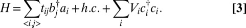 |
Any charge configuration present in the nanopore modifies the on-site potentials in graphene, changing the Hamiltonian (Eq. 3) and thereby the transmission probability (SI Methods). The conductance at the Fermi energy  in the g-QPC can be calculated as
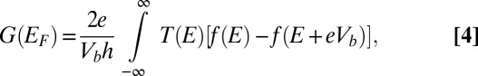 |
where  is the Fermi–Dirac distribution. The carrier concentration
  is controlled by the external gate bias
  , i.e.,
  , where
  is the dielectric capacitance and
  is the threshold voltage for electron or hole conduction in the QPC. Because
  , we use the carrier concentration and the Fermi energy interchangeably, even though the Fermi energy is the relevant parameter. In the following we assume a source–drain bias (
 ) of 5 mV and a system temperature of 300 K. Experimental conductance may be reduced by nonideal boundaries of the QPC. However, the main conclusions pertain to the response of the conductance to changes in the overall geometry and carrier concentration, and they are expected to remain valid if the conductance is significantly reduced, even by an order of magnitude.
Supplementary Material
Acknowledgments
A.G. and J.-P.L. thank Oxford Nanopore Technology for their support. C.S and K.S were supported by National Institutes of Health (NIH) Grants 9P41GM104601 and NIH 5 R01 GMO98243-02. The authors also gratefully acknowledge supercomputer time provided by the Extreme Science and Engineering Discovery Environment (XSEDE) MCA93S028. C.S acknowledges support as a Beckman Graduate Fellow.
Footnotes
The authors declare no conflict of interest.
*This Direct Submission article had a prearranged editor.
This article contains supporting information online at www.pnas.org/lookup/suppl/doi:10.1073/pnas.1308885110/-/DCSupplemental.
References
- 1.Branton D, et al. The potential and challenges of nanopore sequencing. Nat Biotechnol. 2008;26(10):1146–1153. doi: 10.1038/nbt.1495. [DOI] [PMC free article] [PubMed] [Google Scholar]
- 2.Schloss JA. How to get genomes at one ten-thousandth the cost. Nat Biotechnol. 2008;26(10):1113–1115. doi: 10.1038/nbt1008-1113. [DOI] [PubMed] [Google Scholar]
- 3.Schadt EE, Turner S, Kasarskis A. A window into third-generation sequencing. Hum Mol Genet. 2010;19(R2):R227–R240. doi: 10.1093/hmg/ddq416. [DOI] [PubMed] [Google Scholar]
- 4.Derrington IM, et al. Nanopore DNA sequencing with MspA. Proc Natl Acad Sci USA. 2010;107(37):16060–16065. doi: 10.1073/pnas.1001831107. [DOI] [PMC free article] [PubMed] [Google Scholar]
- 5.Li J, Gershow M, Stein D, Brandin E, Golovchenko JA. DNA molecules and configurations in a solid-state nanopore microscope. Nat Mater. 2003;2(9):611–615. doi: 10.1038/nmat965. [DOI] [PubMed] [Google Scholar]
- 6.Storm AJ, Chen JH, Ling XS, Zandbergen HW, Dekker C. Fabrication of solid-state nanopores with single-nanometre precision. Nat Mater. 2003;2(8):537–540. doi: 10.1038/nmat941. [DOI] [PubMed] [Google Scholar]
- 7.Gracheva M, et al. Simulation of the electric response of DNA translocation through a semiconductor nanopore–capacitor. Nanotech. 2006;17(3):622–633. [Google Scholar]
- 8.Gracheva M, Aksimentiev A, Leburton J-P. Electrical signatures of single-stranded DNA with single base mutations in a nanopore capacitor. Nanotech. 2006;17(13):3160–3165. [Google Scholar]
- 9.Xie P, Xiong Q, Fang Y, Qing Q, Lieber CM. Local electrical potential detection of DNA by nanowire-nanopore sensors. Nat Nanotechnol. 2012;7(2):119–125. doi: 10.1038/nnano.2011.217. [DOI] [PMC free article] [PubMed] [Google Scholar]
- 10.Dekker C. Solid-state nanopores. Nat Nanotechnol. 2007;2(4):209–215. doi: 10.1038/nnano.2007.27. [DOI] [PubMed] [Google Scholar]
- 11.Ivanov AP, et al. DNA tunneling detector embedded in a nanopore. Nano Lett. 2011;11(1):279–285. doi: 10.1021/nl103873a. [DOI] [PMC free article] [PubMed] [Google Scholar]
- 12.Saha KK, Drndić M, Nikolić BK. DNA base-specific modulation of microampere transverse edge currents through a metallic graphene nanoribbon with a nanopore. Nano Lett. 2012;12(1):50–55. doi: 10.1021/nl202870y. [DOI] [PMC free article] [PubMed] [Google Scholar]
- 13.Sint K, Wang B, Král P. Selective ion passage through functionalized graphene nanopores. J Am Chem Soc. 2008;130(49):16448–16449. doi: 10.1021/ja804409f. [DOI] [PubMed] [Google Scholar]
- 14.Garaj S, et al. Graphene as a subnanometre trans-electrode membrane. Nature. 2010;467(7312):190–193. doi: 10.1038/nature09379. [DOI] [PMC free article] [PubMed] [Google Scholar]
- 15.Merchant CA, et al. DNA translocation through graphene nanopores. Nano Lett. 2010;10(8):2915–2921. doi: 10.1021/nl101046t. [DOI] [PubMed] [Google Scholar]
- 16.Schneider GF, et al. DNA translocation through graphene nanopores. Nano Lett. 2010;10(8):3163–3167. doi: 10.1021/nl102069z. [DOI] [PubMed] [Google Scholar]
- 17.Venkatesan BM, et al. Stacked graphene-Al2O3 nanopore sensors for sensitive detection of DNA and DNA-protein complexes. ACS Nano. 2012;6(1):441–450. doi: 10.1021/nn203769e. [DOI] [PMC free article] [PubMed] [Google Scholar]
- 18.Sathe C, Zou X, Leburton J-P, Schulten K. Computational investigation of DNA detection using graphene nanopores. ACS Nano. 2011;5(11):8842–8851. doi: 10.1021/nn202989w. [DOI] [PMC free article] [PubMed] [Google Scholar]
- 19.Wells DB, Belkin M, Comer J, Aksimentiev A. Assessing graphene nanopores for sequencing DNA. Nano Lett. 2012;12(8):4117–4123. doi: 10.1021/nl301655d. [DOI] [PMC free article] [PubMed] [Google Scholar]
- 20.Nelson T, Zhang B, Prezhdo OV. Detection of nucleic acids with graphene nanopores: Ab initio characterization of a novel sequencing device. Nano Lett. 2010;10(9):3237–3242. doi: 10.1021/nl9035934. [DOI] [PubMed] [Google Scholar]
- 21.Prasongkit J, Grigoriev A, Pathak B, Ahuja R, Scheicher RH. Transverse conductance of DNA nucleotides in a graphene nanogap from first principles. Nano Lett. 2011;11(5):1941–1945. doi: 10.1021/nl200147x. [DOI] [PubMed] [Google Scholar]
- 22.Avdoshenko SM, et al. Dynamic and electronic transport properties of DNA translocation through graphene nanopores. Nano Lett. 2013;13(5):1969–1976. doi: 10.1021/nl304735k. [DOI] [PubMed] [Google Scholar]
- 23.Castro Neto A, Guinea F, Peres N, Novoselov K, Geim A. The electronic properties of graphene. Rev Mod Phys. 2009;81(1):109–162. [Google Scholar]
- 24.Brey L, Fertig H. Electronic states of graphene nanoribbons studied with the Dirac equation. Phys Rev B. 2006;73(23):235411–235415. [Google Scholar]
- 25.Han MY, Özyilmaz B, Zhang Y, Kim P. Energy band-gap engineering of graphene nanoribbons. Phys Rev Lett. 2007;98(20):206805–206808. doi: 10.1103/PhysRevLett.98.206805. [DOI] [PubMed] [Google Scholar]
- 26.Ezawa M. Peculiar width dependence of the electronic properties of carbon nanoribbons. Phys Rev B. 2006;73(4):045432–045439. [Google Scholar]
- 27.Cervantes-Sodi F, Csanyi G, Piscanec S, Ferrari A. Edge-functionalized and substitutionally doped graphene nanoribbons: Electronic and spin properties. Phys Rev B. 2008;77(16):165427–165439. [Google Scholar]
- 28.Furst J, et al. Electronic properties of graphene antidot lattices. New J Phys. 2009;11(9):095020. [Google Scholar]
- 29.Vanevic M, Stojanovic V, Kindermann M. Character of electronic states in graphene antidot lattices: Flat bands and spatial localization. Phys Rev B. 2008;80(4):045410–045417. [Google Scholar]
- 30.Baskin A, Král P. Electronic structures of porous nanocarbons. Sci Rep. 2011;1(36):36. doi: 10.1038/srep00036. [DOI] [PMC free article] [PubMed] [Google Scholar]
- 31.Ritter KA, Lyding JW. The influence of edge structure on the electronic properties of graphene quantum dots and nanoribbons. Nat Mater. 2009;8(3):235–242. doi: 10.1038/nmat2378. [DOI] [PubMed] [Google Scholar]
- 32.Tapasztó L, Dobrik G, Lambin P, Biró LP. Tailoring the atomic structure of graphene nanoribbons by scanning tunnelling microscope lithography. Nat Nanotechnol. 2008;3(7):397–401. doi: 10.1038/nnano.2008.149. [DOI] [PubMed] [Google Scholar]
- 33.Streetman B, Banerjee S. Solid State Electronic Devices. Upper Saddle River, NJ: Prentice Hall; 2005. [Google Scholar]
- 34.Banerjee S, et al. Electrochemistry at the edge of a single graphene layer in a nanopore. ACS Nano. 2013;7(1):834–843. doi: 10.1021/nn305400n. [DOI] [PMC free article] [PubMed] [Google Scholar]
- 35.Gracheva ME, Melnikov DV, Leburton J-P. Multilayered semiconductor membranes for nanopore ionic conductance modulation. ACS Nano. 2008;2(11):2349–2355. doi: 10.1021/nn8004679. [DOI] [PubMed] [Google Scholar]
- 36.Luan B, et al. Base-by-base ratcheting of single stranded DNA through a solid-state nanopore. Phys Rev Lett. 2010;104(23):238103–239106. doi: 10.1103/PhysRevLett.104.238103. [DOI] [PMC free article] [PubMed] [Google Scholar]
- 37.Melnikov DV, Leburton J-P, Gracheva ME. Slowing down and stretching DNA with an electrically tunable nanopore in a p-n semiconductor membrane. Nanotechnology. 2012;23(25):255501–255506. doi: 10.1088/0957-4484/23/25/255501. [DOI] [PubMed] [Google Scholar]
Associated Data
This section collects any data citations, data availability statements, or supplementary materials included in this article.