Abstract
The template-stripping method can yield smooth patterned films without surface contamination. However, the process is typically limited to coinage metals such as silver and gold because other materials cannot be readily stripped from silicon templates due to strong adhesion. Herein, we report a more general template-stripping method that is applicable to a larger variety of materials, including refractory metals, semiconductors, and oxides. To address the adhesion issue, we introduce a thin gold layer between the template and the deposited materials. After peeling off the combined film from the template, the gold layer can be selectively removed via wet etching to reveal a smooth patterned structure of the desired material. Further, we demonstrate template-stripped multilayer structures that have potential applications for photovoltaics and solar absorbers. An entire patterned device, which can include a transparent conductor, semiconductor absorber, and back contact, can be fabricated. Since our approach can also produce many copies of the patterned structure with high fidelity by reusing the template, a low-cost and high-throughput process in micro- and nanofabrication is provided that is useful for electronics, plasmonics, and nanophotonics.
Keywords: template stripping, refractory metals, oxides, photovoltaics, thermophotovoltaics
1. Introduction
Numerous patterning techniques have been developed to prepare nanostructured materials.1,2 However, despite significant progress, some applications would still benefit from improved methods. For example, many techniques rely on the patterning of polymers with electron-beam lithography,3,4 block-copolymer lithography,5,6 or nanoimprinting,7,8 or on microcontact printing with self-assembled molecular monolayers.9,10 The polymer or monolayer is then used as a mask, and the pattern is transferred into the actual material with ion etching. Unfortunately, even after the removal of this mask, residual carbon deposits can remain that can be detrimental. Moreover, the etching process, which relies on high-energy ions to remove material, can degrade the mechanical, electronic, or optical properties of the final structure. In particular, ions can roughen the surfaces or be embedded in the material, both of which can increase optical and electronic losses.2,11 Finally, since each individual device is patterned separately, nanometer-scale differences can lead to sample-to-sample variations. Therefore, low-cost, high-throughput nanofabrication methods that avoid these problems are still needed to obtain nanostructured films for photonic and electronic applications.
Recently, template stripping has been explored as a possible route.11−15 This process deposits a thin film of a coinage metal, such as silver or gold, on a prepatterned silicon substrate. Since these metals can wet the native oxide on the Si, but adhere poorly, the film can be peeled off, revealing a smooth inverted replica of the original patterned template. This approach is not only simple but can exploit several key advantages. First, the sophisticated patterning techniques developed for Si can be utilized to form the template. Second, after removal of the patterned metal film, the template can be reused many times,11 resulting in a low-cost, high-throughput process. Third, because the metal is not directly patterned (e.g., via ion etching with a polymer mask), contamination and degradation can be completely avoided.
In the field of plasmonics, these advantages can be important because the pattern is used to manipulate electromagnetic waves known as surface plasmon polaritons.16 Template stripping can provide extremely smooth patterned films of pure metals with low loss, leading to better performance.11 In particular, surface roughness that can scatter surface plasmon polaritons is greatly reduced.15,17 Silver and gold are also among the best available materials for many plasmonic applications. Consequently, the restriction of template stripping to such metals is typically not an issue.
However, in other areas, this restriction can be problematic. For example, in photovoltaics, nanostructured films have been explored to enhance light absorption through reflecting, channeling, or concentrating sunlight.18−20 To obtain practical devices, the technique used to introduce the nanostructure must be inexpensive and able to handle large areas. Template stripping could potentially provide a solution, but the use of Ag or Au would increase cost. Other materials, such as Al or metal oxides, could avoid this problem. However, since these materials adhere to a Si substrate, structured films cannot be directly obtained from them via template stripping.
Another example is in thermophotovoltaic devices, where nanostructured films are used to absorb energy from a hot object, such as the sun, and then re-radiate thermal emission that can be converted into electricity by a photocell.21−25 The goal of the film is to convert the broadband emission from the hot object into a narrower spectrum that is better matched to the photocell. Since the nanostructured film must sustain elevated temperatures (typically above 1000 °C), it must be fabricated from a refractory material (e.g., tungsten). Patterning of such materials through conventional methods can present challenges, as discussed further below. Template stripping could again potentially provide a solution. However, due to adhesion of refractory materials to Si substrates, template stripping with such materials has not yet been demonstrated.
Herein, we present a simple scheme to expand template stripping beyond the coinage metals to obtain structures for a broader set of applications. Our approach allows smooth patterning of thin films of refractory metals, semiconductors, and oxides while maintaining the advantages of template stripping discussed above. Consequently, the resulting films can exhibit properties better than those made via conventional patterning techniques. In addition, multilayered stacks of various combinations of materials can be fabricated. Thus, our approach provides a useful tool for low-cost, high-throughput fabrication for various applications.
2. Results and Discussion
While metals such as Ag and Au can be easily peeled off oxide substrates such as mica, glass, and oxidized Si,11,12 refractory metals, semiconductors, and oxides have been regarded as “nonstrippable” due to their strong adhesion to these substrates. To address this problem, we introduce a thin film of a “strippable” metal as a release layer between the substrate and the desired material.13 Although many metals such as Ag, Au, Cu, or Pd could be employed, we use a Au film because its top surface shows very low roughness, leading to smoother surfaces in the final structure.
As shown in Figure 1, the procedure begins by patterning the inverse of the desired structure on the substrate (Figure 1a). A thin Au layer is then deposited (Figure 1b), followed by the deposition of the desired material (Figure 1c). Because Au has a high surface energy, the desired material will be more conformal than if deposited on a polymer. The two layers (Au and desired material) are then peeled off the patterned substrate (Figure 1e) using a backing layer. This step utilizes the fact that the adhesion between the Au and the native oxide on the Si wafer is lower than the adhesion between the Au and the desired material. This is the case for all the examples shown below. For the backing layer, we have previously used a flexible adhesive polymer (like epoxy or polydimethylsiloxane).11 For high temperature applications, where the final structure should not contain any organic materials, the backing layer can instead be made from an electrodeposited metal (such as nickel) or a dissolvable material (such as glucose) that can be easily removed to yield a free-standing structure. In any case, a counter-substrate (like a glass or Si wafer) can be attached to the backing layer before stripping if additional structural stability is required. Since the Au release layer adheres poorly to the template, but sticks to the desired material, the two layers can be easily stripped together. Afterwards, the Au can be selectively removed with a wet etchant such that a patterned structure of the desired material is obtained (Figure 1f). The Au can be recycled if desired.
Figure 1.
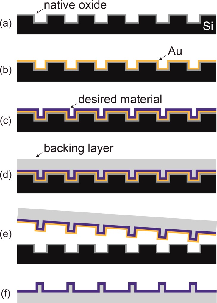
Schematic for the template-stripping approach with a release layer. (a) A silicon (Si) template is patterned by conventional fabrication techniques. (b) A thin gold (Au) layer is deposited on the native oxide of the template. (c) A layer of the desired material is subsequently deposited on the Au. (d) A backing layer is added to the top surface of the deposited films. (e) All of the layers are stripped from the template. (f) The Au is selectively removed by wet etching and can be recycled if necessary.
The surface morphology of the final structure is largely determined by the top surface of the Au release layer. Although very thin Au films can be extremely smooth, if the Au is too thin, it may not completely cover the template and the desired material may not strip off. To avoid this, we first determined the optimal thickness of the Au layer (∼20 nm). Figure 2a shows the surface morphology of the top surface of such a Au film. The root-mean-square (RMS) roughness of this surface was quantified with atomic force microscopy (AFM). The Au has a slightly larger roughness, 0.39 nm, than the original Si substrate, 0.16 nm (see Figure S1 in the Supporting Information).
Figure 2.
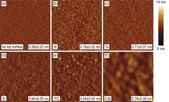
AFM images of flat surfaces for determining surface roughness. (a) Top surface of a 20-nm-thick gold (Au) film. Template-stripped (b) tungsten (W), (c) tantalum (Ta), (d) silicon (Si), (e) indium tin oxide (ITO), and (f) cadmium sulfide (CdS) surfaces. Each image includes the extracted RMS roughness from the 2.5 × 2.5 μm2 scanned area.
The effectiveness of such a Au release layer was tested by fabricating flat films of various materials via template stripping. W, Ta, Si, indium tin oxide (ITO), or cadmium sulfide (CdS) was deposited on the Au via sputtering or chemical bath deposition26,27 (see Experimental Section). To remove the Au after template stripping, a wet etchant containing potassium iodide and iodine was typically used. However, since CdS is also attacked by this etchant, a potassium hydroxide (KOH) and potassium cyanide solution was utilized in this case.28 Figure 2 shows the surface morphology of the flat template-stripped films. All materials exhibit smooth surfaces with an RMS roughness below 0.8 nm. This level of roughness is difficult to achieve in these materials with conventional deposition approaches. For example, under our deposition conditions, the roughness of the top surfaces of our W, Ta, and ITO films were ∼1.8, ∼1.0, and ∼3.1 nm, respectively. For electrodeposited CdS, the roughness is typically well above 10 nm.29
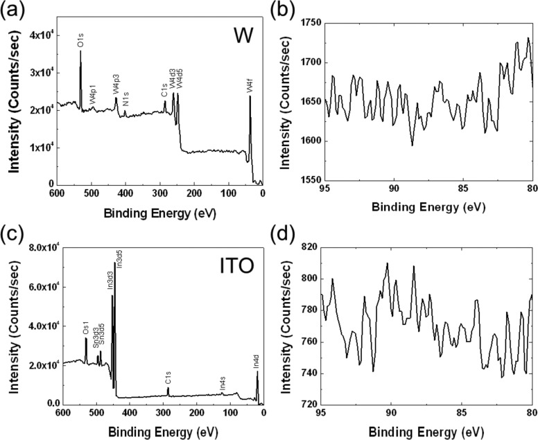
As already mentioned, one advantage of template stripping is that it allows surface contamination to be avoided. To determine if any impurities were present on these template-stripped films, they were characterized with X-ray photoelectron spectroscopy (XPS). In particular, we looked for residual Au left after removal of the release layer. Figure 3 exhibits the XPS spectra for the template-stripped films of W and ITO. As shown in the wide-scan survey spectra (Figure 3a and c), only the expected elements and background species (C, O, and N) are observed; Au was not detected. To confirm this result, high-resolution spectra were collected between 80 and 95 eV where the Au 4f peaks exist.30 No Au peaks were observed (Figure 3b and d). This suggests that the Au release layer was completely removed via the etching process. Similarly, Figure S2 in the Supporting Information shows that Au peaks were also absent in the XPS spectra for template-stripped films of Ta, Si, and CdS. Consequently, the Au content in the template-stripped films of these materials is below the sensitivity of the XPS, 0.1 atom %.
Figure 3.
XPS spectra for template-stripped surfaces of tungsten (W) and indium tin oxide (ITO) films. A wide-scan survey spectrum of the template-stripped (a) W and (c) ITO films. Each image contains the peak annotation. A high-resolution spectrum of the template-stripped (b) W and (d) ITO films in the region of the Au 4f peaks. Au peaks were not observed.
However, we note that for some materials the absence of residual Au depended on the thermal history of the film. The above XPS results were obtained by using ultraviolet-curable epoxy as the backing layer for stripping. XPS was also performed on samples that were obtained from thermally cured epoxy. In that case, Au was still not detected on W and ITO films. However, XPS spectra revealed Au 4f peaks on Ta, Si, and CdS films.
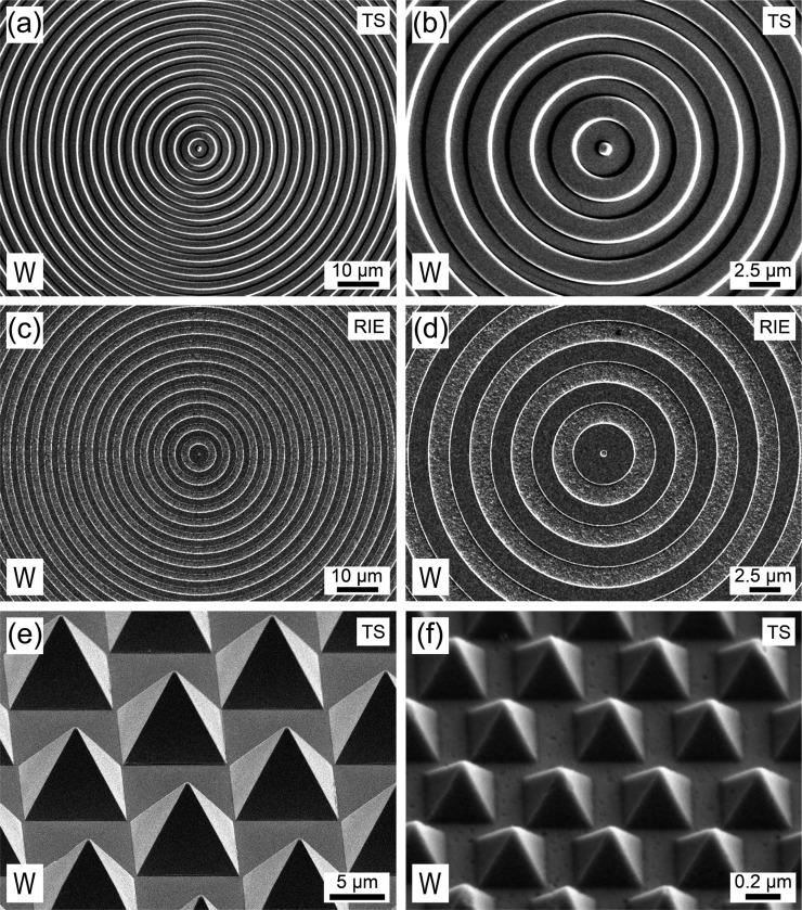
So far we have presented results only for flat films. The same fabrication strategy can be exploited to obtain patterned structures. For example, Figure 4a and b demonstrates a W bull’s eye pattern obtained with this approach. Conventionally, such metal structures would be patterned with reactive-ion etching (RIE), ion milling, or focused-ion-beam (FIB) milling. However, this typically leads to large surface roughness due to the polycrystallinity of the metal. Namely, grains that are oriented in different directions etch at different rates.31,32 Indeed, as shown in Figure 4c and d, a W bull’s eye structure fabricated by RIE exhibits very rough surfaces, especially in the etched grooves. In comparison, the template-stripped structure has smooth surfaces (Figure 4a and b), similar to those previously demonstrated for Ag and Au.11
Figure 4.
Scanning electron micrographs of tungsten (W) structures. (a, b) Bull’s eye pattern prepared via template stripping (TS). (c, d) Bull’s eye pattern made via conventional reactive-ion etching (RIE) for comparison. Both bull’s eye structures have a groove periodicity of 3.5 μm and a groove depth of ∼200 nm. (e) Micro- and (f) nano-scale pyramid arrays prepared by TS. The pyramids have a base length of ∼9 μm and 350 nm, respectively.
This is quantified in Figure 5, which compares the surface morphology of the W bull’s eye structures obtained via RIE with those from template stripping. The RIE sample was obtained by first depositing a W film on a flat silicon substrate via sputtering. Before patterning, the W film had a nominal RMS roughness of about 2 nm on its exposed surface. The pattern was then created by etching this surface with RIE. As this etching proceeds, the surface roughness of the patterned area increases as shown in Figure 5a and b. The final RMS roughness in the 200-nm-deep grooves is about 10 nm. This increase cannot be avoided due to the polycrystallinity of the metal.
Figure 5.
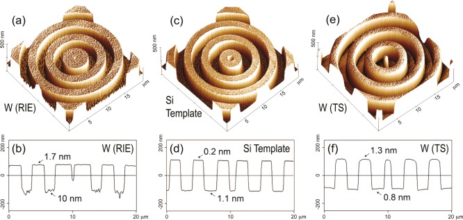
Surface morphology comparison. Three-dimensional AFM images of (a) a tungsten (W) bull’s eye pattern obtained from direct RIE of a W film, (c) a silicon (Si) bull’s eye pattern obtained from direct RIE of a Si wafer, and (e) a W bull’s eye pattern obtained via template stripping from the Si template. (b, d, f) Cross-sectional profile of each structure with the extracted RMS roughness at the top or bottom of the grooves.
However, a single-crystalline substrate like a Si wafer exhibits much more uniform etching, leading to smoothly patterned surfaces.32 Figure 5c and d shows the same bull’s eye pattern in Si obtained via RIE. The RMS roughness at the bottom of the grooves is 10× smaller than that for those directly patterned in the W. Consequently, when this Si is used as a template for W deposition, a template-stripped W bull’s eye that is much smoother is fabricated (Figure 5e, f and Figure S3 in the Supporting Information). The RMS roughness in the grooves and on the top flats was only 0.8 and 1.3 nm, respectively. This implies that the template-stripped structures should exhibit lower optical and electronic losses. If such refractory structures are used for thermophotovoltaic applications, this can lead to better performance.33
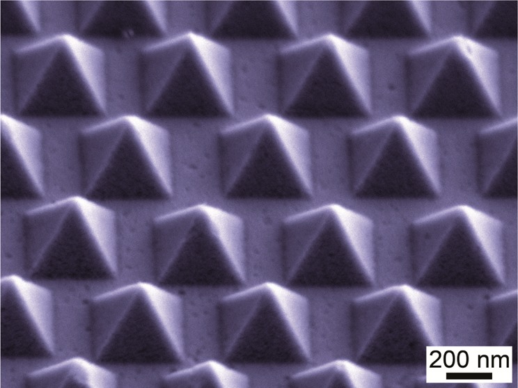
In addition to bull’s eye patterns, arrays of W pyramids were fabricated via template stripping. Such structures have been discussed for their potential application as omnidirectional solar absorbers.34 To prepare suitable templates, we utilized anisotropic etching of Si(100) wafers with KOH.35 Using photolithography or nanosphere lithography, arrays of micro- or nano-scale holes were formed in a Cr layer on the Si substrate, respectively.11,13 These holes were used as the mask for the anisotropic etch, which induced pyramidal etch pits in the Si. The deposition of Au and W layers, template stripping, and wet etching then followed. Figure 4e and f shows the smooth tapered W micro- and nanopyramids obtained. As predicted by previous theoretical calculations,34 the W nanopyramid arrays exhibit much higher absorptivity for visible wavelengths compared to a flat W film (see Figure S4 in the Supporting Information). The taper of the nanopyramids reduces the impedance mismatch for incoming light at the W-air interface, which leads to lower reflectivity and higher absorptivity.
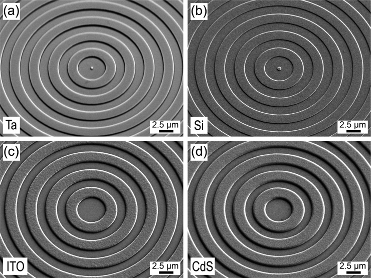
In addition to W, a large variety of materials can be patterned with this template-stripping approach. In the field of micro- and nanofabrication, dry etching is typically used to pattern materials such as refractory metals and oxides, which have a high melting point and stiff elastic modulus. However, the etching process can be affected by many factors, including the mechanical and chemical properties of the material; its crystalline structure, grain orientation, and surface purity; and even the history of the etching chamber. Thus, it is difficult to control patterns on the nanometer scale. In contrast, since our template-stripping method utilizes etching of silicon, which is extremely well developed, accurate control of the same pattern is possible for many materials. Figure 6 shows bull’s eye structures made from Ta, Si, ITO, and CdS via template stripping. All of these structures were prepared with exactly the same groove periodicity (3.5 μm). The groove depth was adjusted from 150 to 300 nm via fine-tuning of the template. Precisely patterned structures with smooth surfaces made from such semiconductors and oxides can be highly useful in the fabrication of various devices including structured semiconductor solar cells18 and plasmonic devices of transparent conducting oxides.36
Figure 6.
Scanning electron micrographs of bull’s eye patterns of (a) tantalum (Ta), (b) silicon (Si), (c) indium tin oxide (ITO), and (d) cadmium sulfide (CdS). The structures all have a 3.5 μm groove periodicity with groove depths of (a) ∼200, (b) ∼150, (c) ∼300, and (d) ∼270 nm. The tops of the ridges are rougher in (c) and (d) than in (a) and (b) because the former were stripped from Si templates with deeper grooves. The roughness in the grooves of the Si templates increases with the duration of the RIE. The images were taken with the sample tilted 30° from normal.
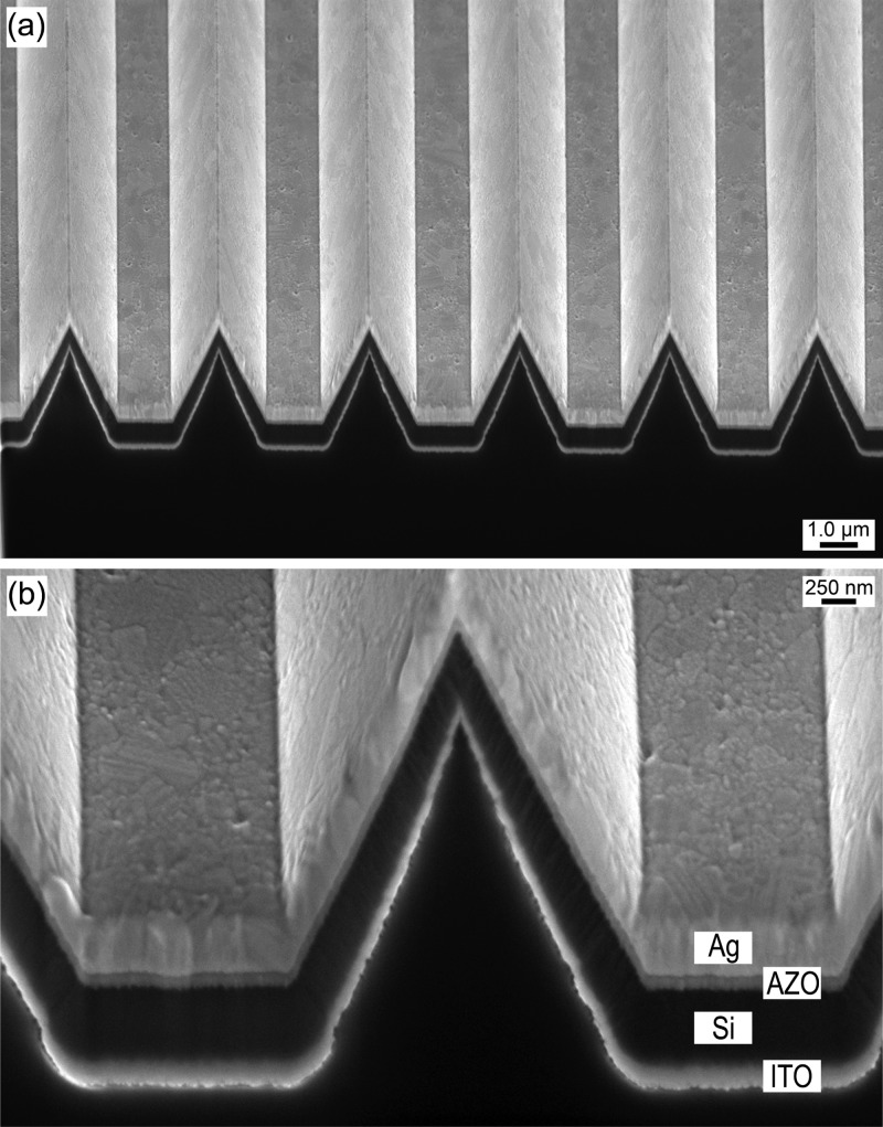
Moreover, patterned multilayer stacks can also be easily created, which can be useful for photovoltaics,19,20 solar absorbers,37 and metamaterials.38,39 For example, Figure 7 shows a wedge structure that contains four layers: Ag, aluminum-doped zinc oxide (AZO), Si, and ITO. As shown in the close-up image (Figure 7b), each layer is continuous and even the bottom layer of ITO still maintains a sharp tip in the wedge. Although the demonstrated structure has a relatively large periodicity of 4 μm compared to previously reported structures,19,20 we have also used template stripping to prepare smaller periodicities. Si templates can be patterned via electron-beam lithography, nanosphere lithography, or FIB milling. While the creation of nanometer-scale patterns with electron-beam lithography or FIB milling over large areas can be slow and costly, template stripping allows this template to be reused many times (>30 times with the upper limit not yet determined), potentially leading to low-cost, high-throughput, and large-scale nanofabrication. For example, the structures in Figures 4f and 7 were both obtained from templates that had been used at least ten times previously.
Figure 7.
Scanning electron micrographs of a multilayered wedge structure made via template stripping. (a) Cross-section obtained by focused-ion-beam milling. (b) Close-up of the cross section showing the four layers of silver (Ag), aluminum-doped zinc oxide (AZO), silicon (Si), and indium tin oxide (ITO) (from top to bottom). These layers have thicknesses of ∼250, ∼65, ∼350, and ∼110 nm, respectively.
3. Conclusions
We have demonstrated that template stripping can provide a general route to various patterned materials beyond the coinage metals. Namely, template stripping can create patterned refractory metals, semiconductors, and oxides. The advantages of template stripping, which were previously demonstrated for Ag, Au, and Cu, are maintained: (i) the surfaces of the resulting films can be smooth without contamination, (ii) a variety of structures can be patterned, and (iii) integrated multilayer architectures can be created. This extends template stripping to high-melting-point solids, such as W, and transparent conductors, such as ITO, both of which are difficult to pattern with conventional methods. Because such materials are becoming increasingly important for applications in photovoltaics, thermophotovoltaics, batteries, and so forth, template stripping offers a simple approach to many optoelectronic, plasmonic, photonic, and electrochemical devices.
4. Experimental Section
Preparation of Silicon Templates
Silicon (100) wafers were used as templates due to their flatness, low cost, and easy processability for patterning and stripping.11 Several different silicon templates were used in this work. The templates for the bull’s eye structures were fabricated using photolithographic techniques. Specifically, positive photoresist (Shipley, Microposit S1805) was spin-coated onto precleaned Si substrates and then exposed under an ultraviolet (UV) lamp through a chrome-on-glass mask with a mask aligner (Karl Suss, MA6). The photoresist on the exposed areas was removed in developing solution (Shipley, Microposit 351 developer). The patterns of the photoresist layer were transferred to the underlying Si substrates by reactive-ion etching (RIE). The RIE process was performed with CF4 and O2 gases, and the depth of the etched parts was controlled by varying the processing time. To obtain the templates with micrometer-scale pyramid structures (micropyramids), Si(100) wafers were coated with a 40-nm-thick chromium layer and then hole arrays were patterned on the chromium layer via photolithographic techniques. The hole arrays act as windows for anisotropic etching of the silicon. Since the (100) planes of the silicon are etched much faster in potassium hydroxide (KOH) solution than the (111) planes, the etching process proceeds until four symmetric (111) planes are exposed. As a result, silicon templates with the four faces of the pyramidal etch pits can be obtained.11,13 After the anisotropic etching process, the chromium layer was etched away with a chromium etchant (Cyantek, CR-7). The templates for the wedge structures were prepared via a similar procedure as that used for the micropyramids. However, instead of hole arrays, gratings were patterned on the chromium layer. Nanosphere lithography13 was used to fabricate the templates with submicrometer-scale pyramid structures (nanopyramids). An aqueous solution containing monodisperse 550-nm-diameter polystyrene spheres (Microparticles GmbH, 10 wt %) was spin-coated onto silicon substrates (800 rpm for 2 min, followed by 1500 rpm for 30 s) to construct a close-packed monolayer. After argon/oxygen plasma treatment to reduce the size of the spheres, the substrates were deposited with a thin chromium layer (∼40 nm) via evaporation. Removing the polystyrene spheres can provide hexagonal hole arrays on the chromium layer, which are then used as a mask for KOH anisotropic etching. All prepared templates were cleaned with piranha solution before deposition.
Deposition of Release Layer and Desired Materials
A thin gold film was introduced as a release layer between the Si templates and the desired materials (refractory metals, semiconductors, and oxides). A 20-nm-thick Au layer was deposited on the patterned templates via thermal evaporation or sputtering. Evaporation was performed at a deposition rate of 0.05 nm/s and a pressure of 1×10⁻⁶ Torr. To avoid detachment of the Au layers during chemical bath deposition, the Au was sputtered for the CdS samples. A DC magnetron at a power of 100 W, a chamber pressure of 6 mTorr Ar, and a source-to-substrate distance of 14 cm were used. Sputtering increased the adhesion of the Au layer to the template, but still allowed template stripping. After evaporation or sputtering of the Au layer, the desired materials were added. W and Ta were deposited with DC magnetron sputtering at a power of 250 W. Si and ITO were deposited with RF magnetron sputtering at a power of 180 and 35 W, respectively. The diameter of all sputtering targets was 50.8 mm. The pressure in the sputtering chamber was maintained at 6 mTorr with Ar during deposition and the source-to-substrate distance was fixed as 14 cm. The sputtering time for each material was controlled to obtain ca. 200-nm-thick layers. For cadmium sulfide (CdS), a chemical bath deposition method was used.27 The CdS layers were grown in an aqueous solution containing 2 mM cadmium chloride, 10 mM thiourea, and 40 mM ammonium chloride at 85 °C. The pH of the solution was adjusted to 9.5 by adding ammonium hydroxide. After 30 min of reaction, about 130-nm-thick CdS films were formed on the substrates.
Template Stripping of the Deposited Films and Removal of the Release Layer
To strip off the deposited films, UV-curable epoxy (Norland Products, NOA 61) was applied to the top surface of the deposited films.11 For most samples, a glass counter substrate was then added and the epoxy layer was cured by exposure to a UV lamp for 1–3 h. The glass, epoxy, and deposited materials were then peeled off the silicon template by using a razor blade. For XPS measurements, some of the samples were stripped using a thermally cured epoxy (Epoxy Technologies, EPO-TEK 377). After adding the epoxy to the top surface of the deposited films, the samples were cured at 120 °C for 5 h.
After stripping, the exposed Au layer of the stripped films was removed with a Au etchant containing potassium iodide and iodine (Transene, GE-6). In most cases, the etchant was very effective at selectively etching away the Au layer without damaging the underlying desired material (such as W, Ta, Si, and ITO). However, CdS was attacked by the Au etchant. Thus, a different etchant was employed in this case. Using an aqueous solution containing 1 M KOH and 0.1 M potassium cyanide with oxygen purging, the gold layer could be selectively etched off without damaging the CdS films.28
Fabrication of Bull’s Eye Structures via Direct Etching
Figures 4 and 5 compare W bull’s eye structures prepared by conventional etching (Figure 4c and d) with those obtained with template stripping (Figure 4a and b). To fabricate the conventional bull’s eye structures, 500-nm-thick W films were first deposited on flat Si substrates by sputtering. Photoresist was coated on the W films and then exposed under a UV lamp through a mask for bull’s eye patterns. The patterns of the photoresist were transferred into the underlying W films by RIE. The RIE process was performed with SF6 (50 sccm) and Ar (10 sccm) gases, a power of 50 W, a pressure of 50 mTorr, and an etch rate of ∼1.5 nm/s. The depth of the grooves was adjusted by the etching time.
Fabrication of Multilayer Structures via Template Stripping
Multilayer structures composed of metal, semiconductor, and oxide layers were also fabricated by the template-stripping method, as demonstrated in Figure 7. Silicon templates for wedge structures were prepared via KOH anisotropic etching, as discussed above. Then 250 nm of Ag, 65 nm of aluminum-doped zinc oxide, 350 nm of Si, and 110 nm of ITO were sequentially deposited on the template by sputtering. Wedge structures containing these four layers were stripped with the epoxy backing layer, revealing smooth Ag surfaces. To observe the cross sections of the multilayer structures shown in Figure 7, the structures were cut by focused-ion-beam milling with 30 kV as the acceleration voltage and 150 pA as the ion-beam current.
Characterization of Surface Morphology
An atomic force microscope (AFM, Agilent 5500) was utilized to characterize the surface morphology of the prepared structures. All AFM images were obtained by using tapping mode, and the root-mean-square (RMS) roughness of the stripped surfaces was determined with 2.5 × 2.5 μm2 scans.
Characterization of Impurities on Template-Stripped Surfaces
The impurities on the template-stripped surfaces were characterized with X-ray photoelectron spectroscopy (XPS, PHI 5000 VersaProbe). The X-ray source was Al Kα (1486.6 eV), and 25 W (15 kV) was applied to the source. The photoelectrons were detected at an angle of 45° from normal under ultrahigh vacuum (base pressure of 6.7 × 10⁻⁸ Pa). The analyzer pass energy for the wide scan and the high-resolution scan was 117.40 and 23.50 eV, respectively.
Optical Characterization of Nanopyramid Arrays
Optical characterization of the W nanopyramid arrays was performed with a tungsten-halogen lamp, liquid-nitrogen-cooled CCD photodetector (Princeton Instruments), and an inverted optical microscope (Nikon TE 200). A W nanopyramid film was illuminated by the lamp, and the reflected light was collected using a high-numerical-aperture (NA) objective lens (100×, NA = 0.9). The reflected image of the nanopyramid arrays was then formed on the detector and analyzed spectroscopically. A flat single-crystalline Ag film32 with RMS surface roughness of ∼1 nm was employed as a reference to obtain the absolute reflectivity of the sample, at each wavelength. The reflectivity of this Ag reference sample was independently determined via ellipsometry. Absorptivity was estimated from 1 – R, where R is the reflectivity. Thus, any light scattered at high angles was neglected. A flat 350-nm-thick W film with RMS surface roughness of ∼1 nm was prepared by DC magnetron sputtering, and the absorptivity was compared with the W nanopyramid film.
Acknowledgments
This project was supported by the 7th Framework Programme of the European Commission under the HRC Power project. Additional support was provided by the U.S. Department of Energy, Office of Basic Energy Sciences, Division of Materials Sciences and Engineering under Award DE-FG02-06ER46438. The authors used resources at the University of Minnesota, including the Nanofabrication Center, which receives partial support from the U.S. National Science Foundation (NSF) through the National Nanotechnology Infrastructure Network, and the Characterization Facility, which has received capital equipment funding through the NSF Materials Research Science and Engineering Center program. S.-H.O. acknowledges support from the Office of Naval Research Young Investigator Award (N00014-11-1-0645).
Supporting Information Available
Figures S1–S4, in detail: Figure S1, AFM images of a silicon wafer and a template-stripped Au film; Figure S2, XPS spectra for the template-stripped surfaces of Ta, Si, and CdS films; Figure S3, AFM images of template-stripped W bull’s eye structures; Figure S4, absorption spectra for W nanopyramid films fabricated by template stripping and flat W films. This material is available free of charge via the Internet at http://pubs.acs.org.
Author Present Address
⊥ P.N.: Department of Chemical and Biological Engineering, University of Colorado, Boulder, CO 80303, USA.
Author Present Address
# N.C.L.: Physics Department, Bethel University, Saint Paul, MN 55112, USA.
The authors declare no competing financial interest.
Supplementary Material
References
- Gates B. D.; Xu Q.; Stewart M.; Ryan D.; Willson C. G.; Whitesides G. M. Chem. Rev. 2005, 105, 1171–1196. [DOI] [PubMed] [Google Scholar]
- Lindquist N. C.; Nagpal P.; McPeak K. M.; Norris D. J.; Oh S.-H. Rep. Prog. Phys. 2012, 75, 036501. [DOI] [PMC free article] [PubMed] [Google Scholar]
- Vieu C.; Carcenac F.; Pépin A.; Chen Y.; Mejias M.; Lebib A.; Manin-Ferlazzo L.; Couraud L.; Launois H. Appl. Surf. Sci. 2000, 164, 111–117. [Google Scholar]
- Joo J.; Chow B. Y.; Jacobson J. M. Nano Lett. 2006, 6, 2021–2025. [DOI] [PubMed] [Google Scholar]
- Park M.; Harrison C.; Chaikin P. M.; Register R. A.; Adamson D. H. Science 1997, 276, 1401–1404. [Google Scholar]
- Jeong S.-J.; Xia G.; Kim B. H.; Shin D. O.; Kwon S.-H.; Kang S.-W.; Kim S. O. Adv. Mater. 2008, 20, 1898–1904. [Google Scholar]
- Kim E.; Xia Y. N.; Whitesides G. M. Nature 1995, 376, 581–584. [Google Scholar]
- Chou S. Y.; Krauss P. R.; Renstrom P. J. Science 1996, 272, 85–87. [Google Scholar]
- Kumar A.; Whitesides G. M. Appl. Phys. Lett. 1993, 63, 2002–2004. [Google Scholar]
- Geissler M.; Schmid H.; Bietsch A.; Michel B.; Delamarche E. Langmuir 2002, 18, 2374–2377. [Google Scholar]
- Nagpal P.; Lindquist N. C.; Oh S.-H.; Norris D. J. Science 2009, 325, 594–597. [DOI] [PubMed] [Google Scholar]
- Hegner M.; Wagner P.; Semenza G. Surf. Sci. 1993, 291, 39–46. [Google Scholar]
- Sun C.-H.; Linn N. C.; Jiang P. Chem. Mater. 2007, 19, 4551–4556. [Google Scholar]
- Lindquist N. C.; Johnson T. W.; Norris D. J.; Oh S.-H. Nano Lett. 2011, 11, 3526–3530. [DOI] [PubMed] [Google Scholar]
- Park J. H.; Nagpal P.; Oh S.-H.; Norris D. J. Appl. Phys. Lett. 2012, 100, 081105. [Google Scholar]
- Raether H.Surface Plasmons; Springer-Verlag: Berlin, 1988. [Google Scholar]
- Lindquist N. C.; Nagpal P.; Lesuffleur A.; Norris D. J.; Oh S.-H. Nano Lett. 2010, 10, 1369–1373. [DOI] [PubMed] [Google Scholar]
- Atwater H. A.; Polman A. Nat. Mater. 2010, 9, 205–213. [DOI] [PubMed] [Google Scholar]
- Ferry V. E.; Verschuuren M. A.; Li H. B. T.; Verhagen E.; Walters R. J.; Schropp R. E. I.; Atwater H. A.; Polman A. Opt. Express 2010, 18, A237–A245. [DOI] [PubMed] [Google Scholar]
- Zhu J.; Hsu C.-M.; Yu Z. F.; Fan S. H.; Cui Y. Nano Lett. 2010, 10, 1979–1984. [DOI] [PubMed] [Google Scholar]
- Bauer T.Thermophotovoltaics: Basic Principles and Critical Aspects of System Design; Springer-Verlag: Berlin, 2011. [Google Scholar]
- Heinzel A.; Boerner V.; Gombert A.; Bläsi B.; Wittwer V.; Luther J. J. Mod. Opt. 2000, 47, 2399–2419. [Google Scholar]
- Lin S. Y.; Moreno J.; Fleming J. G. Appl. Phys. Lett. 2003, 83, 380–382. [Google Scholar]
- Nagpal P.; Han S. E.; Stein A.; Norris D. J. Nano Lett. 2008, 8, 3238–3243. [DOI] [PubMed] [Google Scholar]
- Liu X.; Tyler T.; Starr T.; Starr A. F.; Jokerst N. M.; Padilla W. J. Phys. Rev. Lett. 2011, 107, 045901. [DOI] [PubMed] [Google Scholar]
- Ortega-Borges R.; Lincot D. J. Electrochem. Soc. 1993, 140, 3464–3473. [Google Scholar]
- Dhere N. G.; Waterhouse D. L.; Sundaram K. B.; Melendez O.; Parikh N. R.; Patnaik B. J. Mater. Sci.: Mater. Electron. 1995, 6, 52–59. [Google Scholar]
- Kumar A.; Biebuyck H. A.; Abbott N. L.; Whitesides G. M. J. Am. Chem. Soc. 1992, 114, 9188–9189. [Google Scholar]
- Nel J. M.; Gaigher H. L.; Auret F. D. Thin Solid Films 2003, 436, 186. [Google Scholar]
- Christ B. V.Handbook of Monochromatic XPS Spectra, Vol 1, The Elements and Native Oxides; XPS International Inc.: Mountain View, CA, 1999. [Google Scholar]
- Volkert C. A.; Minor A. M. MRS Bull. 2007, 32, 389–395. [Google Scholar]
- Park J. H.; Ambwani P.; Manno M.; Lindquist N. C.; Nagpal P.; Oh S.-H.; Leighton C.; Norris D. J. Adv. Mater. 2012, 24, 3988–3992. [DOI] [PubMed] [Google Scholar]
- Han S. E.; Norris D. J. Opt. Express 2010, 18, 4829–4837. [DOI] [PubMed] [Google Scholar]
- Rephaeli E.; Fan S. Appl. Phys. Lett. 2008, 92, 211107. [Google Scholar]
- Campbell S. A.The Science and Engineering of Microelectronic Fabrication; Oxford University Press: New York, 2001. [Google Scholar]
- West P. R.; Ishii S.; Naik G. V.; Emani N. K.; Shalaev V. M.; Boltasseva A. Laser Photonics Rev. 2010, 4, 795–808. [Google Scholar]
- Sergeant N. P.; Agrawal M.; Peumans P. Opt. Express 2010, 18, 5525–5540. [DOI] [PubMed] [Google Scholar]
- Smith D. R.; Pendry J. B.; Wiltshire M. C. K. Science 2004, 305, 788–792. [DOI] [PubMed] [Google Scholar]
- Valentine J.; Zhang S.; Zentgraf T.; Ulin-Avila E.; Genov D. A.; Bartal G.; Zhang X. Nature 2008, 455, 376–379. [DOI] [PubMed] [Google Scholar]
Associated Data
This section collects any data citations, data availability statements, or supplementary materials included in this article.


