Abstract
In this paper we present a fixed window level crossing sampling analog to digital convertor for bio-potential recording sensors. This is the first proposed and fully implemented fixed window level crossing ADC without local DACs and clocks. The circuit is designed to reduce data size, power, and silicon area in future wireless neurophysiological sensor systems. We built a testing system to measure bio-potential signals and used it to evaluate the performance of the circuit. The bio-potential amplifier offers a gain of 53 dB within a bandwidth of 200 Hz-20 kHz. The input-referred rms noise is 2.8 µV. In the asynchronous level crossing ADC, the minimum delta resolution is 4 mV. The input signal frequency of the ADC is up to 5 kHz. The system was fabricated using the AMI 0.5 µm CMOS process. The chip size is 1.5 mm by 1.5 mm. The power consumption of the 4-channel system from a 3.3 V supply is 118.8 µW in the static state and 501.6 µW with a 240 kS/s sampling rate. The conversion efficiency is 1.6 nJ/conversion.
Index Terms: Analog to digital conversion (ADC), asynchronous delta modulation (ADM), bio-potential recording applications, clock-less operation, continuous time level crossing sampling, fixed window method, large-scale sensor array
I. Introduction
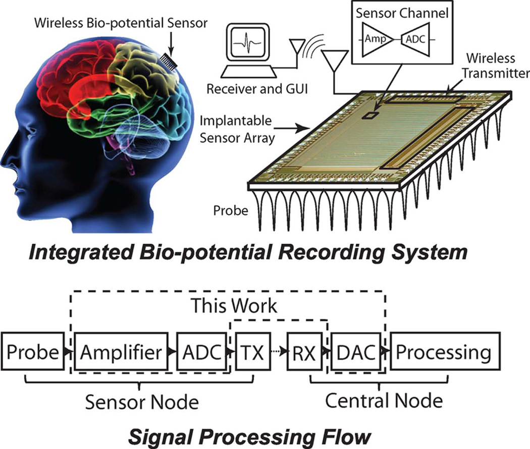
IN RECENT years, scientists in neurophysiology desire large-scale sensor arrays with high speed and low power to record in vivo bio-potential signals [1]. The goal is to monitor the neural activity of freely moving animals in real time. In such applications, the sensor array is implanted fully inside [2] or mounted partially outside the animal’s body [3], [4]. In the sensor array, each channel amplifies an analog neural signal and converts it into digital format. Data from individual channels will be organized in a global data packet and transmitted to the receiver wirelessly. At the receiver, the detected digital data is converted back to the analog signal for analysis. Fig. 1 shows a typical bio-potential recording system. The implantable sensor array contains an analog front-end and an analog to digital convertor in each sensor channel, as well as a global wireless transmitter.
Fig. 1.
Implantable bio-potential recording sensor array system. The detected neural signal is amplified and converted to a digital signal by many individual channels and sent by the wireless transmitter (TX). A graphical user interface (GUI) reconstructs the waveform from the receiver (RX), and records the analog signal for every channel.
In such a system, the main challenge is how to handle the increase in data size, when the sensor scales up while the data rate and power consumption are limited by the wireless communication circuitry. For instance, a sensor array with 100 channels will require a wireless transmission link with a data rate over 10 Mbps using less than 10 mW of power [2]. These power and speed constraints are challenging for existing low power wireless devices. This problem can be attributed to traditional synchronous sampling and conversion methods [5]. Most current systems [1]–[4], [6]–[10] use clocked sampling ADCs operating at the fixed Nyquist rate or a higher sampling frequency. However, when recording from multiple neurons, the neural signal is inactive during a large portion of the recording time. During the inactive time of the neuron, constantly sampling the sparse signal and performing a full range analog to digital conversion will waste the resources of the higher significant bits. In order to reduce the data size of the sensor array, on-chip spike sorting and data compression algorithms have been proposed, but those methods increase system power and complexity.
Another challenge of the current design is the power constraint of the ADCs at individual local sensors. A battery-supplied sensor array system requires less than 50 mW total power consumption in order to keep the sensor array working for two weeks. From our experience with a wireless image sensor [11], which is similar to the case of a wireless sensor array, more than 60% of the power of the sensor array will be consumed by the wireless circuit, leaving less than 40% of the power available for the ADCs and amplifiers.
The third consideration is the silicon area of the individual sensor circuit in the large scale sensor array. A local ADC in each channel should be designed with low complexity and small silicon area in order to be implemented in the whole sensor array. It is not applicable to use a global ADC for the whole sensor array because when the number of sensors increases, the required sampling rate of the ADC will be in the 10 million samples per second level, which is too high for the limited power budget.
In order to face the data compression, power and area challenges introduced by the large scale sensor array, efforts have been made to minimize the operation in the local sensors. The variable resolution ADC [8], integration based asynchronous ADC [12]–[15] and level crossing sampling ADC [14]–[24] have been proposed. In this work, we explored the fixed window asynchronous level crossing sampling techniques in order to reduce the power and complexity of the sensor circuit. In the level crossing ADC, sampling is first performed in amplitude domain, then quantization is performed in time domain. As we will demonstrate in the following sections, the asynchronous ADC performs data rate compression better than the clocked ADC for sparse signals. Also in the asynchronous ADC, the level crossing ADC has better dc offset immunity than the integrated-and-fire ADC.
The level crossing sampling ADC was originally proposed in 1966 [25], and was also called asynchronous delta modulation. Theoretical analysis has been made [26]–[33] and some applications related to ultrasound and audio/ECG recording have been investigated at the simulation level [34]–[38]. When the input signal is inactive within the threshold window, no sampling is made and no conversion is performed. So the circuit is working in low power mode. This is also called an Activity-Dependent Power Dissipation System [39]. The level crossing sampling ADC provides data compression, which can assist in tackling the critical challenge in the sensor array. Compared to the clocked sampling systems, the level crossing sampling ADC will reduce the data rate when the signal is sparse. These properties are attractive to most sensor array applications when they are detecting burst-like signals.
In this paper, we propose a new “fixed window” level crossing sampling method by subtracting the input signal. This method removes the local DAC in previously reported references, which used the “floating window” method. Without generating and updating reference voltages, the fixed window method trades simplicity, power and silicon area with resolution, while it still obtains acceptable resolution for the application. This trade-off is important when ADCs are integrated into a large scale sensor array, in which power and silicon area constraints are applied. The main contribution of this paper is to provide a low complexity and low power design of level crossing sampling ADC in the wireless bio-potential sensor array.
The paper is organized as follows. Section II-A gives an overview of level crossing method and a comparison between the fixed window method and the floating window method. Section II-B compares the level crossing sampling ADC to the clocked sampling ADC and describes the system considerations in bio-potential recording applications. Section II-C discusses the difference between the level crossing method and the integrated-and-fire method. Section II-D discusses asynchronous wireless solutions for the level-crossing ADC. Section III presents the circuits and systems design of the fixed window level crossing ADC. Test-bed and measurement results are reported in Sections IV and V, respectively. A summary is given in Section VI.
II. System Considerations
A. Fixed Window Level Crossing ADC
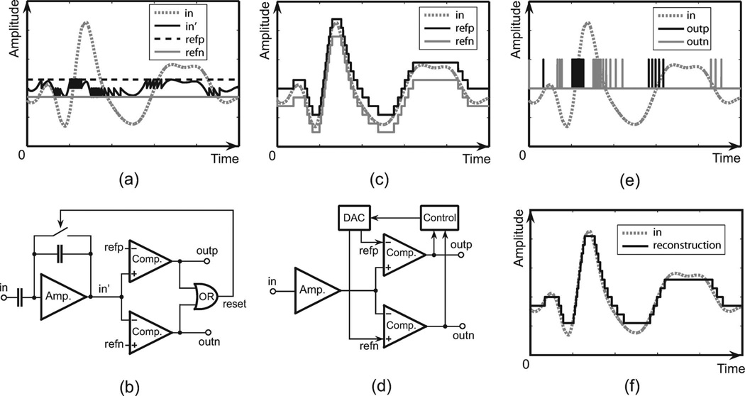
The level crossing ADC converts the analog amplitude of the input signal to an asynchronous digital pulse sequence. The output pulses are generated when the input signal is crossing the threshold window. The number of the output pulses is proportional to the variation rate of the input signal. Existing level crossing sampling ADCs are implemented using the “floating window” method. In this paper, we propose, design and test a new level crossing sampling method using the “fixed window”. As shown in Fig. 2, when the input signal is crossing a certain amplitude level, the fixed window method [Fig. 2(a) and (b)] changes the input signal while the floating window method [Fig. 2(c) and (d)] changes the level threshold. In [39], a floating window circuit is demonstrated. Also in [23], another floating window level crossing ADC is partially integrated on chip. However, in those works, a local DAC with a resistor or capacitor bank in the control unit will cause relatively high power and silicon area in each channel, which is not applicable for integration in a large sensor array. In order to solve the problem, in this paper we present a new structure using the fixed window method with subtraction. The ADC in a local sensor just uses two comparators. No local resistor or capacitor bank is needed or used. It also avoids using a local clock. The subtraction is performed by capacitor feedback and resetting of the analog buffer. The circuits are introduced in Section III-A. Although sampling noise is introduced by resetting the analog buffer, this method could save power and area for the applications of the large sensor array. The output digital pulse sequence and the reconstructed waveform from the fixed window method and the floating window method are identical, and the simulated waveform is shown in Fig. 2(e) and (f).
Fig. 2.
Continuous time level crossing sampling methods, (a)–(b) fixed window method schematic and simulated waveform of this work, (c)–(d) Floating window method schematic and simulated waveform, (e) Level crossing sampling input and output simulated waveform, (f) Simulated reconstructed waveform.
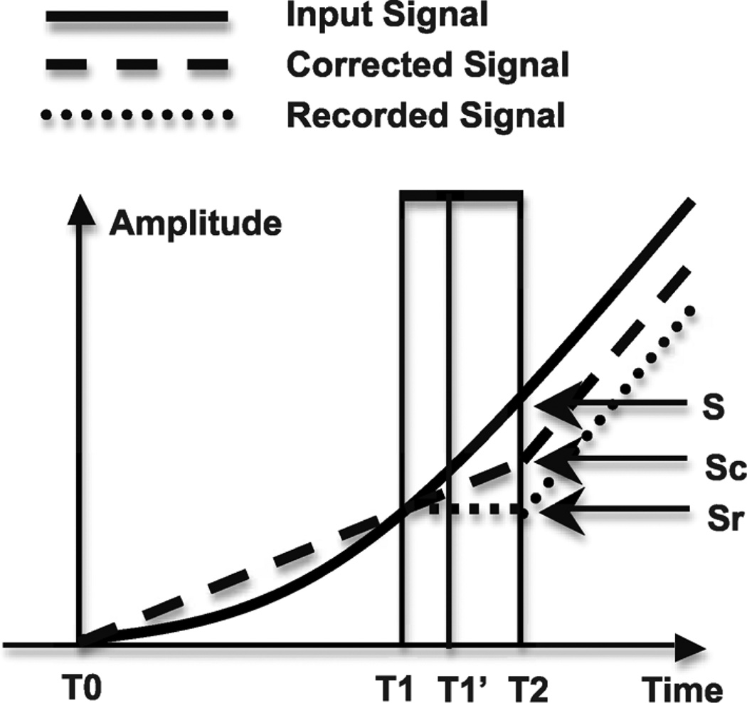
The fixed window method with resetting provides a low complexity implementation in a level-crossing sampling ADC, which makes it possible to integrate ADCs in every channel in the large sensor array while providing data compression. However, resetting the analog input in a continuous time system will cause signal loss during the sampling time, due to the finite response time of the comparators and the switched-capacitor circuits. In [23], the SNR of the floating window level crossing sampling ADC is calculated based on a finite time resolution ratio. However in a fixed window level crossing sampling ADC, another sampling noise is added to the system due to the finite loop delay time of the delta modulator. As illustrated in Fig. 3, the lost signal amplitude is proportional to the output pulse width. The accumulation of the signal loss will cause distortion and dc shift in the recorded signal. That limits the fixed window method from being used in high resolution (>8 bits) applications. However, if the resetting time is much shorter compared to the input signal bandwidth, the resolution of the fixed window method will still be acceptable. The accumulated sampling noise can be modeled as
| (1) |
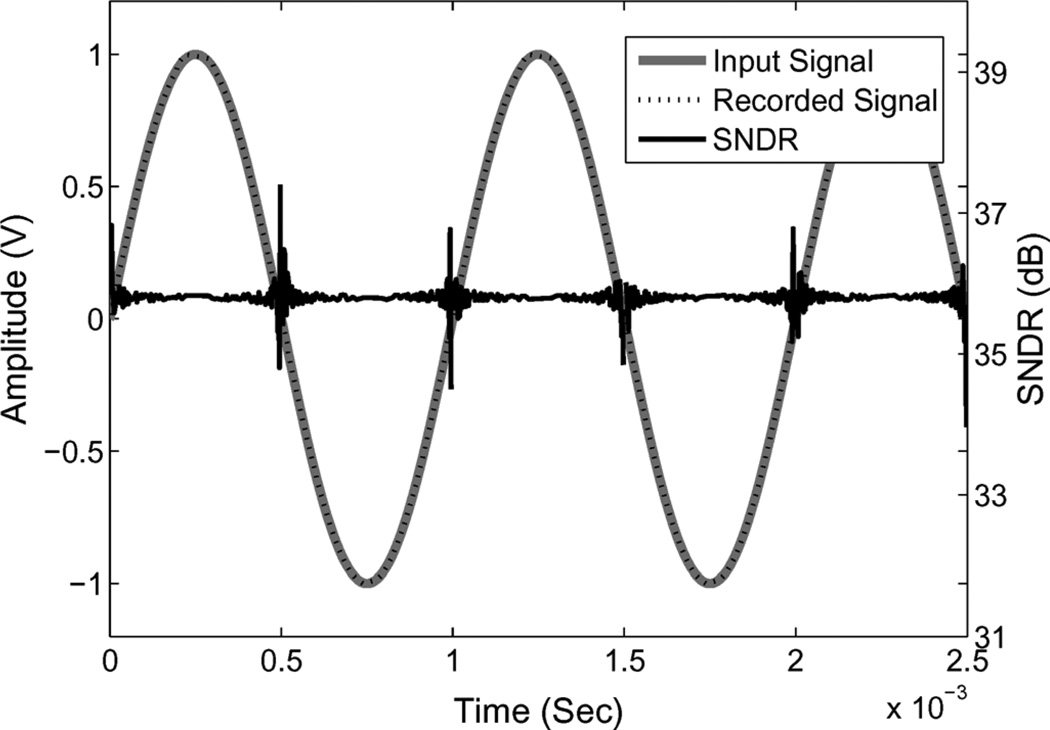
Where E is the amplitude of the accumulated sampling noise, which will add distortion in the reconstructed waveform by reducing its amplitude. A is the signal amplitude. Tloop is the loop delay time from the delta modulator, which includes the reseting time of the buffer and capacitors. The propagation delay of the comparator is Tdelay. Tsignal is the rising time of the spike from peak to peak. The second term represents the root-mean-square (RMS) quantization error in time domain [23]. finput input signal frequency and fclock is the sampling clock frequency for reconstruction. The sampling noise increases with the number of resolution bits. If the loop delay Tloop is 30 ns and the propagation delay of the comparator Tdelay is 6 ns, and the rising time of the spike Tsignal is 300 us, with N = 7, the signal to sampling noise ratio (A/E) will be 37.3 dB, which is below the SNR requirement of a 7 bit ADC (6.02*7+1.76 = 43.9 dB). Therefore, in such a case the maximum resolution of the fixed window level crossing sampling ADC is 6 bits. The pulse width also depends on the common mode voltage of the comparators, process variation and other random noise generated from the comparator. In order to reduce this problem, the positive and negative delta step should be equal and close to virtual ground (1/2 VDD). Equation (2) converted from (1) represents the general signal to noise ratio. Fig. 4 shows the simulated SNDR from the above estimation. The time domain SNDR variation comes from the misalignment of the reconstruction clock with the asynchronous level crossing event.
| (2) |
Fig. 3.
Loop delay induced sampling noise in fixed window level crossing ADC. The previous pulse ends at TO, the current pulse starts at T1’ and finishes at T2. T1 to T1’ is the propagation delay of the comparator. The input signal between T1 and T2 will be lost. The amplitude between S and Sr is the sampling noise. The sampling noise can be partially compensated in the digital domain by estimating the slope of the input signal using extrapolation from the previous pulse, as shown as Sc. The sampling error can be reduced by implementing delta modulator with shorter loop delay.
Fig. 4.
Simulated input signal, recored signal and SNDR of the recorded signal using fixed window method when resolution is 6 bit. The SNDR varies with the time domain sampling noise.
The sampling noise could be partially corrected with digital processing by estimating the slope of the pulse using extrapolation from the previous pulse. The sampling noise can also be reduced by a short loop delay time. The accumulation of sampling noise can cause low frequency shift in the reconstructed signal. In our design we removed the dc component during reconstruction by using a digital filter.
B. Level Crossing ADC for Bio-Potential Signal
In vivo bio-potential recording systems monitor the precise spike shape in order to perform spike sorting and analysis. In the sampling and reconstruction process, when we compare the reconstructed signal and the original signal, the largest error does not usually occur on the sampling points, but rather between the sampling points, especially when we are trying to record the peak of a spike, which is very important in this application. In order to suppress the error under a certain requirement, the sampling and quantization process are correlated: To suppress the error under the quantization noise level for the given resolution, a higher sampling rate must be applied. Sampling at the Nyquist rate, which is double the signal bandwidth, is usually not enough to reliably sample the peak of the spike when we are using zero or first order recovery. A spike signal sequence can be represented by
| (3) |
Here f(t) is the bio-potential signal sequence, the first term on the right hand side represents the background noise waveform, which contains environmental noise and spikes from other neurons surrounding the probe. An (t), ωn and ϕn are the amplitude, angle frequency and phase of the background noise waveform. The second term on the right hand side represents the target bio-potential signal spikes. Here, we simplify a signal spike as a cosine function. i indicates the number of the spike. For a single spike, Ai, ωi and ϕi are the amplitude, angle frequency and phase of the ith spike, respectively. The ith spike started at time tsi and finished at tfi. The measured frequency spectrum of a spike sequence contains frequency component up to several mega hertz, although most of the spike durations are over 0.5 ms.
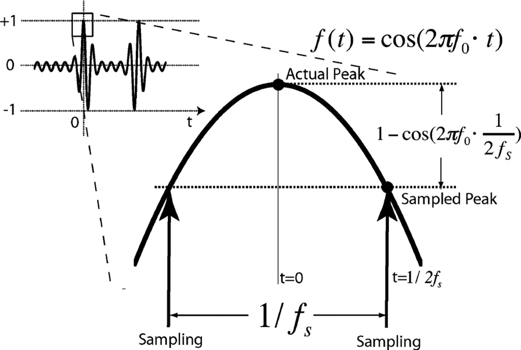
To simplify the analysis, we assume zero order hold reconstruction is applied to both the clocked sampling ADC and the level crossing ADC. When the clocked sampling method is applied, the sampling frequency should be fast enough to meet the requirement of the quantization resolution, especially when we are trying to record the peak of a spike for spike sorting and other analysis. On the other hand, high quantization resolution is meaningless if the sampling rate is not fast enough, as the reconstruction error between the sampling points will exceed the amplitude of the least significant bit (LSB). As shown in Fig. 5, in a N bit resolution clocked system, in order to record the peak of a spike within the error of Err by using zero or first order recovery, we have (4) to represent the maximum Err required for the N bit quantization process. Here the spike is simplified as a cosine wave with frequency of f0, the peak-to-peak amplitude of the spike is normalized from −1 to +1.
| (4) |
Fig. 5.
A simplified spike model to calculate the required sampling rate for certain quantization resolution. The sampling frequency should be fast enough in order to reliably sample the peak of a spike.
We then calculate the required sampling rate fs. In order to guarantee the maximum error Err is less than the resolution LSB of the quantizer, we consider the worst case. In the worst case the sampling point is located symmetrically beside the peak of the spike. Fig. 5 and (5) represent that scenario. Based on (4) and (5), the required sampling rate fs is calculated in (6).
| (5) |
| (6) |
Here, fS is the minimum required sampling rate when the quantization resolution is N bit.
In the bio-potential recording application, if clocked sampling ADCs are used, most of the sampling points will be taken during the non-spike period. They represent the background noise, which is not of interest. Those points will occupy the limited bandwidth resource of the wireless device during wireless data transmission. To solve this problem, we examine the level crossing sampling ADCs and calculate the sampling rate in (7).
| (7) |
Here fLS and f0 are the level crossing sampling frequency and the simplified spike signal frequency, respectively. N is the total number of resolution bits. Because both the rising edge and falling edge of the signal will be sampled in one period, fLS is 2N+1 times the f0. For a cosine waveform with a frequency of f0 and rail-to-rail amplitude, by comparing (6) and (7), we conclude that in order to obtain the same amplitude resolution N, the level crossing sampling method will take more sampling points than the clocked sampling method. However, in bio-potential recording applications, the final data size of the level crossing method may be smaller than the clocked sampling method, especially when the resolution is low. This happens first because at every sampling point, the clocked sampling method needs N bits to represent the information, while the level crossing method only needs the polarity to characterize the sampling point (i.e., 2 bits for every sampling point to represent a positive or negative delta step change). Second, the number of sampling points from the level crossing sampling method will be remarkably reduced if the target signal has a low activity ratio.
The activity ratio is a statistical signal property. It is defined by using the level crossing sampling method. For a certain amplitude level Li, where i is the number of the threshold level, fLi is the frequency of the signal crossing the level Li. If the target signal frequency is f0, we define the signal activity ratio Ract by (8).
| (8) |
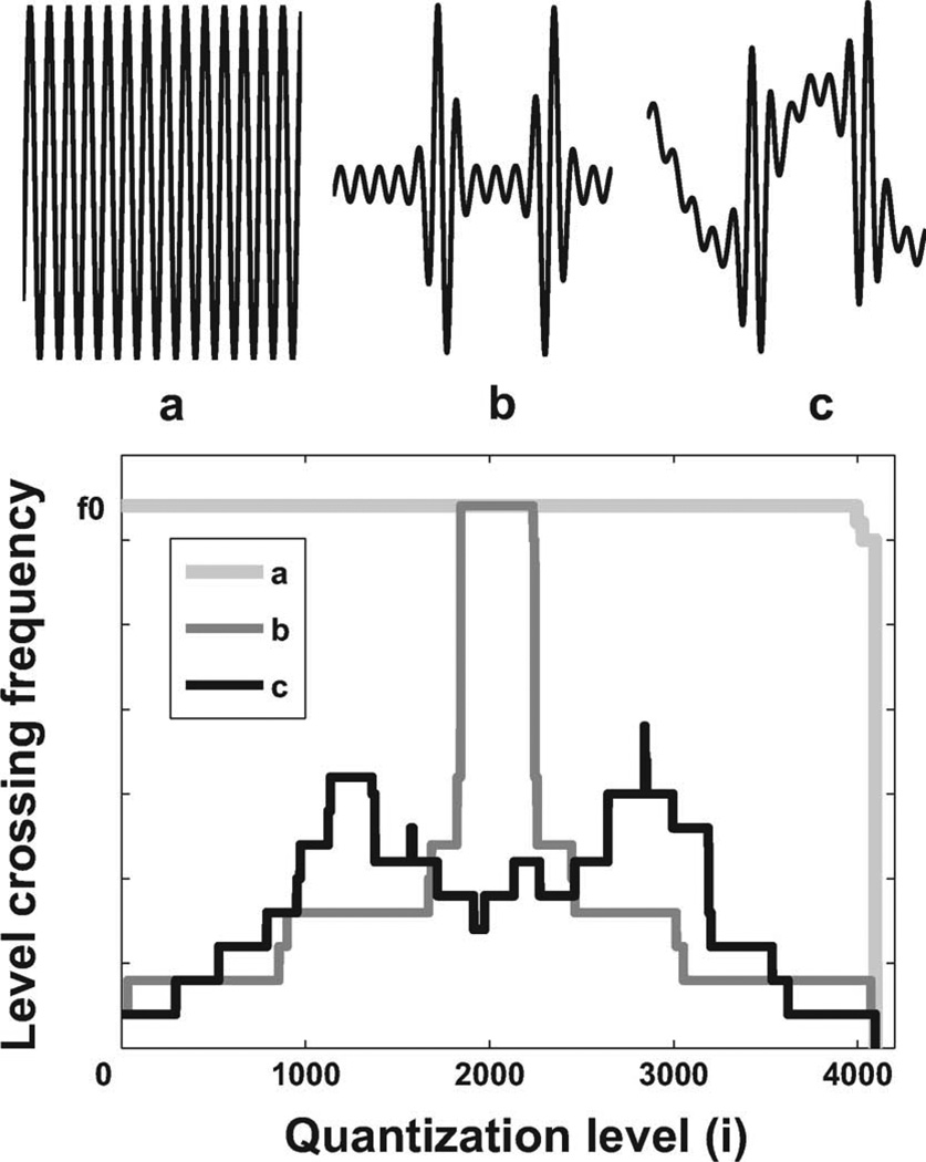
fLi means the frequency of the signal crossing the ith amplitude level. The numerator of the right-hand-side represents the total level-crossing frequency of the signal for all levels. The denominator of the right-hand-side is the maximum level crossing frequency of a signal with frequency f0, in other words, it is the total level crossing frequency of a signal with rail-to-rail swing. As the total number of i is 2N and the maximum of fLi is 2 · f0 the activity ratio Ract is always less than one. Similar with the signal frequency spectrum, we can plot the level crossing spectrum of a signal as shown in Fig. 6, which shows the level crossing frequency fLi as a function of the amplitude level i. In this example the resolution is 12-bit so the total number of i is 4096. Fig. 6(a) shows a signal in time domain with an activity ratio of 1, which means the signal has a rail-to-rail amplitude swing. Fig. 6(b) is a signal with a low activity ratio, in which the level crossing frequency is much less than in Fig. 6(a). We should notice that activity ratio is different from duty cycling. A signal with high duty cycling can still have low activity ratio if it is inactive but staying at high amplitude. An example is in Fig. 6(c), which is generated from Fig. 6(b) plus a low frequency shift. We plot the signal level crossing spectrums at the bottom of Fig. 6. The activity ratio can also be viewed as the ratio between the area under the target signal level crossing spectrum and the area under the rail-to-rail swing signal level crossing spectrum.
Fig. 6.
The activity ratio of a signal can be calculated from the level-crossing spectrum of the signal. With a low activity ratio, the total number of sampling points can be remarkably reduced in a level crossing sampling ADC. (Top a) For a rail-to-rail signal, the activity ratio is 1. (Top b) Low activity ratio signal. (Top c) Low activity ratio signal with low frequency shift, the activity ratio is low while the duty cycling is high. (Bottom) Level crossing spectrum of the above signals.
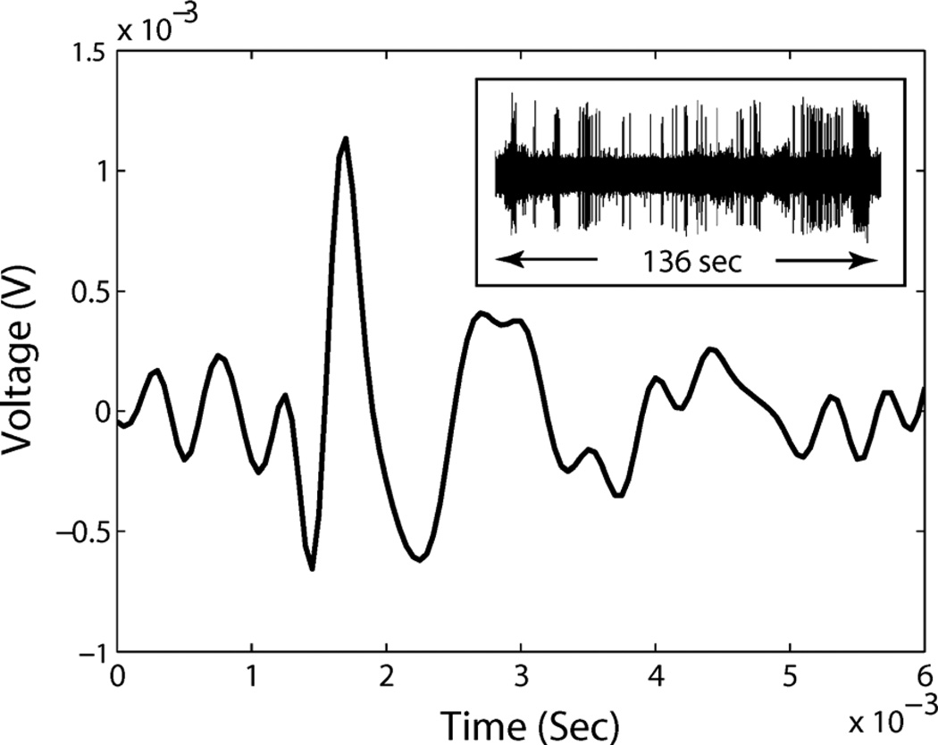
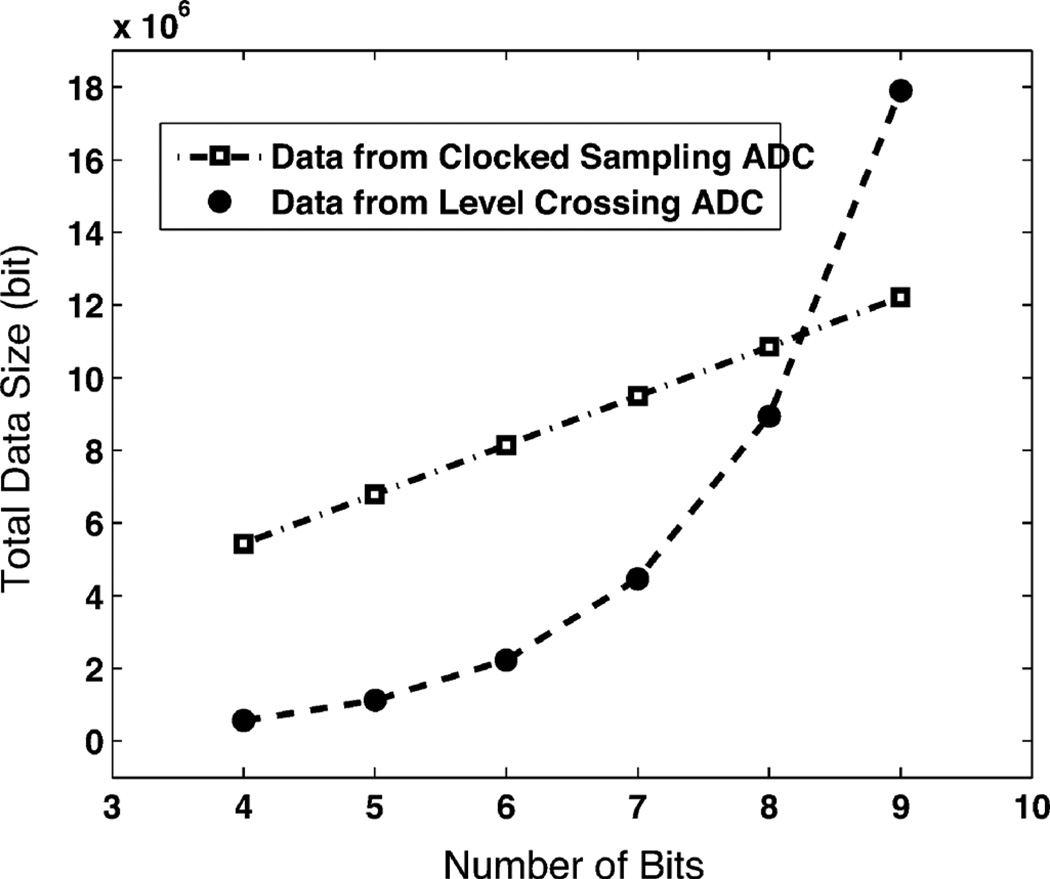
From the above discussion, we conclude that the level crossing sampling method will generate less data than the clocked sampling method, when the resolution requirement is low and the signal has a small activity ratio. This property fits the specified bio-potential recording applications very well. In Fig. 7, a rat cortex signal with a zoom-in spike is shown. The activity ratio of the signal is 0.12. When we apply this signal to both a level crossing ADC and a clocked sampling ADC with a standard 20 kS/s sampling rate, the total data size is related to the resolution, and is compared in Fig. 8. At 7-bits resolution, continuous time level crossing sampling can save 40%–60% of the data size over the clocked sampling method. In the current recording system, the input referred noise is at a 10 µV level without a probe, while the peak of a spike signal is at the mV level, so a 6–7 bit resolution is reasonable.
Fig. 7.
A recorded rat cortex signal spike and its long time behavior. The single spike duration is about 0.5 ms. The activity ratio of the signal is 0.12.
Fig. 8.
Data size comparison of a level crossing sampling ADC (this work) and a clocked sampling ADC (20 kS/s) when recording a 136 second rat cortex signal. From the level crossing sampling ADC, the number of events is exponentially proportional to the number of the resolution bits. Because bio-potential signals have a low activity ratio, the data size can be saved by 50% or more when the resolution is under 7 bit.
C. Level-Crossing vs. Integrated-and-Fire
Integrated-and-fire [12] is another method to convert an analog signal into asynchronous digital pulses. In [13]–[15], Harris et al. proposed the integrated-and-fire method for bio-potential recording. Similar with the fixed-window level crossing method, the integrated-and-fire method also provides a solution to avoid changing reference voltages in order to reduce circuit complexity and power consumption. In this method, the output pulse frequency is proportional to the absolute amplitude of the input signal, while in the level-crossing method, the output pulse frequency is proportional to the slope of the input signal. Therefore, the level crossing sampling method has advantages for saving power and resisting dc offset voltage, since the integrated-and-fire method will keep generating pulses if there is a background low frequency component in the input signal.
D. Asynchronous Transmitter vs. Synchronous Transmitter
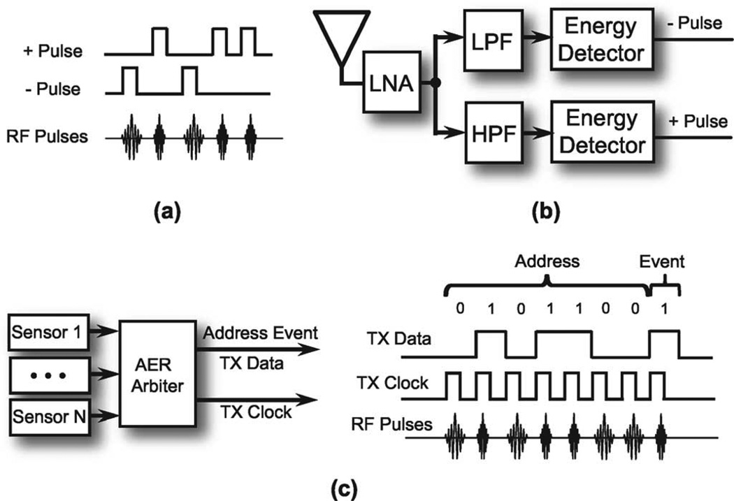
The level crossing sampling ADC outputs are two sequences of asynchronous digital pulse chains. Traditional synchronous transmission will compromise the advantage from the asynchronous sampling. In such a case, asynchronous wireless transmission should be implemented. A feasible solution could be an FSK-OOK UWB impulse radio [40]. As show in Fig. 9(a), the positive pulse and negative pulse are carried by different frequency carriers. The polarity of the received impulses will be distinguished by filters and demodulated by envelope detectors as shown in Fig. 9(b), and finally digitized by level-crossing quantizers. If a multi-channel sensor array is applied, the wireless address event representation [41] could be used, in which a local clock for coding will help to add address bits to the asynchronous data packet, as shown in Fig. 9(c). In order to save power, the local clock should be running only when there is a data packet to send. The clock and data recovery method for the asynchronous wireless solution is described in [40].
Fig. 9.
Asynchronous wireless transmission solution for level crossing sensors, (a) Asynchronous FSK-OOK impulse radio modulation, (b) FSK-OOK demodulation, (c) Wireless Address Event Representation for sensor array, Address Event Sensor Array Data Package and Modulation.
III. System and Circuit Design
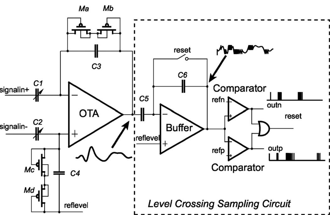
We proposed the new fixed window level-crossing ADC design by resetting the input signal, instead of changing the threshold voltages using DACs in each channel. Fig. 10 is the block diagram of the bio-potential recording circuit using the continuous time fixed window level crossing sampling method. The integrated circuit contains a low-power low-noise bio-potential amplifier (OTA) and a level crossing sampling analog to digital converter (Level Crossing Sampling Circuit). The OTA is used as the main amplifier. Capacitor feedback is designed to work with the OTA to reject the low frequency variation of the input neural signal. The bandwidth of the OTA with feedback is 200 Hz–20 kHz. Ma-Md are utilized as large pseudo-resistors to amplify low frequency signals while rejecting dc offsets. In the feedback, C1 and C2 are tunable capacitors in order to control the gain of the front end, which can be selected as 7 pF or 35 pF. Feedback capacitor C3 and C4 are 50 fF. Both C5 and C6 are 1 pF. The ratio between C1 and C3 should be made large enough to increase the gain, so input capacitor C1 and C2 occupies large silicon area on chip. This OTA is designed based on [42].
Fig. 10.
Schematic of the bio-potential recording chip with typical waveform at different nodes. The capacitor feedback of the amplifier is designed to filter out the dc component of the input signal while rejecting common-mode noise. C1 and C2 are tunable capacitors for changing the gain. The MOS-bipolar pseu-doresistor elements are working as large resistors to amplify low frequency signal and reject the dc offset. The amplified analog signal is compared with the threshold voltages. When the comparator triggers, a digital pulse is sent to the output and the level crossing sampling circuit is reset.
A. Level Crossing Sampling ADC
In Fig. 10, if the analog input signal is zero, the output of the Buffer will be set to reflevel. Two threshold voltages (refn and refp) are compared with the buffer output. The gap between the threshold voltages (refn or refp) and reference level (reflevel) is the positive or negative delta step. The amplified signal is sampled when its amplitude is higher than refn or lower than refp. When the amplitude of the input signal is crossing the window between refn and refp, one of the comparator outputs (outn or outp) as well as the reset signal will be set to VDD. The high reset output will reset the buffer output to reflevel. After reset, the outputs of the comparators will be logic low because reflevel is in the window between the two threshold voltages. So the reset signal is released to make the buffer return to the follower mode automatically. After reset, a voltage difference between the amplifier output and reflevel might exist, but this difference will be considered as a dc difference and hence can not pass the buffer with capacitor feedback. By doing so the amplitude is subtracted by a delta step. This process will generate a pulse from one of the comparator outputs (outn or outp). The comparator output pulses are the result of the level crossing sampling analog to digital conversion. The pulse rate is directly proportional to the rate of the signal change. The self-reset scheme makes the circuit a clock-less A/D converter.
B. Front-End Amplifier, Buffer and Comparators
The resolution of the level crossing sampling ADC is determined by the delta amplitude and timing preciseness of the resetting process. The system expects a shorter duration of the reset pulse for a higher resolution. The duration of the reset pulse is the sum of the responding time of the comparator and the resetting time of the Level Crossing Sampling Circuit. A high-speed unity gain Buffer is inserted between OTA and Level Crossing Sampling Circuit in order to perform fast resetting. The simulation result shows that the pulse width is 30 ns. The threshold level step can be reduced to 4 mV. The quantization circuit could reach 5 bits resolution.
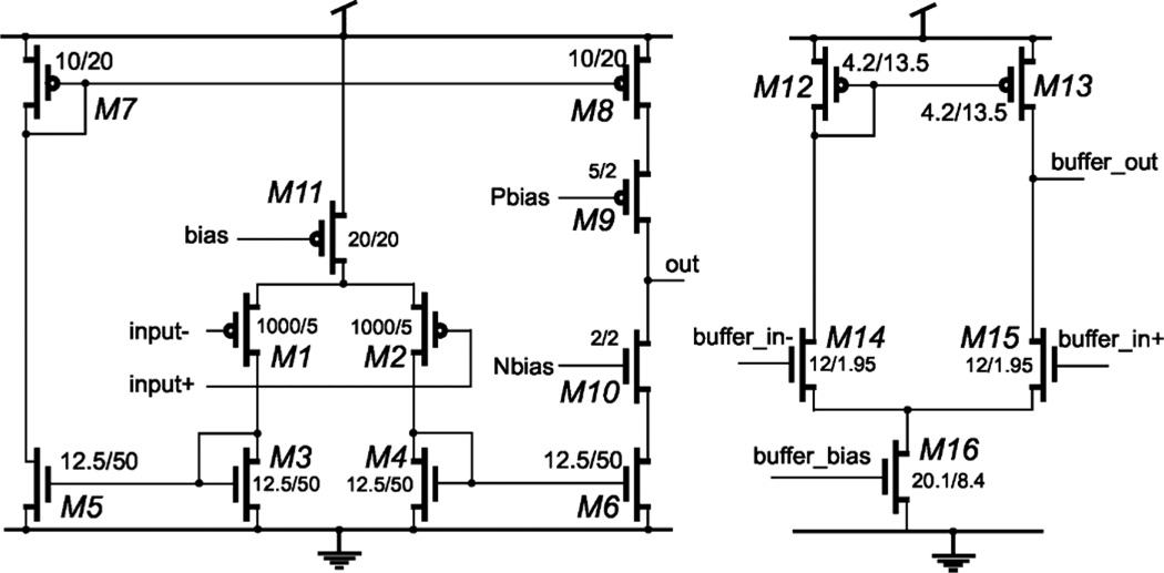
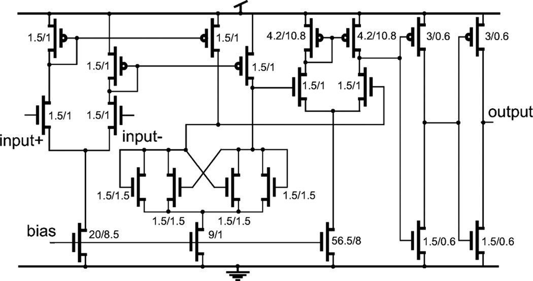
The schematics of the OTA and the Buffer are shown in Fig. 11. The bias current of Mll is set to 5 µA and current in M1-M10 is 2.5 µA. A cascade structure is used in the output stage to boost the gain. The circuit is designed to suppress noise while maintaining relevant speed for neural signal processing. The W/L ratio of the input differential PMOS transistor pair is large (1000 µm/5 µm) in order to reduce input referred noise. The open loop gain of the OTA is 94 dB from simulation. A high-performance comparator [43] including preamplifier, decision circuit and output buffer is implemented. The schematic of the comparator is shown in Fig. 12. According to the simulation results, the comparator consumes 23 µA. The rising time and falling time of the pulse is 2 ns and 3.5 ns, respectively. The rising time and falling time will increase to 7 ns and 8 ns if the output of the comparator drives output pads. The simulated propagation delay of the comparator is 7 ns, 10 ns, and 23 ns for input slopes of 2000 V/ms, 32 V/ms and 2 V/ms, respectively. The minimum and maximum pulse width from the comparator output is 27 ns and 31.5 ns, respectively. The pulse width represents the loop delay time Tloop of the delta modulator, which includes the resetting time of the buffer. As discussed in Section II, the decision time of the comparator will affect the system resolution. A fast comparator is expected when higher resolution is desired. The offset of the comparator will add to the offest-error to the system. However, if the offset is a fixed value, it will only cause a gain error at the reconstructed waveform, which can be removed by calibration.
Fig. 11.
Schematic of the low-power low-noise operational amplifier (OTA) and the Buffer with the sizes (W/L ratio) of the devices. The input stage of the OTA is a PMOS pair to reduce noise. The output stage of the OTA is a cascade amplifier to increase the gain.
Fig. 12.
Schematic of the comparator used in the design, including preampliffier decision circuit and output buffer. All ratios (W/L) are given in micrometers.
IV. Hardware Test-Bed
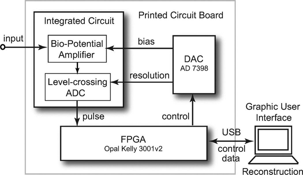
A diagram of the hardware test-bed is shown in Fig. 13. The entire system is powered at 3.3 V. The digital interface was provided by a field programmable gate array (FPGA) on an Opal Kelly 3001v2 board. The bias voltage was provided by an Analog Device AD7398 12 bit DAC. The FPGA samples the output pulses from the level crossing sampling ADC using a 50 MHz clock. A counter is used to measure the time stamp between two consecutive pulses. When a pulse is detected, its polarity and the time stamp between this pulse and the previous pulse will be recorded in the RAM of the FPGA. A double buffer is used in the RAM so the pulse recording and transmitting are able to work continuously without losing data. The data of the pulse polarity and time stamp is sent to the computer through a universal serial bus (USB) 2.0 cable. The entire system consists of two stacked printed circuit boards (PCB) packaged in a shielded box.
Fig. 13.
A block diagram of the hardware test board. The test board consists of a DAC and a Spartan-3 FPGA. The bio-potential recording chip is controlled using a GUI driven C++ program.
Reconstruction of the recorded signal from the pulse sequence is performed by the computer. According to the timing of the positive and negative pulses, the recorded waveform value is increased by a positive delta with each positive pulse, and decreased by a negative delta with each negative pulse. Plotting the recorded value with the time stamp reconstructs the original signal. Accumulation of the offsets will cause a dc shift in the reconstructed waveform. In this test-bed, the dc shift is removed by a high pass digital filtering with cutoff frequency at 2 Hz.
V. Experimental Results
The circuit was fabricated using the AMI 0.5 µm 3M2P process. The feedback capacitors are built of PIP (polysilicon-insultor-polysilicon) structure. The measured gain of the bio-potential amplifier with feedback is 53 dB between 200 Hz and 20 kHz. In this bandwidth, the input referred noise is 20 with rms of 2.8 µV. The input-referred noise is calculated from the measured output noise and amplifier gain. The experimental results show that the cross talking between channels can be ignored.
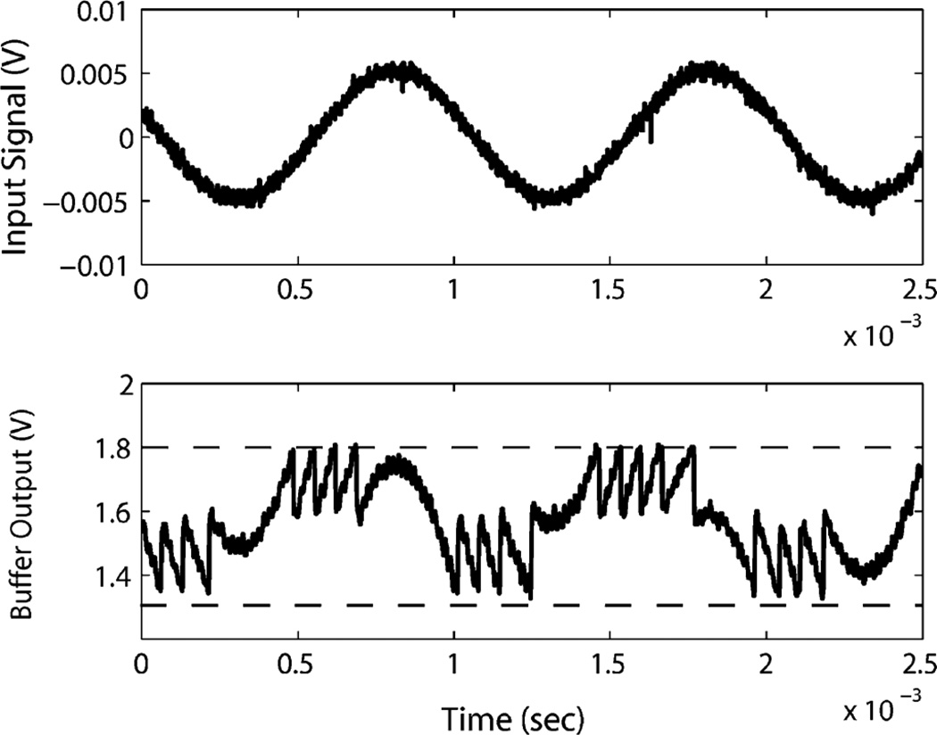
For a 3.3 V power supply, the reference level (reflevel) is set to 1.65 V. Fig. 14 shows the measured input and output waveform of the amplifier and analog buffer output. The input signal is a 1 kHz 10 mV peak-to-peak sine wave. Referring to Fig. 10, the buffer output signal is compared with the positive (1.8 V) and negative (1.35V) threshold voltages. Here the positive and negative delta step have different values. This will be considered during reconstruction in the digital domain. Ideally, different values of the delta step will not affect the recording and reconstruction. However, the individual pulse width varies with the delta step amplitude due to the common mode voltage of the comparator. Although this variation (less than 5 ns by simulation) is small compared to the pulse width (about 30 ns by simulation), it should be minimized in order to have a higher signal to noise ratio. Therefore, in the clinical recording the positive and negative delta step should be equal. It should be noted that, for a periodic signal, when the input signal amplitude is not integral times of the delta step, the number of the output pulses in one period will be different than in the other periods. Just as shown in Fig. 14, one period has four rising pulses while the other has five rising pulses. This will not affect the reconstruction of the waveform.
Fig. 14.
Measured chip input and output waveform with 3.3 V single power supply. Top: 1 kHz input signal with amplitude of 10 mV. Bottom: Analog output signal from the buffer, which is the input signal amplified then subtracted by a delta level step. The positive threshold is 1.8 V and negative threshold is 1.35 V. Reference level (reflevel) is 1.65 V.
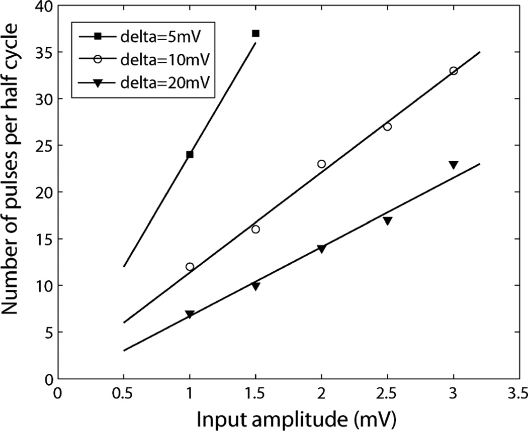
We measured the number of output pulses as illustrated in Fig. 15. We used a 1 kHz sine signal as the input signal and set the delta step to 5 mV, 10 mV and 20 mV, and counted the number of output pulses at reset when the input changes from peak to peak (half cycle of the sine wave). When the delta level step is fixed, the number of the pulses is linearly proportional with the input signal amplitude, and is reversely proportional to the delta step when the signal amplitude is fixed.
Fig. 15.
Measured linearity of level crossing sampling ADC. The input signal is a 1 kHz sine wave. The total number of the pulses is proportional to the input signal amplitude. When the signal amplitude is fixed, the total number of the output pulses is reversely proportional to the delta level step.
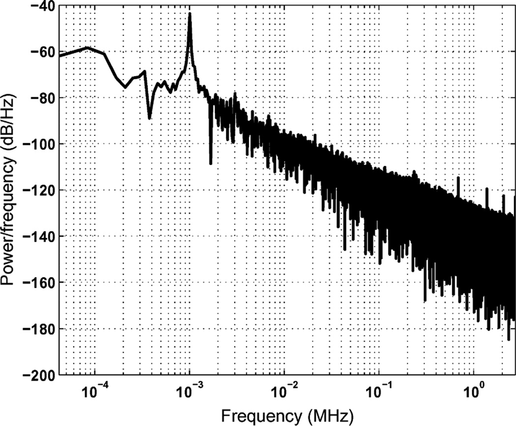
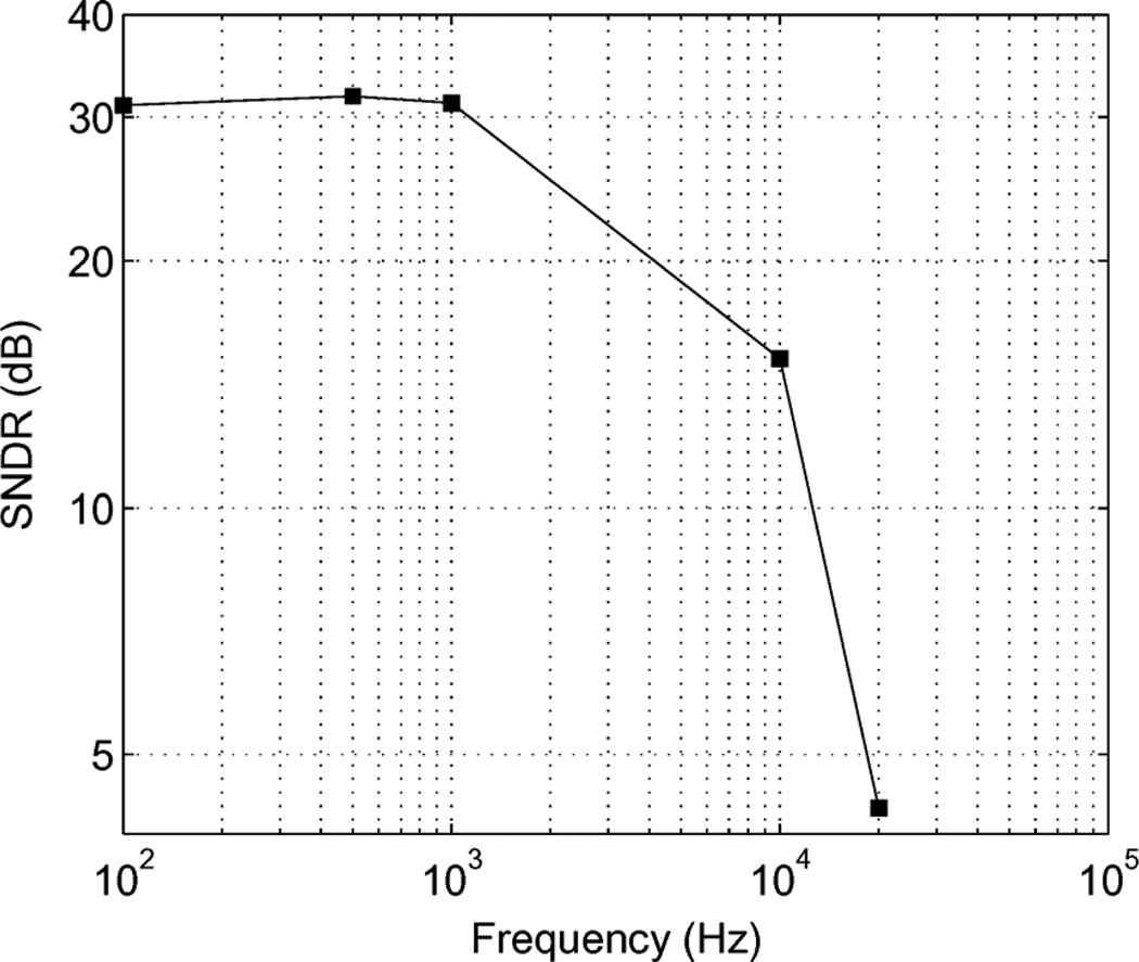
The power spectral density of the reconstructed sine waveform is plotted in Fig. 16. The measured signal to noise ratio is 31 dB for a 1 kHz input signal. The input signal range of the ADC is up to 5 kHz, as shown in Fig. 17.
Fig. 16.
Power spectrum density of the reconstructed waveform. The input signal is a 1 kHz sine wave with 6 mV peak to peak amplitude.
Fig. 17.
Compared signal to noise ratio versus frequency tested using a 7 mV sine waveform input.
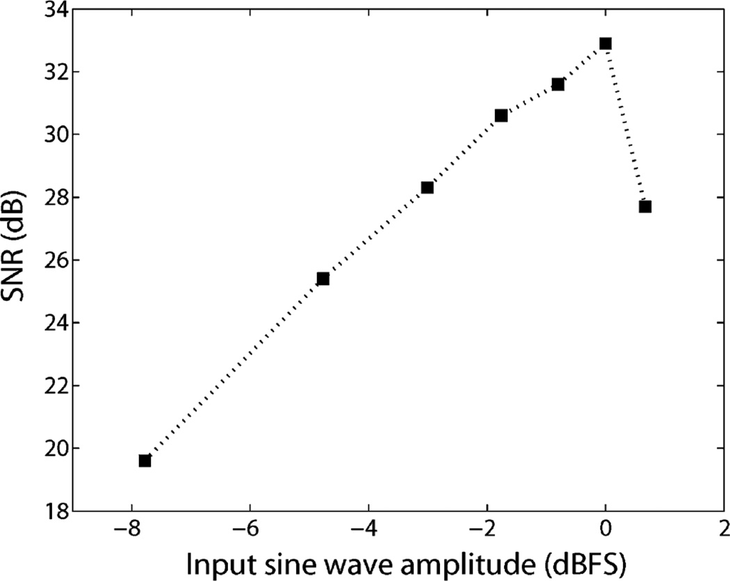
The signal to noise ratio of the reconstructed waveform as a function of the input signal amplitude is shown in Fig. 18. The 0 dBFS is 6 mV full scale amplitude. The measured SNR is smaller than the ideal case because of the finite loop delay time of the level crossing sampling circuit.
Fig. 18.
Measured signal to noise ratio of the reconstructed sine wave from the level crossing ADC as a function of input signal amplitude. The amplifier is saturated if the input signal is more than 7 mV. The 0 dBFS refers to 6 mV full-scale input amplitude.
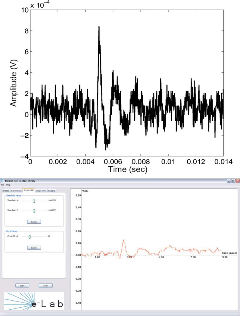
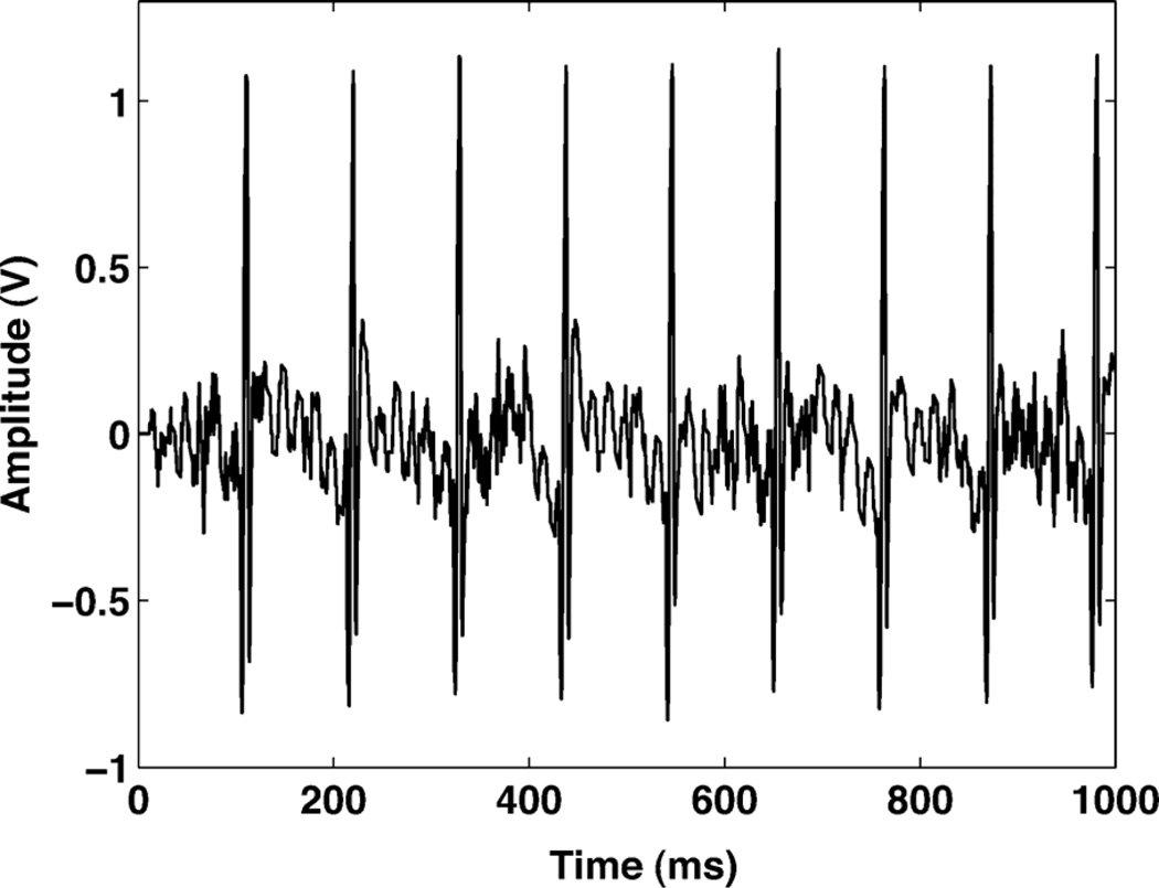
A demonstration system is developed with the hardware testbed. A graphical user interface (GUI) reconstructs the pulse sequence back to an analog waveform using zero order hold recovery. The GUI programmed using C++ is also controlling the bias of the amplifier and the delta amplitude of the level crossing ADC. The system is running in real-time monitoring the activities of the input signal. In the demo system, the positive and negative delta steps are not necessarily identical. The differences of positive and negative delta step can be controlled in software, and compensated when the reconstructed signal is displayed. Fig. 19 shows a reconstructed rat barrel cortex signal, which is generated from an Agilent 33250 arbitrary signal generator. The peak spike is 1 mV amplitude with 0.6 ms duration. We also used the testing system to record a mouse electrocardiograph (ECG) activity. The recorded waveform is shown in Fig. 20. Table I summarizes the main properties of the chip. The power consumption is measured with a 1 kHz 5 mV input sine wave.
Fig. 19.
Reconstructed waveform in GUI, running in real time. Top: neural signal of a rat barrel cortex from signal generator. Bottom: reconstructed waveform in GUI.
Fig. 20.
An ECG signal recorded from an in vivo experiment on a mouse.
TABLE I.
Measured Performance Summary
| Process technology | AMI 0.5µm CMOS |
| Chip size | 1.5mm by 1.5mm |
| Supply voltage | 3.3V |
| Amplifier Bandwidth | 200Hz-20kHz |
| Amplifier Gain | 53dB |
| Amplifier Output swing | 2.2V |
| Input-referred rms noise | 2.8µV |
| Amplifier power (4-channel) | 75.9µW |
| Sampling Method | Level-crossing sampling |
| Resolution | 5 bit |
| Reconstruction Method | Software |
| Chip power* (4-channel static) | 118.8µW |
| Chip power* (4-channel pulse rate 240k/sec total) | 501.6µW |
| Conversion Efficiency | 1.6nJ/conversion |
including ADC, front-end amplifier and buffer
A general comparison is made with recently reported asynchronous ADCs and biomedical recording ADCs, as shown in Table II. As we discussed in Section I, the most important parameters in a bio-potential sensor front end circuit are the power consumption, data compression rate and silicon area. We define a figure of merit (FOM) as
| (9) |
Where D is the data compression rate and A is the silicon area of the ADC. The signal to noise and distortion ratio SNDR is in the ratio form not dB. In this FOM calculation, the level crossing sampling ADC has a data compression rate D of 50% while the data compression rate of clocked ADC is set at 1. The FOM is listed in Table II. It should be noticed that due to the process limitation, the FOM of our fixed window level crossing ADC is not the best in Table II. However, its low complexity, low power and data compression advantages are very helpful if large scale sensors are integrated with wireless capability, especially when advanced processing technology is applied. In the large scale sensor array, each sensor will be tracking signals with a small activity ratio. A fixed window level crossing ADC is a competitive candidate in this situation, since no local DAC or clock is necessary in the individual sensor.
TABLE II.
Performance Comparison of ADCs Recently Reported for Sensory Applications
| Year | 2012 | 2008 | 2011 | 2006 | 2010 |
|---|---|---|---|---|---|
| Integrated Circuit Technology | 0.5µm CMOS | 90nm CMOS | 0.18µm CMOS not fully integrated | 0.6µm CMOS simulation | 0.13µm CMOS |
| Power Supply | 3.3V | IV | 0.7V | 5V | 1.2V |
| ADC Area | 0.06mm2 | 0.06mm2 | 0.96mm2 | N/A | 0.17mm2 |
| ADC Method | Fixed Window Asynchronous | Floating Window Asynchronous | Floating Window Asynchronous | Integration Asynchronous | SAR ADC Clocked |
| Input Signal Bandwidth | 0.2–5kHz | 0.2–3.4kHz (Audio) | 1kHz (full scale) | 5.4kHz | N/A |
| Measured SNDR | 31dB | 50 dB | 43.2 dB | N/A | 39.32dB |
| Power Consumption | 8.25µW (Static) 106µW (1kHz Input) |
45µW (ADC only) |
25µW w/o off chip logic |
100 µW simulation | 1µW |
| Conversion Rate (per second) | 60k | 512ka | 50k | 10k | |
| Figure of Merit (l/nj · mm2) | 662bc | 1,048,646c | 601bcd | N/A | 5379e |
| Reference | This Work | [39] | [23] | [15] | [9] |
Level crossing sampling with 8bit resolution for 1kHz input signal
Using off-line reconstruction
SNDR is set to 1kHz input signal
Digital logic feedback not integrated on chip
Using clocked ADC, no data compression
VI. Conclusion
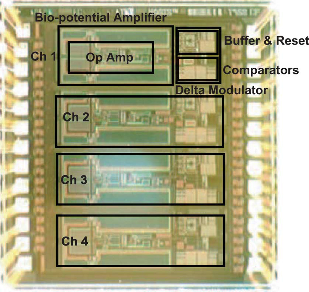
We investigated the level crossing sampling ADC and compared its performance with traditional clocked sampling ADCs. In the application of bio-potential recording systems, level crossing ADCs generate less data than clocked sampling ADCs while keeping the same resolution. This happens when the signal has a small activity ratio and the quantization of the system has a low resolution. We designed and tested the fabricated 4-channel low-power low-noise bio-potential recording system. Our fixed window level crossing ADC doesn’t need local DACs to track the input signal, which saves power and silicon area. The chip micrograph is illustrated in Fig. 21. The chip area is 1.5 mm by 1.5 mm. The test result shows that our circuit with all four channels consumes 118.8 µW in static mode and 501.6 µW when the pulse rate is at 60 kS/sec in each channel (total 240 kS/sec), while the input signal is a 1 kHz sine wave with 5 mV Vpp. The equivalent conversion efficiency is 1.6 nJ/conversion. The ADC resolution is 5–6 bit. The resolution can be improved by using better process technology. When the signal activity ratio is 0.12, the level crossing sampling ADC can reduce 60% data size than clocked sampling ADC while keeping the same resolution. We demonstrated the system performance in a real mouse ECG recording experiment. The system provides remarkable data compression, clock-less A/D conversion and low power consumption. This design is a competitive solution in large scale wireless bio-potential recording systems.
Fig. 21.
Chip micrograph with main building blocks highlighted.
Acknowledgment
The support of MOSIS in chip fabrication is gratefully acknowledged. The authors also thank Prof. Fred Sigworth, Prof. Peter Kindlmann, and Dr. Selcuk Talay for their discussion and help with the chip measurement.
This work was supported by ONR under Grants 439471 and 396490, and NSF Award 0649349. This paper was recommended by Associate Editor S. R. Sonkusale.
Biographies

Wei Tang (S’06) received the B.S. degree in electronics engineering from Department of Microelectronics in Peking University, China, in 2006 and the M.S. and Ph.D. degrees in electrical engineering from Yale University, New Haven, CT, in 2009 and 2012, respectively.
He joined Klipsh School of Electrical and Computer Engineering at New Mexico State University, Las Cruces, in 2012 as an Assistant Professor. His research interests are analog/mixed-signal and low-power circuit design, wireless communication circuit design, and testing for biomedical applications.

Ahmad Osman received a B.S. degree in 2009 in biomedical engineering from the University of Hartford, CT. He will receive a M.S. degree in biomedical engineering with a concentration in bioinstrumentation and bioimaging in 2012 from the University of Connecticut, Storrs.
He was a chemistry and biology Teacher Assistant at the University of Hartford, 2008–2011. Currently he is a Research Assistant at the Yale University/John B. Pierce Laboratory, working with Dr. Vincent Pieribone. His laboratory studies the electrical activity of the brain by developing instruments to make optical recordings of neuronal membrane potential possible in freely awake moving animals.

Dongsoo Kim (M’02) received the M.S. and Ph.D. degrees in electrical and electronics engineering from Yonsei University, Seoul, Korea, in 2004 and 2008, respectively.
Currently, he works as a Staff Analog Design Engineer at Aptina Imaging, San Jose, CA. From 2008 to 2010, he was a Postdoctoral Associate in the Department of Electrical Engineering, Yale University, New Haven, CT. His research interests include CMOS image sensors, smart sensors, low-noise circuit design, and biomedical instrumentation.

Brian Goldstein (GS’08) received the B. S. degree in computer and systems engineering and computer science in 2006 from Rensselaer Polytechnic Institute, Troy, NY. He received the M.S. and M.Phil. degree in electrical engineering from Yale University, New Haven, CT in 2010 and 2011, respectively, and is currently a graduate student working toward the Ph.D. degree.
From 2006 to 2008 he worked on embedded systems at Goodrich Pump & Engine Control Systems, N.A. in West Hartford, CT. His research interests include analog and mixed-signal integrated circuits, low-noise circuit design, and systems engineering for biomedical applications.

Chenxi Huang received the B.S. degree in electrical engineering from Shanghai Jiaotong University, China, in 2008 and the M.S. degree in electrical engineering from Yale University, New Haven, CT, in 2009. She is currently working toward the Ph.D. degree in biomedical engineering from Yale University.
From 2008 to 2009, she was with the eLab at Yale, working on small signal amplification systems. Her current research interests are image processing, optimization, estimation theory, and hypothesis testing on single particle reconstruction.

Berin Martini received the B.Sc. degree with Honours in physics from University of Melbourne, Australia, in 2001.
He worked for the Defence Science and Technology Organisation (DSTO) for a number of year until 2007, when he started working at eLab at Yale University, New Haven, CT, and then Purdue University, West Lafayette, IN, as a Research Associate.

Vincent A. Pieribone attended New York University College of Arts and Sciences where he received a baccalaureate degree in biology and chemistry in 1986. He then attend New York University’s Graduate School of Arts and Sciences and received his doctorate in Philosophy in 1992 in neuroanatomy and neurophysiology.
From 1990 to 1992 he was a National Science Foundation and Fogarty International Fellow at the Nobel Institute of Neurophysiology at the Karolinska Institute in Stockholm Sweden. From Sweden he did postdoctoral work at Rockefeller University in New York from 1992 to 1995 and became an Assistant Professor there in 1995. He joined the Pierce laboratory in December 1997.

Eugenio Culurciello (S’97–M’99) received the Ph.D. degree in electrical and computer engineering in 2004 from the Johns Hopkins University, Baltimore, MD.
He is an Associate Professor of the Weldon School of Biomedical Engineering and an Associate Professor of Psychological Sciences in the College of Health & Human Sciences at Purdue University, West Lafayette, IN, where he directs the e-Lab laboratory. He is the author of Silicon-on-Sapphire Circuits and Systems, Sensor and Biosensor Interfaces (McGraw-Hill, 2009). His research interest is in analog and mixed-mode integrated circuits for biomedical instrumentation, synthetic vision, bio-inspired sensory systems and networks, biological sensors, silicon-on-insulator design.
Dr. Culurciello is the recipient of The Presidential Early Career Award for Scientists and Engineers (PECASE) and Young Investigator Program from ONR, the Distinguished Lecturer of the IEEE (CASS),
Footnotes
Color versions of one or more of the figures in this paper are available online at http://ieeexplore.ieee.org.
Contributor Information
Wei Tang, Klipsch School of Electrical and Computer Engineering, New Mexico State University, Las Cruces NM 88011 USA.
Ahmad Osman, John B. Pierce Laboratory, Yale University, New Haven CT 06511 USA.
Dongsoo Kim, School of Engineering and Applied Science, Yale University, New Haven CT 06511 USA.
Brian Goldstein, School of Engineering and Applied Science, Yale University, New Haven CT 06511 USA.
Chenxi Huang, School of Engineering and Applied Science, Yale University, New Haven CT 06511 USA.
Berin Martini, Weldon School of Biomedical Engineering, Purdue University, West Lafayette, IN 47907 USA.
Vincent A. Pieribone, John B. Pierce Laboratory, Yale University, New Haven CT 06511 USA
Eugenio Culurciello, Email: euge@purdue.edu, Weldon School of Biomedical Engineering, Purdue University, West Lafayette, IN 47907 USA.
References
- 1.Wise K, Anderson D, Hetke J, Kipke D, Najafi K. Wireless implantable microsystems: High-density electronic interfaces to the nervous system. Proc. IEEE. 2004 Jan;vol. 92(no. 1.):76–97. [Google Scholar]
- 2.Harrison RR, Watkins PT, Kier RJ, Lovejoy RO, Black DJ, Greger B, Solzbacher F. A low-power integrated circuit for a wireless 100-electrode neural recording system. IEEE J. Solid-State Circuits. 2007 Jan:123–133. [Google Scholar]
- 3.Greenwald E, Mollazadeh M, Thakor N, Tang W, Culurciello E. A vlsi neural monitoring system with ultra-wideband telemetry for awake behaving subjects; Proc. 2010 IEEE Int. Symp. Circuits Syst. (ISCAS); 2010. Jun 2, pp. 1193–1196. [DOI] [PubMed] [Google Scholar]
- 4.Nurmikko A, Donoghue J, Hochberg L, Patterson W, Song Y-K, Bull C, Borton D, Laiwalla F, Park S, Ming Y, Aceros J. Listening to brain microcircuits for interfacing with external world: Progress in wireless implantable microelectronic neuroengineering devices. Proc. IEEE. 2010 Mar;vol. 98(no. 3):375–388. doi: 10.1109/JPROC.2009.2038949. [DOI] [PMC free article] [PubMed] [Google Scholar]
- 5.Guan K, Singer A. A level-crossing sampling scheme for non-bandlimited signals. Proc. 2006 IEEE Int. Conf. Acoust., Speech, Signal Process. (ICASSP 2006) 2006 May;vol. 3:III 381–III 383. [Google Scholar]
- 6.Chae M, Liu W, Yang Z, Chen T, Kim J, Sivaprakasam M, Yuce M. A 128-channel 6 mw wireless neural recording ic with on-thefly spike sorting and uwb tansmitter; IEEE Int. Solid-State Circuits Conf. Dig. Tech. Papers (ISSCC); 2008. Feb, pp. 146–603. [Google Scholar]
- 7.Chestek C, Gilja V, Nuyujukian P, Kier R, Solzbacher F, Ryu S, Harrison R, Shenoy K. Hermesc: Low-power wireless neural recording system for freely moving primates. IEEE Trans. Neural Syst. Rehab. Eng. 2009 Aug;vol. 17(no. 4):330–338. doi: 10.1109/TNSRE.2009.2023293. [DOI] [PubMed] [Google Scholar]
- 8.O’Driscoll S, Meng T. Adaptive resolution ADC array for neural implant; Proc. Annu. Int. Conf. IEEE Eng. Med. Biol. Soc. (EMBC); 2009. Sep, pp. 1053–1056. [DOI] [PubMed] [Google Scholar]
- 9.Yeager D, Zhang F, Zarrasvand A, George N, Daniel T, Otis B. A 9 a, addressable gen2 sensor tag for biosignal acquisition. IEEE Solid- State J Circuits. 2010 Oct;vol. 45(no. 10):2198–2209. [Google Scholar]
- 10.Walker R, Gao H, Nuyujukian P, Makinwa K, Shenoy K, Meng T, Murmann B. A 96-channel full data rate direct neural interface in 0.13 um cmos; Proc. Symp. VLSI Circuits (VLSIC); 2011. Jun, pp. 144–145. [Google Scholar]
- 11.Chen S, Tang W, Culurciello E. A 64 × 64 pixels uwb wireless temporal-difference digital image sensor; Proc. 2010 IEEE Int. Symp. Circuits Syst. (ISCAS); 2010. Jun 2, pp. 1404–1407. [Google Scholar]
- 12.Vandeursen JM, Peperstraete JA. Analog-to-digital conversion based on a voltage-to-frequency converter. IEEE Trans. Ind. Electron. Control Instrum. 1979 Augvol. IECI-26(no. 3):161–166. [Google Scholar]
- 13.Harris J, Principe J, Sanchez J, Chen D, She C. Pulse-based signal compression for implanted neural recording systems; Proc. IEEE Int. Symp. Circuits Syst. (ISCAS); 2008. May, pp. 344–347. [Google Scholar]
- 14.Chen D, Harris J, Principe J. A bio-amplifier with pulse output. Proc. 26th Annu. Int. Conf. IEEE Eng. Med. Biol. Soc. (IEMBS) 2004 Sep;vol. 2:4071–1074. doi: 10.1109/IEMBS.2004.1404136. [DOI] [PubMed] [Google Scholar]
- 15.Chen D, Li Y, Xu D, Harris J, Principe J. Asynchronous biphasic pulse signal coding and its CMOS realization; Proc. IEEE Int. Symp. Circuits Syst. (ISCAS); 2006. May, pp. 2293–2296. [Google Scholar]
- 16.Trakimas M, Sonkusale S. A 0.8 v asynchronous ADC for energy constrained sensing applications; Proc. IEEE Custom Integr. Circuits Conf. (CICC); 2008. Sep, pp. 173–176. [Google Scholar]
- 17.Tang W, Culurciello E. A pulse-based amplifier and data converter for bio-potentials; Proc. IEEE Int. Symp. Circuits Syst. (ISCAS); 2009. May, pp. 337–340. [Google Scholar]
- 18.Tang W, Huang C, Kim D, Martini B, Culurciello E. 4-channel asynchronous bio-potential recording system; Proc. 2010 IEEE Int. Symp. Circuits Syst. (ISCAS); 2010. Jun 2, pp. 953–956. [Google Scholar]
- 19.Trakimas M, Sonkusale S. A 0.5 v bulk-input operational transconductance amplifier with improved common-mode feedback; Proc. IEEE Int. Symp. Circuits Syst. (ISCAS); 2007. May, pp. 2224–2227. [Google Scholar]
- 20.Agarwal R, Trakimas M, Sonkusale S. Adaptive asynchronous analog to digital conversion for compressed biomedical sensing; Proc. IEEE Biomed. Circuits Syst. Conf. (BioCAS); 2009. Nov, pp. 69–72. [Google Scholar]
- 21.Kurchuk M, Tsividis Y. Signal-dependent variable-resolution clockless a/d conversion with application to continuous-time digital signal processing. IEEE Trans. Circuits Syst. I Reg. Papers. 2010 May;vol. 57(no. 5):982–991. [Google Scholar]
- 22.Hwang S, Trakimas M, Sonkusale S. A low-power asynchronousecg acquisition system in cmos technology; Proc. Annu. Int. Conf. IEEE Eng. Med. Biol. Soc. (EMBC); 2010. Sep 4, pp. 5262–5265. [DOI] [PubMed] [Google Scholar]
- 23.Trakimas M, Sonkusale S. An adaptive resolution asynchronous ADC architecture for data compression in energy constrained sensing applications. IEEE Trans. Circuits Syst. I, Reg. Papers. 2011 May;vol. 58(no. 5):921–934. [Google Scholar]
- 24.Trakimas M, Hwang S, Sonkusale S. Low power asynchronous data acquisition front end for wireless body sensor area network; Proc. 24th Int. Conf. VLSI Design (VLSI Design); 2011. Jan, pp. 244–249. [Google Scholar]
- 25.Inose H, Aoki T, Watanabe K. Asynchronous delta-modulation system. Electron. Lett. 1966 Mar;vol. 2(no. 3):95–96. [Google Scholar]
- 26.Sayiner N, Sorensen H, Viswanathan T. A level-crossing sampling scheme for a/d conversion. IEEE Trans. Circuits Syst. II, Analog Digit. Signal Process. 1996 Apr;vol. 43(no. 4):335–339. [Google Scholar]
- 27.Allier E, Sicard G, Fesquet L, Renaudin M. A new class of asynchronous a/d converters based on time quantization; Proc. 9th Int. Symp. Asynchronous Circuits Syst; 2003. May, pp. 196–205. [Google Scholar]
- 28.Jungwirth P, Poularikas A. Improved sayiner level crossing ADC; Proc. 36th Southeastern Symp. Syst. Theory; 2004. pp. 379–383. [Google Scholar]
- 29.Schell B, Tsividis Y. Analysis of continuous-time digital signal processors; Proc. IEEE Int. Symp. Circuits Syst. (ISCAS); 2007. May, pp. 2232–2235. [Google Scholar]
- 30.Guan K, Singer A. Opportunistic sampling of bursty signals by level-crossing—An information theoretical approach; Proc. 41st Annu. Conf. Inf. Sci. Syst. (CISS); 2007. Mar, pp. 701–707. [Google Scholar]
- 31.Akopyan F, Manohar R, Apsel A. A level-crossing flash asynchronous analog-to-digital converter; Proc. 12th IEEE Int. Symp. Asynchronous Circuits Syst; 2006. Mar, pp. 11–22. [Google Scholar]
- 32.Guan K, Singer A. Sequential placement of reference levels in a level-crossing analog-to-digital converter; Proc. 42ndAnnu. Conf. Inf. Sci. Syst. (CISS); 2008. Mar, pp. 464–469. [Google Scholar]
- 33.Fesquet L, Sicard G, Bidandgaray-Fesquet B. Targeting ul-tralow power consumption with non-uniform sampling and filtering; Proc 2010 IEEE Int. Symp. Circuits Syst. (ISCAS); 2010. Jun 2, pp. 3585–3588. [Google Scholar]
- 34.Foster J, Wang T-K. Speech coding using time code modulation. IEEE Proc. Southeastcon 91. 1991 Apr;vol. 2:861–863. [Google Scholar]
- 35.Kozmin K, Johansson J, Delsing J. Level-crossing ADCperformance evaluation toward ultrasound application. IEEE Trans. Circuits Syst. I, Reg. Papers. 2009 Aug;vol. 56(no. 8):1708–1719. [Google Scholar]
- 36.Wang T, Wang D, Hurst P, Levy B, Lewis S. A level-crossing analog-to-digital converter with triangular dither. IEEE Trans. Circuits Syst. I, Reg. Papers. 2009 Sep;vol. 56(no. 9):2089–2099. [Google Scholar]
- 37.Kurchuk M, Tsividis Y. Signal-dependent variable-resolution clockless a/d conversion with application to continuous-time digital signal processing. IEEE Trans. Circuits Syst. I, Reg. Papers. 2010 May;vol. 57(no. 5):982–991. [Google Scholar]
- 38.Agarwal G, Servi A, Eid F, Livermore C. Selective self-assembly of polymer structures using templated assembly by selective removal. IEEE Trans. Nanotechno.l. 2011 May;vol. 10(no. 3):617–625. [Google Scholar]
- 39.Schell B, Tsividis Y. A continuous-time ADC/DSP/ DAC system with no clock with activity-dependent power dissipation. IEEE J. Solid-State Circuits. 2008 Nov;vol. 43(no. 11):2472–2481. [Google Scholar]
- 40.Tang W, Culurciello E. A non-coherent fsk-ook uwb impulse radio transmitter for clock-less synchronization; Proc. IEEE Int. Symp. Circuits Syst. (ISCAS); 2011. May, pp. 1295–1298. [Google Scholar]
- 41.Folowosele MVF, Tapson J, Etienne-Cummings R. Wireless systems could improve neural prostheses. SPIE Newsroom. 2007 [Online]. Available: http://spie.org/xl6298.xml?highlight=x2416&articleid=xl6298.
- 42.Harrison RR, Charles C. A low-power low-noise cmos amplifier for neural recording applications. IEEE J. Solid-State Circuits. 2003;vol. 3 8:958–965. [Google Scholar]
- 43.Baker R. In: CMOS Circuit Design, Layout and Simulation. 2nd ed. Tewksbury SK, Brewer JE, editors. New York: Wiley-Interscience; 2007. ser. IEEE Press Series on Microelectronic Systems. [Google Scholar]


