

Abstract
The development of lensfree on-chip microscopy in the past decade has opened up various new possibilities for biomedical imaging across ultra-large fields of view using compact, portable, and cost-effective devices. However, until recently, its ability to resolve fine features and detect ultra-small particles has not rivalled the capabilities of the more expensive and bulky laboratory-grade optical microscopes. In this Frontier Review, we highlight the developments over the last two years that have enabled computational lensfree holographic on-chip microscopy to compete with and, in some cases, surpass conventional bright-field microscopy in its ability to image nano-scale objects across large fields of view, yielding giga-pixel phase and amplitude images. Lensfree microscopy has now achieved a numerical aperture as high as 0.92, with a spatial resolution as small as 225 nm across a large field of view e.g., >20 mm2. Furthermore, the combination of lensfree microscopy with self-assembled nanolenses, forming nano-catenoid minimal surfaces around individual nanoparticles has boosted the image contrast to levels high enough to permit bright-field imaging of individual particles smaller than 100 nm. These capabilities support a number of new applications, including, for example, the detection and sizing of individual virus particles using field-portable computational on-chip microscopes.
Introduction
The ability to image nano-scale structures is of critical importance in many fields, including biology, engineering, and materials science.1–5 However, the most ubiquitous mode of microscopy, bright-field optical microscopy, has limited resolution and contrast due to diffraction and possible aberrations.6 Hence the current gold standard for nano-imaging remains electron microscopy in both transmission (TEM) and scanning (SEM) modes, despite the required large capital investment, extensive sample preparation, and incompatibility with live-cell imaging. Scanning probe microscopy techniques7–12 may also be used, although they still require a large capital investment, involve long acquisition times, and are in general incompatible with live-cell imaging. To provide new solutions for high-resolution imaging needs, the last decade has seen the invention of several super-resolution optical techniques, including structured illumination micro-scopy,13–15 photoactivated localization microscopy (PALM),16 stochastic optical reconstruction microscopy (STORM),17 and stimulated emission depletion microscopy (STED).18,19 These techniques and others have uncovered various new phenomena in nano-biology, such as the nano-scale dynamics of cell adhesion and co-transcriptional folding of ribonucleic acids.20–22 Nonetheless, all of these imaging modalities suffer from complexity and relatively high cost, and more importantly, a small field of view (FOV) and depth of field that limit the throughput of these systems. Throughput and the ability to detect rare objects scattered over a large area are rather important in biomedical applications, such as the detection of viruses or parasites toward early disease diagnosis,23–25 as well as in various engineering applications, such as the characterization of nanowires or screening for structural defects during photomask fabrication.2 Furthermore, it is especially desirable to develop nano-imaging solutions that are compact, on-chip approaches, which are compatible with emerging optofluidic biosensors.25–29
In the past couple years, a new wide-field transmission imaging technique has emerged that can satisfy some of these requirements: lensfree computational on-chip microscopy. In lensfree on-chip microscopy,30–45 no lens is used between the sample and the detector (Fig. 1). Instead, the sample is placed in close proximity to the sensor-array, i.e., a CMOS (Complementary Metal-Oxide-Semiconductor) or a CCD (Charge-Coupled-Device) imager chip, and the sample’s shadow or in-line hologram is recorded/sampled. This on-chip imaging approach increases the FOV by orders of magnitude (especially when large format CCDs are used), and significantly reduces equipment complexity to the level of pocket-size field-portable devices.31–36 Recently, two main routes of lensfree transmission imaging have been undertaken: minimizing the sample-sensor distance to mitigate diffraction effects,39–42 and allowing moderate sample-sensor distances (e.g., <1–2 mm), while relying on computational holographic processing to digitally compensate for diffraction. The second approach, in particular, provides flexibility in experimental setup, and allows for example high-resolution 3D imaging and tracking of samples across large volumes.43–46 Through these two approaches, lensfree on-chip microscopy has already been applied to various biosensing applications, including, e.g., the design of a fluorometer,47 a study on the effect of drug treatments on cardiomyocytes,48 interferon-γ analysis for tuberculosis diagnosis,49 malaria diagnosis,35 and analysis of Papanicolaou tests.36
Fig. 1.
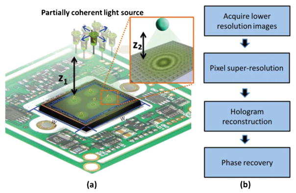
Lensfree on-chip microscopy. (a) A schematic diagram of the experimental setup. A partially coherent light source (e.g., a light-emitting-diode) positioned at distance z1 above the sample plane allows for holographic imaging, while lateral shifts of the source enable pixel-super-resolution. The small sample-to-sensor distance (z2) provides unit magnification and an ultra-large FOV, WX × WY that is equal to the active area of the opto-electronic sensor-chip. (b) Computational procedures for obtaining high-resolution on-chip images. Figure adapted from ref. 43.
In this Frontier Review, we discuss the recent achievements of lensfree holographic on-chip imaging in the observation of nano-scale objects. Recent bright-field transmission imaging experiments have demonstrated a compact and cost-effective platform that is insensitive to misalignments, and provides a wide FOV e.g., 20.5 mm2, a spatial resolution of 225 nm, and a detection sensitivity that is capable of imaging individual sub-100 nm particles when combined with a novel procedure involving the self-assembly of nanolenses forming nano-catenoid minimal surfaces around each nanoparticle. With these capabilities, lensfree computational on-chip microscopy can image various nano-scale objects, including, for example, individual viral particles or helical multi-walled carbon nanotubes. Below, we summarize the basic elements of lensfree computational on-chip microscopy, along with a summary of the recent experimental results demonstrating giga-pixel transmission imaging at the nano-scale.
Finally, we should note that we restrict this Frontier Review to bright-field on-chip nanoscopy only, and do not discuss fluorescent on-chip microscopy techniques since their state-of-the-art capabilities are currently unable to achieve deep sub-micron resolution or 3D imaging, unlike their lens-based or bright-field lensfree counterparts.43,50–52 Toward achieving a sub-micron resolution in 3D lensfree computational fluorescent imaging, we believe compressive sampling/sensing-based decoding approaches could be rather valuable.50,53,54 Unlike some misconceptions in the literature, these compressive sampling/sensing-based reconstruction approaches are not limited to only physically sparse objects. On the contrary, almost any object (or image), even though physically (or spatially) not sparse, can be represented in a sparse domain/ basis,54,55 and therefore compressive decoding would be applicable for their high-resolution reconstructions.56–58
Physical and computational elements of lensfree holographic on-chip microscopy
Lensfree on-chip imaging platforms do not incorporate any imaging lenses between the specimen and detection planes‡ and therefore can be extremely compact, robust, and low-cost.33 The optical setup of a lensfree holographic microscope is illustrated in Fig. 1a: it consists of a partially-coherent light source (e.g., an LED or monochromator with an aperture), an image sensor array (e.g., a CCD or CMOS chip), and a transmissive sample that is placed close to the sensor, at a distance of z2 ~ 0.1–1 mm, for example. Unlike conventional laser-based coherent holographic imaging systems, the spectral bandwidth of the light sources in the on-chip imaging systems covered here are relatively large, i.e., 1–20 nm. These partially-coherent light sources are coupled into a multimode fibre or a large pinhole (50–100 μm diameter) that is placed at a relatively large distance of e.g., z1 ~ 5–7 cm from the sample plane to generate quasi-plane-wave illumination at the sample. The light that is scattered by the sample interferes with the unperturbed background light and forms an in-line hologram. Because z1≫z2, this lensfree hologram is sampled at unit fringe magnification and thus the FOV is as large as the active area of the image sensor-chip, reaching for example ~0.2–0.3 cm2 using a typical CMOS imager or ~10–20 cm2 using a large-format CCD chip.
The process of image reconstruction in lensfree holographic on-chip imaging includes four major steps (see Fig. 1b): (1) raw hologram acquisition, (2) pixel super-resolution, (3) hologram reconstruction, and (4) phase recovery. During the raw hologram acquisition at the sensor plane, as described in the above paragraph, the spatial sampling frequency is limited by the pixel pitch of the sensor chip, which is typically 1–5 μm wide. To further increase the sampling frequency and hence the spatial resolution, a source-shifting-based pixel-super-resolution method is adopted (Fig. 1a).31,35,36,44,59,60 The basic idea behind pixel-super resolution is to capture multiple under-sampled holograms of the same scene, where each hologram is slightly shifted from the others. Therefore, each hologram contains different information about the object and this information is later used to fuse the multiple lower resolution holograms into a single high-resolution (i.e., pixel super-resolved) hologram. In our implementation (Fig. 1), coarse lateral displacement of the light source results in a significantly demagnifed displacement (proportional to z2/z1) of the hologram on the sensor plane, where we can independently estimate the sub-pixel displacements of these holograms using an iterative gradient algorithm.35,59,61 The knowledge of these relative shifts between the images enables us to construct a linear transformation that relates the lower-resolution holograms to a high-resolution hologram by solving a least squares optimization problem that minimizes a cost function that includes the differences of a “desired” high-resolution image to the measured lower-resolution holograms. To stabilize this iterative optimization process, a regularization term that penalizes for high-frequency components in the “desired” high-resolution hologram is also used.35,59,61–64 Note that this pixel-super-resolution method synthesises a higher resolution image in the giga-pixel-range.43,65 Super-resolution performance can be further improved by taking into account the 2D responsivity distribution within each pixel. This additional knowledge can be incorporated into the super resolution optimization problem or can be processed independently using deconvolution algorithms.
Once a high-resolution hologram is synthesised through pixel super-resolution, the image of the sample can be reconstructed by propagating the hologram from the sensor plane back to the object plane using the angular spectrum approach.32,44 The angular spectrum approach multiplies the 2D spatial Fourier transform of the hologram by the free space transfer function, which can be written as66:
where fx and fy are the spatial frequencies along x and y, respectively, n is the refractive index, λ is the illumination wavelength and z is the axial distance between the sensor and the object planes. To further refine the image and reduce the twin image noise (a well-known artefact of in-line holography), phase recovery procedures can be utilized either with,44 or without36,60 the need for a two-dimensional object support or mask.
Resolving nano-scale features on a chip
Even without the use of an imaging lens, on-chip holographic microscopy can achieve a high numerical aperture (NA), approaching the optical diffraction limit. As shown in Fig. 2a, lensfree microscopy can resolve 300 nm grating lines using 550 nm illumination, which corresponds to a NA of ~0.92 given by the wavelength divided by the grating period. Such a high numerical aperture is achieved by utilizing image sensors with a small pixel pitch of 1.12 μm and performing pixel-super-resolution, while also accounting for the 2D responsivity distribution within each pixel. Additionally, for the results shown in Fig. 2, the physical gap between the sample substrate and image sensor has been filled with a refractive index matching liquid to eliminate the signal loss (i.e., reflection) caused by the air gap, helping us to improve the signal-to-noise ratio (SNR) and spatial resolution. Furthermore, Fig. 2b shows that by simply changing the illumination source to a shorter wavelength of e.g., 372 nm, lensfree on-chip microscopy can resolve 225 nm grating lines. Fig. 2c also shows that under the same illumination wavelength (372 nm), this computational system can image e.g., a helical multi-wall carbon nanotube with a diameter of 160 nm.
Fig. 2.

State-of-the-art resolution of lensfree on-chip microscopy. (a) The highest NA achieved to date for a lensfree on-chip microscope, showing the resolution of a grating with 300 nm half-pitch, corresponding to a NA of 0.92 (wavelength = 550 nm). (b) The smallest resolved feature size, corresponding to a grating with 225 nm half-pitch. The equivalent NA is lower than in (a) because of the reduced wavelength, 372 nm. (c) Lensfree nanoscopy applied to imaging single helical multi-walled carbon nanotubes. The shape of the nanotube is visible, with its width (500 nm) of the order of twice the half-pitch resolution (225 nm). All lensfree results use immersion oil between the sample and the sensor to improve spatial resolution. The SEM comparison image of the nanotube contains a metal coating, which was deposited after its lensfree imaging has been performed.
In practice, the spatial resolution of lensfree on-chip imaging is ultimately limited by its detection SNR, similar to other high resolution microscopy or nanoscopy systems. As a matter of fact, for 2D objects that scatter finite power and are space-limited (like any practical object), evanescent spatial frequencies, which decay exponentially as a function of propagation distance, do not constitute a fundamental resolution limit. Stated differently, what is commonly referred to as the “diffraction-limit” is not a physical limit that is fundamentally dictated by the evanescent/decaying nature of high spatial frequencies; but rather, it is a practical limit that is dictated by the detection SNR of the imaging system. In fact, the spatial Fourier transform of a function that is space-limited and has finite energy belongs to the class of entire functions; and therefore the complete Fourier spectrum of such a space-limited practical function/object can in general be reconstructed from only the knowledge of limited portions of its Fourier spectrum.67 This can be achieved using the principle of analytic continuation, implemented, for example, via iterative error-reduction algorithms.68 As a direct implication of this, the spatial passband of a diffraction-limited imaging system (the width of which is limited by the refractive index of the medium divided by the wavelength of light) can, in principle, be used to recover the missing spatial frequencies beyond this passband, extending into the evanescent regime.69 The practical success of such a spatial frequency extrapolation process (which others might also refer to as “breaking the diffraction limit”) is fundamentally related to the SNR of known (i.e., measured) spatial frequencies and other a priori spatial or temporal constraints of the object function (such as its support/mask or non-negativity etc.) that can be enforced in e.g., the iterative reconstruction or frequency extrapolation process.
In light of these principles, lensfree on-chip holographic microscopes with smaller pixel sizes at the sampling (i.e., the detector) plane can achieve increased effective numerical apertures. However, such a sampling related bandwidth increase only translates into better resolution if the detection SNR is maintained or improved as the pixel size of the imager chip is reduced. Therefore, the optical design of the pixel architecture (especially in CMOS imager technology) is extremely important to maintain the external quantum efficiency of each pixel over a large angular range. While reduced pixel sizes (e.g. <1 μm) and higher external quantum efficiencies can further improve the resolution of lensfree on-chip microscopy to, e.g., the sub-200 nm range in the future, another approach to improve SNR that is based on sample preparation and self-assembly processes is discussed in the next section, where on-chip detection of sub-100 nm objects over wide FOVs has already been demonstrated.
Wide-field on-chip imaging of single nanoparticles and viruses
Sub-wavelength particles or objects do not scatter light efficiently and therefore the detection and imaging of individual sub-100 nm particles have been difficult for lensfree on-chip imaging techniques. To overcome this challenge, a simple sample preparation method can be used to form self-assembled nanolenses around each nanoparticle, as shown in Fig. 3a. This method has been applied to polystyrene, silica, and gold nano-particles, as well as viruses, and could be especially useful for high-throughput screening of biological samples in remote and field settings.
Fig. 3.

Self-assembled nanolenses enable nanoparticle detection. (a–c) To-scale schematic representations of the catenoid nanolens shape surrounding a 200 nm particle for various substrate (θs) and particle (θp) contact angles. In (a), the equation gives the radial extent of the nanolens as a function of its height, where a and b are functions of the particle size, θs, and θp. (d) A SEM image of a large (1 μm) spherical particle with the remnants of a nanolens that was desiccated during SEM sample preparation, illustrating the extent of the nanolens. (e) A comparison SEM image of a polystyrene bead without a nanolens. Images adapted from ref. 70.
In this method,70 the nanoparticles or viruses of interest are suspended in a Tris-HCl buffer solution with 10% polyethylene glycol (molecular weight 600 Da). A small droplet (<10 μL) is deposited on a plasma-cleaned cover glass. The plasma cleaning removes contamination and renders the substrate hydrophilic, which results in very small droplet contact angles (<10°). After being left to sediment for a few minutes, the sample is tilted to let the excess solution slide off the cover glass. In the wake of the droplet, individual nanoparticle–nanolens complexes remain, as illustrated in Fig. 3a–c and evidenced by the SEM image in Fig. 3d compared to Fig. 3e.
Under the assumptions involved in the model behind Fig. 3,70 the 3D shape of the nanolens forms a catenoid, which is a minimal surface,71,72 i.e., a surface with zero net curvature. The catenoid happens to be the second surface (after a simple plane) that was discovered and proved to be minimal surface in the 18th century. It is interesting to note that two rings that are soaked into soap solution also create a catenoid when they are moved apart from each other, forming a minimal surface. The negative curvature in the plane shown in Fig. 3a–c is balanced by positive curvature about the axis of symmetry (z-axis). The constraints applied to our nano-catenoid minimal surface are imposed by the liquid contact angles at the particle and at the substrate. Because the contact angle with the hydrophilic substrate is very small (<10°), the lateral extent of the nanolens can be significantly larger than the particle itself, with smaller substrate contact angles leading to larger nanolenses, as shown in Fig. 3b versus Fig. 3a and c. When combining the fluid simulations with optical simulations, it becomes apparent that the nanolenses significantly increase the effective scattering cross-section of the nanoparticles, making it possible to clearly detect individual particles below 100 nm with lensfree microscopy, whose signature would otherwise be lost underneath the background noise level. Diffractive optical simulations based on both thin-lens and finite-difference time-domain (FDTD) models of the nanoparticle–nanolens system have been performed, showing very similar results.70
The predictions from these simulations are borne out experimentally. Fig. 4a shows experimental results conducted on 95 nm polystyrene beads with and without the formation of the nanolenses. Without nanolenses, individual sub-100 nm particles cannot be observed above the noise level, even with the pixel super-resolution method discussed above (see first column of Fig. 4a). However, the nanolenses, which self-assemble around 95 nm beads significantly enhance the SNR of the lensfree holographic images, enabling the recovery of these individual nano-beads in both lensfree amplitude and phase reconstructions, as shown in the second column of Fig. 4a. In all cases, particle locations are verified using corresponding bright-field microscope images acquired with a 100× oil-immersion lens (NA = 1.25). Fig. 4b illustrates an extended-area reconstruction of a heterogeneous polystyrene bead sample with diameters in the range 60–360 nm. This region was digitally cropped from a much larger FOV that is equal to the imaging area of the CMOS sensor-array, i.e., 20.5 mm2. Located in the lower set of this figure, corresponding SEM images (s1–s4 of Fig. 4b) confirm the particle size and location, matching very well with our lensfree reconstruction results.
Fig. 4.

Experimental detection of individual nanoparticles and viruses. (a) Lensfree pixel-super resolution imaging results of 95 nm polystyrene beads with and without self-assembled catenoid nano-lenses. 100× (NA = 1.25) oil-immersion objective images of the same samples are provided for comparison purposes and intensity cross-section curves of individual particles are shown in their insets due to the low contrast. (b) The reconstruction result (top-middle image) of a region-of-interest from a heterogeneous nano-bead sample. Corresponding SEM images (s1–s4) are in good agreement with the lensfree reconstruction. Red and blue arrows locate the ≤ 100 nm beads and the beads having diameters in the 100–150 nm range, respectively. (c) Lensfree holographic pixel-super resolution imaging of single adenoviruses and influenza A (H1N1) viruses, with corresponding SEM and 100× (NA = 1.25) oil-immersion objective images for verification. Red arrows are used to identify the particles in lensfree amplitude and phase reconstructions, as well as SEM images. Intensity cross-section curves of single viruses within the 100× objective image are shown in the inset due to the low contrast. Note also that the lensfree images are digitally cropped from a much larger FOV (i.e., 20.5 mm2 – the active imaging area of the CMOS sensor used in this work). Images adapted from ref. 70.
This combination of catenoid nanolenses with wide-field lensfree on-chip holography is also capable of imaging single viruses, including sub-100 nm adenoviruses and influenza A (H1N1) viruses, a feat not shown in previous implementations of lensfree microscopy. As shown in Fig. 4c, lensfree amplitude and phase reconstructions of virus holograms were verified with corresponding SEM and 100× bright-field oil-immersion objective lens (NA = 1.25) images.
The results shown thus far in Fig. 4 were generated using a CMOS chip that has a pixel size of 1.12 μm with a large imaging FOV of 20.5 mm2. While this state-of-the-art image sensor provides high resolution imaging capability due to its fine spatial sampling of holographic fringes as discussed above, the imaging throughput of our platform can be further increased by more than an order of magnitude by moving to large area CCD chips. Fig. 5 illustrates lensfree nanoparticle imaging results that were generated using a wide-field CCD chip (from Kodak) with an active area of >18 cm2 (which is more than 90-fold larger than the active area of the CMOS chip used in Fig. 4) and a pixel size of 6.8 μm. Only one-half of the active area of this CCD chip was utilized in the lensfree imaging experiments shown here, providing a FOV of >9 cm2. Similar to Fig. 4, corresponding SEM and bright-field microscope images (background-subtracted) of the same samples were used to verify our lensfree reconstruction results. Although the larger pixel size (6.8 μm) of the CCD chip decreases the sampling frequency of lensfree holograms, it is nonetheless possible to image individual nano-particles smaller than 150 nm, as shown in Fig. 5.
Fig. 5.

Ultra-wide-field CCD-based lensfree imaging results of sub-150 nm particles. The FOV of this CCD sensor-chip (>18 cm2) is 90 times larger than the CMOS sensor used to generate the lensfree imaging results in Fig. 4. Note that only half of the CCD active area (>9 cm2) is shown in A. B was digitally cropped from A, which was also cropped from a much larger FOV (37 mm × 25 mm) on the left (where black spots were used for the registration of the FOVs of the comparison images). A high contrast and background-subtracted 60× objective lens-based image of the corresponding region-of-interest, as well as two SEM images (s1 and s2) of subregions are demonstrated for comparison purposes. Images adapted from ref. 70.
Conclusions and future directions
Computational lensfree holographic microscopy has now reached the nano-scale, with an effective NA of 0.92 and the ability to detect sub-100 nm particles and viruses over a large FOV of e.g., >20 mm2, it is yielding giga-pixel phase and amplitude images. In terms of both resolution and signal-to-noise, there remains significant room for future improvements in the years to come. We expect lensfree systems to approach numerical apertures greater than 1.0, such as those found in high-end lens-based oil-immersion systems, although the pixel architecture of the sensor itself will likely impose the ultimate limit here. The SNR and contrast in nanoparticle imaging using self-assembled catenoid nanolenses can also be significantly enhanced by optimizing the nanolens’ properties. Some of these possibilities are simulated and analysed in Fig. 6, where the use of absorbing materials, highly wetting liquids, and highly refractive materials can enhance the nanolens’ properties, potentially enabling the detection of sub-50 nm particles. Some of the target applications for such a wide-field nanoscopic imaging system would include proteins and ultra-small nanoparticles, potentially aiding medical diagnostics and patient screening in resource-limited or field settings. Computational lensfree nanoscopy on a chip indeed has a bright future in this digital era.
Fig. 6.
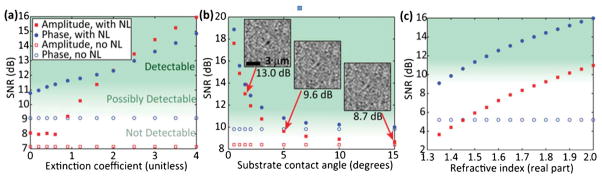
Simulated impact of nanolens improvements on lensfree holographic microscopy. (a) In both amplitude and phase reconstructions, highly absorbing nanolenses around 50 nm particles enhance their contrast with respect to the background. (b) Reducing the contact angle with the substrate makes the nanolenses larger and more effective in detecting 50 nm particles. Insets show amplitude reconstructions for three points in the vicinity of the detection threshold. (c) Nanolenses composed of highly refractive fluids scatter light more effectively, enabling detection of 75 nm particles. All of the amplitude reconstructions without nanolenses in (c) show SNR < 2 dB. For all data in a given subfigure, an identical randomly-generated 1% Gaussian noise field is added at the detector plane. Unless a parameter is being varied explicitly, all simulations assume a purely real film refractive index of 1.35 and a substrate contact angle of 10°. Images adapted from ref. 70.
Acknowledgments
A.O. gratefully acknowledges the support of the Presidential Early Career Award for Scientists and Engineers (PECASE), the Army Research Office (ARO), ARO Young Investigator Award, NSF CAREER Award, ONR Young Investigator Award and the NIH Director’s New Innovator Award DP2OD006427 from the Office of The Director, NIH.
Footnotes
The micro-lenses that are typically employed on opto-electronic sensor-arrays, especially on CMOS designs, do not contribute to image formation and merely improve the external quantum efficiency of each pixel of the sensor-array, and are therefore disregarded in our discussion of lensfree on-chip microscopy.
Notes and references
- 1.Fernández-Suárez M, Ting AY. Nat Rev Mol Cell Biol. 2008;9:929–943. doi: 10.1038/nrm2531. [DOI] [PubMed] [Google Scholar]
- 2.Goldstein M, Naulleau P. Opt Express. 2012;20:15752–15768. doi: 10.1364/OE.20.015752. [DOI] [PubMed] [Google Scholar]
- 3.Cotte Y, Toy F, Jourdain P, Pavillon N, Boss D, Magistretti P, Marquet P, Depeursinge C. Nat Photonics. 2013;7:113–117. [Google Scholar]
- 4.Midgley PA, Weyland M. Ultramicroscopy. 2003;96:413–431. doi: 10.1016/S0304-3991(03)00105-0. [DOI] [PubMed] [Google Scholar]
- 5.Hell SW. Science. 2007;316:1153–1158. doi: 10.1126/science.1137395. [DOI] [PubMed] [Google Scholar]
- 6.Gustafsson MGL, Betzig E, Hess HF, Patterson GH, Lippincott-Schwartz J, Davidson MW. Introduction to Superresolution Microscopy. Carl Zeiss; [accessed Feb. 12, 2013]. http://zeiss-campus.magnet.fsu.edu/articles/superresolution/introduction.html. [Google Scholar]
- 7.Binnig G, Quate C, Gerber C. Phys Rev Lett. 1986;56:930–933. doi: 10.1103/PhysRevLett.56.930. [DOI] [PubMed] [Google Scholar]
- 8.Binnig G, Rohrer H. Helv Phys Acta. 1982;55:726–735. [Google Scholar]
- 9.Lewis A, Isaacson M, Harootunian A, Muray A. Ultramicroscopy. 1984;13:227–231. [Google Scholar]
- 10.Pohl DW, Denk W, Lanz M. Appl Phys Lett. 1984;44:651–653. [Google Scholar]
- 11.Ozcan A, Cubukcu E, Bilenca A, Crozier KB, Bouma BE, Capasso F, Tearney GJ. Nano Lett. 2006;6:2609–2616. doi: 10.1021/nl062110v. [DOI] [PubMed] [Google Scholar]
- 12.Ozcan A, Cubukcu E, Bilenca A, Bouma BE, Capasso F, Tearney GJ. IEEE J Sel Top Quantum Electron. 2007;13:1721–1729. [Google Scholar]
- 13.Gustafsson MGL. J Microsc. 2000;198:82–87. doi: 10.1046/j.1365-2818.2000.00710.x. [DOI] [PubMed] [Google Scholar]
- 14.Gustafsson MGL. Proc Natl Acad Sci U S A. 2005;102:13081–13086. doi: 10.1073/pnas.0406877102. [DOI] [PMC free article] [PubMed] [Google Scholar]
- 15.Keller PJ, Schmidt AD, Santella A, Khairy K, Bao Z, Wittbrodt J, Stelzer EHK. Nat Methods. 2010;7:637–642. doi: 10.1038/nmeth.1476. [DOI] [PMC free article] [PubMed] [Google Scholar]
- 16.Betzig E, Patterson GH, Sougrat R, Lindwasser OW, Olenych S, Bonifacino JS, Davidson MW, Lippincott-Schwartz J, Hess HF. Science. 2006;313:1642–1645. doi: 10.1126/science.1127344. [DOI] [PubMed] [Google Scholar]
- 17.Rust MJ, Bates M, Zhuang X. Nat Methods. 2006;3:793–796. doi: 10.1038/nmeth929. [DOI] [PMC free article] [PubMed] [Google Scholar]
- 18.Hell S, Wichmann J. Opt Lett. 1994;19:780–782. doi: 10.1364/ol.19.000780. [DOI] [PubMed] [Google Scholar]
- 19.Hell SW. Nat Biotechnol. 2003;21:1347–1355. doi: 10.1038/nbt895. [DOI] [PubMed] [Google Scholar]
- 20.Shroff H, Galbraith CG, Galbraith JA, Betzig E. Nat Methods. 2008;5:417–423. doi: 10.1038/nmeth.1202. [DOI] [PMC free article] [PubMed] [Google Scholar]
- 21.Kanchanawong P, Shtengel G, Pasapera AM, Ramko EB, Davidson MW, Hess HF, Waterman CM. Nature. 2010;468:580–584. doi: 10.1038/nature09621. [DOI] [PMC free article] [PubMed] [Google Scholar]
- 22.Frieda KL, Block SM. Science. 2012;338:397–400. doi: 10.1126/science.1225722. [DOI] [PMC free article] [PubMed] [Google Scholar]
- 23.Roth WK, Weber M, Seifried E. Lancet. 1999;353:359–363. doi: 10.1016/S0140-6736(98)06318-1. [DOI] [PubMed] [Google Scholar]
- 24.Matula P, Kumar A, Wörz I, Erfle H, Bartenschlager R, Eils R, Rohr K. Cytometry, Part A. 2009;75A:309–318. doi: 10.1002/cyto.a.20662. [DOI] [PubMed] [Google Scholar]
- 25.Tung YC, Huang NT, Oh BR, Patra B, Pan CC, Qiu T, Chu PK, Zhang W, Kurabayashi K. Lab Chip. 2012;12:3552–3565. doi: 10.1039/c2lc40509a. [DOI] [PMC free article] [PubMed] [Google Scholar]
- 26.Pang L, Chen HM, Freeman LM, Fainman Y. Lab Chip. 2012;12:3543–3551. doi: 10.1039/c2lc40467b. [DOI] [PubMed] [Google Scholar]
- 27.Wu J, Zheng G, Lee LM. Lab Chip. 2012;12:3566–3575. doi: 10.1039/c2lc40517b. [DOI] [PubMed] [Google Scholar]
- 28.Zhu H, Isikman SO, Mudanyali O, Greenbaum A, Ozcan A. Lab Chip. 2013;13:51–67. doi: 10.1039/c2lc40864c. [DOI] [PMC free article] [PubMed] [Google Scholar]
- 29.Zhao Y, Stratton ZS, Guo F, Lapsley MI, Chan CY, Lin SCS, Huang TJ. Lab Chip. 2013;13:17–24. doi: 10.1039/c2lc90127g. [DOI] [PMC free article] [PubMed] [Google Scholar]
- 30.Kim SB, Bae H, Koo K, Dokmeci MR, Ozcan A, Khademhosseini A. J Lab Autom. 2012;17:43–49. doi: 10.1177/2211068211426695. [DOI] [PMC free article] [PubMed] [Google Scholar]
- 31.Isikman SO, Bishara W, Sikora U, Yaglidere O, Yeah J, Ozcan A. Lab Chip. 2011;11:2222–2230. doi: 10.1039/c1lc20127a. [DOI] [PMC free article] [PubMed] [Google Scholar]
- 32.Mudanyali O, Tseng D, Oh C, Isikman SO, Sencan I, Bishara W, Oztoprak C, Seo S, Khademhosseini B, Ozcan A. Lab Chip. 2010;10:1417. doi: 10.1039/c000453g. [DOI] [PMC free article] [PubMed] [Google Scholar]
- 33.Mudanyali O, Oztoprak C, Tseng D, Erlinger A, Ozcan A. Lab Chip. 2010;10:2419–2423. doi: 10.1039/c004829a. [DOI] [PMC free article] [PubMed] [Google Scholar]
- 34.Su TW, Erlinger A, Tseng D, Ozcan A. Anal Chem. 2010;82:8307–8312. doi: 10.1021/ac101845q. [DOI] [PMC free article] [PubMed] [Google Scholar]
- 35.Bishara W, Sikora U, Mudanyali O, Ting-Wei S, Yaglidere O, Luckhart S, Ozcan A. Lab Chip. 2011;11:1276–1279. doi: 10.1039/c0lc00684j. [DOI] [PMC free article] [PubMed] [Google Scholar]
- 36.Greenbaum A, Sikora U, Ozcan A. Lab Chip. 2012;12:1242–1245. doi: 10.1039/c2lc21072j. [DOI] [PubMed] [Google Scholar]
- 37.Lange D, Storment CW, Conley CA, Kovacs GTA. Sens Actuators, B. 2005;107:904–914. [Google Scholar]
- 38.Moon S, Keles HO, Ozcan A, Khademhosseini A, Haeggstrom E, Kuritzkes D, Demirci U. Biosens Bioelectron. 2009;24:3208–3214. doi: 10.1016/j.bios.2009.03.037. [DOI] [PMC free article] [PubMed] [Google Scholar]
- 39.Zheng G, Lee SA, Antebi Y, Elowitz MB, Yang C. PNAS. 2011. [DOI] [PMC free article] [PubMed] [Google Scholar]
- 40.Lee SA, Leitao R, Zheng G, Yang S, Rodriguez A, Yang C. PLoS One. 2011;6:e26127. doi: 10.1371/journal.pone.0026127. [DOI] [PMC free article] [PubMed] [Google Scholar]
- 41.Pang S, Han C, Lee LM, Yang C. Lab Chip. 2011;11:3698–3702. doi: 10.1039/c1lc20654k. [DOI] [PMC free article] [PubMed] [Google Scholar]
- 42.Heng X, Erickson D, Baugh LR, Yaqoob Z, Sternberg PW, Psaltis D, Yang C. Lab Chip. 2006;6:1274–1276. doi: 10.1039/b604676b. [DOI] [PubMed] [Google Scholar]
- 43.Greenbaum A, Luo W, Su TW, Göröcs Z, Xue L, Isikman SO, Coskun AF, Mudanyali O, Ozcan A. Nat Methods. 2012;9:889–895. doi: 10.1038/nmeth.2114. [DOI] [PMC free article] [PubMed] [Google Scholar]
- 44.Isikman SO, Bishara W, Mavandadi S, Yu FW, Feng S, Lau R, Ozcan A. Proc Natl Acad Sci U S A. 2011 doi: 10.1073/pnas.1015638108. [DOI] [PMC free article] [PubMed] [Google Scholar]
- 45.Su TW, Xue L, Ozcan A. Proc Natl Acad Sci U S A. 2012;109:16018–16022. doi: 10.1073/pnas.1212506109. [DOI] [PMC free article] [PubMed] [Google Scholar]
- 46.Garcia-Sucerquia J, Xu W, Jericho SK, Jericho MH, Kreuzer HJ. Optik-International Journal for Light and Electron Optics. 2008;119:419–423. [Google Scholar]
- 47.Balsam J, Ossandon M, Kostov Y, Bruck HA, Rasooly A. Lab Chip. 2011;11:941–949. doi: 10.1039/c0lc00431f. [DOI] [PubMed] [Google Scholar]
- 48.Kim SB, Bae H, Cha JM, Moon SJ, Dokmeci MR, Cropek DM, Khademhosseini A. Lab Chip. 2011;11:1801–1807. doi: 10.1039/c1lc20098d. [DOI] [PMC free article] [PubMed] [Google Scholar]
- 49.Bourquin Y, Reboud J, Wilson R, Zhang Y, Cooper JM. Lab Chip. 2011;11:2725–2730. doi: 10.1039/c1lc20320g. [DOI] [PubMed] [Google Scholar]
- 50.Coskun AF, Sencan I, Su TW, Ozcan A. Opt Express. 2010;18:10510–10523. doi: 10.1364/OE.18.010510. [DOI] [PMC free article] [PubMed] [Google Scholar]
- 51.Coskun AF, Sencan I, Su TW, Ozcan A. PLoS One. 2011;6:e15955. doi: 10.1371/journal.pone.0015955. [DOI] [PMC free article] [PubMed] [Google Scholar]
- 52.Han C, Pang S, Bower DV, Yiu P, Yang C. Anal Chem. 2013;85(4):2356–2360. doi: 10.1021/ac303356v. [DOI] [PMC free article] [PubMed] [Google Scholar]
- 53.Candes EJ, Romberg J, Tao T. IEEE Trans Inf Theory. 2006;52:489–509. [Google Scholar]
- 54.Brady DJ, Choi K, Marks DL, Horisaki R, Lim S. Opt Express. 2009;17:13040–13049. doi: 10.1364/oe.17.013040. [DOI] [PubMed] [Google Scholar]
- 55.Duarte MF, Davenport MA, Takhar D, Laska JN, Sun T, Kelly KF, Baraniuk RG. IEEE Signal Process Mag. 2008;25:83–91. [Google Scholar]
- 56.Shechtman Y, Gazit S, Szameit A, Eldar YC, Segev M. Opt Lett. 2010;35:1148–1150. doi: 10.1364/OL.35.001148. [DOI] [PubMed] [Google Scholar]
- 57.Shechtman Y, Eldar YC, Szameit A, Segev M. Opt Express. 2011;19:14807–14822. doi: 10.1364/OE.19.014807. [DOI] [PubMed] [Google Scholar]
- 58.Szameit A, Shechtman Y, Osherovich E, Bullkich E, Sidorenko P, Dana H, Steiner S, Kley EB, Gazit S, Cohen-Hyams T, Shoham S, Zibulevsky M, Yavneh I, Eldar YC, Cohen O, Segev M. Nat Mater. 2012;11:455–459. doi: 10.1038/nmat3289. [DOI] [PubMed] [Google Scholar]
- 59.Bishara W, Su TW, Coskun AF, Ozcan A. Opt Express. 2010;18:11181–11191. doi: 10.1364/OE.18.011181. [DOI] [PMC free article] [PubMed] [Google Scholar]
- 60.Greenbaum A, Ozcan A. Opt Express. 2012;20:3129–3143. doi: 10.1364/OE.20.003129. [DOI] [PMC free article] [PubMed] [Google Scholar]
- 61.Hardie RC, Barnard KJ, Bognar JG, Armstrong EE, Watson EA. Opt Eng. 1998;37:247–260. [Google Scholar]
- 62.Park SC, Park MK, Kang MG. IEEE Signal Process Mag. 2003;20:21–36. [Google Scholar]
- 63.Elad M, Hel-Or Y. IEEE Trans Image Process. 2001;10:1187–1193. doi: 10.1109/83.935034. [DOI] [PubMed] [Google Scholar]
- 64.Farsiu S, Elad M, Milanfar P. IEEE Trans Image Process. 2006;15:141–159. doi: 10.1109/tip.2005.860336. [DOI] [PubMed] [Google Scholar]
- 65.Isikman SO, Greenbaum A, Luo W, Coskun AF, Ozcan A. PLoS One. 2012;7:e45044. doi: 10.1371/journal.pone.0045044. [DOI] [PMC free article] [PubMed] [Google Scholar]
- 66.Goodman J. Introduction to Fourier Optics. 3. Roberts and Company Publishers; 2004. [Google Scholar]
- 67.Katznelson Y. An Introduction to Harmonic Analysis. 3. Cambridge University Press; 2004. [Google Scholar]
- 68.Ozcan A. PhD Thesis. Stanford University; 2005. p. 17. [Google Scholar]
- 69.Papoulis A. IEEE Trans Circuits Syst. 1975;22:735–742. [Google Scholar]
- 70.Mudanyali O, McLeod E, Luo W, Greenbaum A, Coskun AF, Hennequin Y, Allier CP, Ozcan A. Nat Photon. 2013;7:247–254. doi: 10.1038/nphoton.2012.337. [DOI] [PMC free article] [PubMed] [Google Scholar]
- 71.Eulero L. Methodus Inveniendi Lineas Curvas Maximi Minimive Proprietate Gaudentes (1744) Kessinger Publishing; 2010. [Google Scholar]
- 72.Osserman R. A Survey of Minimal Surfaces. Dover Publications; 1986. [Google Scholar]