Abstract
Ultrafine, uniform nanostructures with excellent functionalities can be formed by self-assembly of block copolymer (BCP) thin films. However, extension of their geometric variability is not straightforward due to their limited thin film morphologies. Here, we report that unusual and spontaneous positioning between host and guest BCP microdomains, even in the absence of H-bond linkages, can create hybridized morphologies that cannot be formed from a neat BCP. Our self-consistent field theory (SCFT) simulation results theoretically support that the precise registration of a spherical BCP microdomain (guest, B-b-C) at the center of a perforated lamellar BCP nanostructure (host, A-b-B) can energetically stabilize the blended morphology. As an exemplary application of the hybrid nanotemplate, a nanoring-type Ge2Sb2Te5 (GST) phase-change memory device with an extremely low switching current is demonstrated. These results suggest the possibility of a new pathway to construct more diverse and complex nanostructures using controlled blending of various BCPs.
For the last several decades, self-assembled block copolymer (BCP) thin films have been extensively studied for applications involving the generation of functional nanostructures1,2,3,4. Moreover, excellent pattern resolution (5 – 20 nm), cost-effectiveness, and scalability of directed self-assembly (DSA) based on BCPs suggest that this is a practical method to complement optical lithography5,6,7,8,9,10,11,12,13,14,15,16,17,18,19. However, extension of the available suite of geometries has been one of the critical challenges in the applications of those functional nanostructures because pure diblock copolymer (di-BCP) thin films present restricted sets of self-assembled morphologies such as spheres, cylinders, gyroids and lamellae12. Various innovative approaches have recently been suggested as potential solutions. For example, non-regular patterns with a wide range of geometric variability were demonstrated using 2-dimensional (2D) dense guiding templates based on electron beam lithography20,21. Novel thin film microdomain structures formed by A-B-C triblock copolymers have also been explored22,23. In addition, BCP double patterning can lead to the formation of hierarchical nanostructures24.
The blending of BCPs has also been widely investigated due to the advantages of simplicity and far more extensive geometric ranges. A rich phase behavior with interesting bulk morphologies was already reported by previous studies25,26,27,28,29,30,31. The governing parameters such as blend composition, volume fraction and molecular weight of each polymer component, and the Flory-Huggins segmental interaction parameter (χ) have also been extensively studied25,27,29. However, the frequent occurrence of macroscopic phase-separation between two di-BCPs often makes it difficult to achieve new and morphologically uniform nanostructures. One general criterion based on the minimization of interfacial energy to ensure uniform microphase separation in blends of A-B and A-C BCPs is that the χ between the B and C (χBC) blocks must be smaller than that between A and B (χAB) and between A and C (χAC), respectively25,26,29. In addition to considerations related to χ, the other key parameters mentioned above also need to be precisely optimized in order to prevent macrophase-separation between constituent BCPs. These strict requirements result in a very narrow process window for the formation of uniform microphase-separated morphologies at the nanoscale27.
In this article, we show how to effectively promote the formation of novel, uniformly microphase-separated thin film morphologies from A-B/B-C BCP blends via host-guest self-assembly mechanism. For example, a hexagonally perforated lamellar (HPL) microdomain (host) formed by an A-B BCP can spontaneously accommodate spherical morphology (guest) made from a B-C BCP, generating ring-shaped nanotemplates. The minimization of free energy by the position-specific incorporation of spherical nano-spheres at the center of the perforations in the HPL structure is theoretically supported by self-consistent field theory (SCFT). Furthermore, we show the formation of a ring-type hollow Ge2Sb2Te5 (GST) phase-change memory device with an extremely low switching current using the blended morphology as a practical nanotemplate.
Results
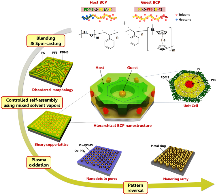
Figure 1 schematically conceptualizes an example of such hybrid nanostructures: hexagonally perforated lamellae (HPL) of one di-BCP (A-b-B) combined with the spherical microdomains of another di-BCP (B-b-C). The compositional choice was designed for the fabrication of nanoscale ring geometries, and the complex nanostructures can be realized by selectively removing the B polymer and reversing the remaining features comprised of the A and C blocks. It should be noted that such complex nanostructures cannot be prepared from a single di-BCP12,32,33. In order to fabricate the designed nanostructures, we chose poly(dimethylsiloxane-b-styrene) (PDMS-b-PS) and poly(styrene-b-ferrocenyldimethylsilane) (PS-b-PFS) di-BCPs, where the pure organic PS (block B) are readily selectively removed and the inorganic-containing PDMS (block A) and PFS (block C) can be oxidized to form robust inorganic nanostructures that can subsequently serve as a high-resolution etch mask as well as a removable template for the formation of functional nanostructures.
Figure 1. Host-guest self-assembly of blended BCPs.
The chemical structures of the PDMS-b-PS and PS-b-PFS diblock copolymers (di-BCPs) used for the self-assembly is shown. The schematics of the as-spun and self-assembled morphologies of the blended BCPs are also presented. A mixed solvent vapor of heptane and toluene induces the formation of a perforated lamellar morphology of PDMS-b-PS that can precisely accommodate the spherical morphology of PS-b-PFS because heptane is selectively segregated in the PDMS blocks, whereas toluene swells PS and PFS blocks more preferentially. An inorganic dots-in-holes nanostructure is produced by oxidation of the hierarchically assembled BCP microdomains. Plasma oxidation selectively removes the PS, while oxidizing PDMS and PFS into stable inorganic materials. The array of metallic nanorings can be obtained from pattern-reversal of the dots-in-holes nanostructure.
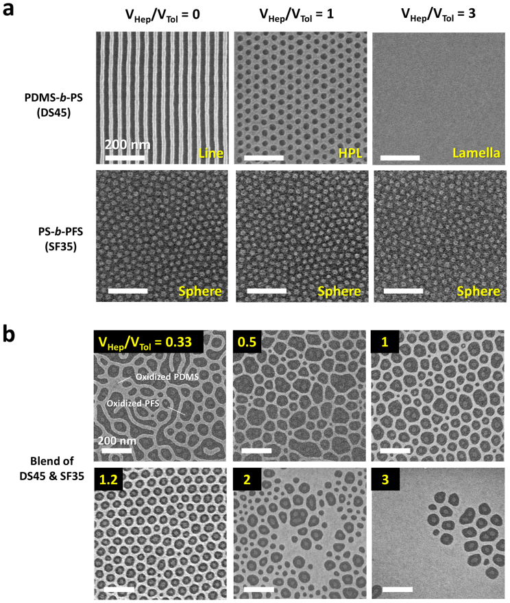
As we demonstrated in our previous study34,35, an unusual degree of geometrical tunability of BCP patterns can be achieved through an annealing treatment with mixed vapors composed of preferentially swelling solvent molecules. For PDMS-b-PS (DS45), with a molecular weight of 45.5 kg/mol and a minority volume fraction of  = 33.7% in the dry state, the sample morphologies showed significant variation depending on the ratio between heptane and toluene used for the solvent-annealing of the BCP, because heptane preferentially swells the PDMS block. Morphological transitions are due to selective swelling of PDMS by heptane and a consequent increase in its effective volume fraction of PDMS (
 ) during solvent annealing34. After the completion of the solvent vapor treatment, the rapid removal of solvent molecules from the BCP samples quenches in-plane morphologies36, due to predominant out-of-plane shrinkage of the film thickness and due to the rise of the effective glass transition temperature (Tg) of the matrix PS block above room temperature. All the solvent vapor treatments in this study were performed at 85°C for accelerated self-assembly37. The morphologies were observed using electron microscopy after subjecting the BCP samples to a two-step sequential CF4 plasma and oxygen plasma treatment process to remove the thin PDMS top layer and PS matrix, respectively38. As shown in Figure 2a, the pure PDMS-b-PS BCP presented cylindrical and HPL morphologies when treated with vapors of pure toluene and a 1:1 mixture of heptane and toluene, respectively. In the HPL (or lamellar catenoid structure)39, the minority block (PDMS) forms a lamellar sheet with well-aligned PS perforations having overall six-fold symmetry. Uniform thru-pores were generated by the removal of the PS domains, as can be seen in the SEM image (Figure 2a, top-middle). The average pore diameter and center-to-center distance were 36 and 58 nm, respectively. In contrast, the morphologies of PS-b-PFS (SF35), with a molecular weight of 35 kg/mol and a minority volume fraction of
  = 11.5%, did not present any noticeable change by varying the fraction of heptane in the treatment vapor, as shown in Figure 2a (bottom). This can be attributed to the small difference in the solubility parameters between PS and PFS40,41, which may induce almost symmetric swelling for the two constituent blocks, thereby preserving the morphology regardless of the treatment conditions. These results on the respective di-BCPs suggest that the effective volume fraction of PDMS (
 ) can be selectively tunable in the blends of PDMS-b-PS and PS-b-PFS via the controlled incorporation of a preferential solvent (heptane).
Figure 2. Self-assembled morphologies of pure BCPs and blended BCPs treated by various mixed solvent vapors.
(a) Morphologies of single-component PDMS-b-PS (DS45) and PS-b-PFS (SF35) in response to different solvent vapors. Cylindrical (top-left), hexagonally perforated lamellar (top-center), and lamellar (top-right) morphologies were obtained from the same PDMS-b-PS BCP by changing the volume ratio of heptane (VHep) and toluene (VTol). PS-b-PFS maintained the same spherical morphology (bottom) for the different solvent vapor treatment conditions. (b) Morphological variation of the BCP blends (PDMS-b-PS and PS-b-PFS) treated by mixed solvent vapors. The BCP blending ratio (VDS45/VSF35) was fixed at 2.5. Uniform host-guest assembly between the two BCPs were achieved at VHep/VTol = 1.2.
As expected, simple mixtures of DS45 and SF35 treated with pure toluene vapor did not present uniformly assembled morphologies in any composition ranges. Based on the solubility parameters of PS (δ = 18.5), PDMS (δ = 15.5), and PFS (δ = 18.6)40,41, the relation χPDMS/PFS ≥ χPDMS/PS
 χPS/PFS is obtained, and thus spatially nonuniform microphase separation occurs due to the strong incompatibility between the two BCPs. Indeed, all the blend samples with a relative mixing ratio of VDS45:VSF35 = 1:1 to 3:1 showed local regions with cylindrical PDMS domains in PS and other regions of spherical PFS domains in PS (as presented in Figure S1), confirming the macrophase separation prediction based on χ parameters. As opposed to the PDMS cylindrical morphology shown in Figure 2a, in the 1:1 blend (Figure S1), the PDMS forms spherical microdomains because of the overall decrease of
  in the blend. As the fraction of DS45 in the blends increases, PDMS microdomains gradually transformed into short cylinders (Figure S1). However, well-ordered microphase-separated morphologies were not obtained for any blending ratio when treated with pure toluene vapor. In addition, thermal annealing also did not induce an ordered morphology of the blend, as shown in Figure S2.
We now demonstrate how mediation by mixed solvent vapors can lead to a new uniform microdomain pattern formed by the host-guest self-assembly of the nominally highly incompatible pair of BCPs. Figure 2b shows how the morphology depends on the volumetric mixture ratio of heptane and toluene (Vhep/Vtol) in the mixed solvent vapors, while the volume ratio of DS45 and SF35 BCPs was fixed at 2.5. With a small amount of heptane added to increase  in the blend, the PDMS cylinders formed a partial network structure (Figure 2b, Vhep/Vtol = 0.33), similar to the mixed morphology of cylinders and perforated lamellae. The expansion of the PDMS block by heptane is supported by a gradual increase of the PDMS area fraction and a decrease of average area per PS perforation with increasing Vhep/Vtol, as shown in Figure 4b. When Vhep/Vtol ~ 0.5, the PDMS network structures became more connected and continuous, and multiple PFS dots were isolated as a group inside the network. Further increase of the heptane fraction resulted in more circular and regular perforations with reduced average diameters, although the variation in the shape and size of the perforations resulted in a variation in the number of PFS spheres per pore.
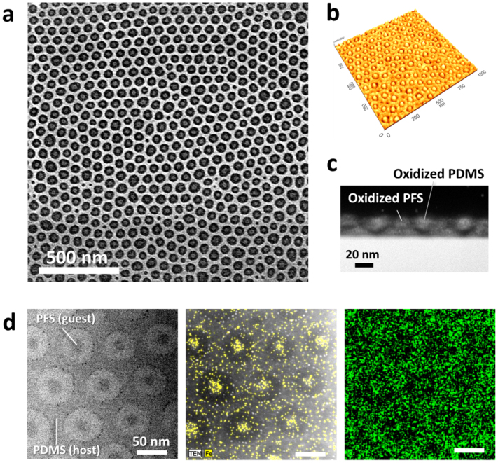
Figure 3. SEM and TEM images of the host-guest self-assembly nanostructures.
(a) A lower-magnification SEM image of the optimized hierarchical morphology. (b) AFM image. (c) – (d) cross-sectional (c) and top-down (d, left) TEM images. EDS elemental mapping results for Fe (d, center) and O (d, right). (d, center) The elemental map is overlapped with a dark field TEM image.
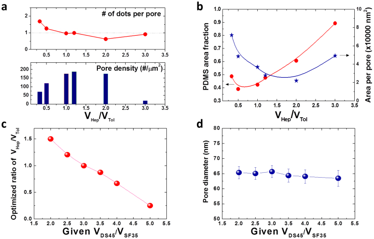
Figure 4. Quantitative measurement data of the BCP blends.
Graphs for the number of dots per pore (a, top) and pore density (a, bottom) and (b) pore area fraction and area per pore at various VHep/VTol ratios. (c) Optimized ratios of VHep/VTol and for diverse VDS45/VFS35 ratios and (d) corresponding pore diameters.
However, further tuning of Vhep/Vtol to approximately 1.2 induced the formation of uniform PS perforations. With the optimized vapor treatment conditions, one-to-one matched host-guest assembly between a PS perforation and a PFS sphere was obtained with maximized pore number density, as presented in Figure 2b (bottom-left), Figure 3a, and Figure 4a. Atomic force microscopy (AFM) and transmission electron microscopy (TEM) images in Figures 3b–3d show the well-defined morphology of the binary BCP blend. Elemental mapping of Fe (Figure 3d, center) and O (Figure 3d, right) confirm that the inner domains are the PFS block. Additional TEM analysis and elemental mapping results are provided in Figures S3 and S4. At the optimized processing conditions, small pores without a central PFS domain were detected at a small fraction (< 4%). Most of the empty pores, with five neighboring pores, were observed at a tilt grain boundary where two pore lattices meet, as shown in Figure S5. This phenomenon is similar to the formation of considerably smaller central cylinders in the case of a pentagonal arrangement compared to a hexagonal arrangement in a cylinder-forming BCP42. This suggests that the spatial constraint imposed on such pores with five neighboring pores may suppress the inclusion of spherical microdomains inside the pores. The removal of the grain boundary and the achievement of long-range ordering using guiding templates are thus expected to eliminate the defects.
It should also be noted that there was a significant increase of pore size and pore-to-pore distance by the incorporation of the spherical PFS microdomains in the PS perforations. The average pore diameter and periodicity with Vhep/Vtol ~ 1.2 were 65 nm and 82 nm, which are 81% and 41% larger, respectively, than the pores of the pure DS45 BCP. The further increase of heptane fraction (Vhep/Vtol ~ 2 – 3) led to the irregular morphologies as shown in Figure 2b (bottom-center and bottom-right). The mixing of a low molecular weight PDMS homopolymer, as presented in Figure S6, also resulted in a similar transformation, despite relatively poor uniformity that likely stems from the less uniform distribution of the homopolymer in the BCP blends compared to the solvent (heptane) molecules. This underscores the critical role of heptane in the highly extensive and effective manipulation of  and the morphological tunability.
The effects of the mixing ratio of DS45 to SF35 BCP while fixing Vhep/Vtol at 1.2 were investigated and are shown in Figure S7. The variations of both VDS45/VSF35 and Vhep/Vtol resulted in similar trends in morphological change, number of PFS dots per pore, pore number density, PDMS area fraction, and area per pore because both VDS45 and Vhep are correlated with  in the blends. The best one-to-one matching between the pores and the dots was obtained at VDS45/VSF35 ~ 2.5 for Vhep/Vtol = 1.2. However, it should be emphasized that the blend mixing composition for uniform formation of the blend morphology is not narrow. Figure 4c and Figure S8 show that Vhep/Vtol can be optimized for different mixing ratios of BCPs (VDS45/VSF35) in a range from 2.0 to 5.0. A clear correlation between the optimum Vhep/Vtol and given VDS45/VSF35 was obtained. The BCP mixture containing less DS45 required more heptane to achieve uniform microphase separation of the blends. The pore size was observed to be independent of the change of VDS45/VSF35, as shown in Figure 4d.
A similar host-guest approach can be taken with blends of PDMS-b-PS and poly(styrene-b-methylmethacrylate) (PS-b-PMMA) for the formation of ring-in-pore structures, as shown in Figure S9. By the selective removal of both the pure organic blocks (PS and PMMA) from the assembled structure, relatively large pores with an average diameter of 56 nm (which is 56% larger compared to that of the simple HPL structure made from a neat PDMS-b-PS) were formed. Figure S10 shows that the blend composed of poly(2-vinylpyridine-b-styrene) (P2VP-b-PS) and PS-b-PFS can form a metallic (Pt) nano-network structure embedded with oxidized PFS dots after the selective incorporation of Pt in the P2VP block and plasma oxidation. These examples demonstrate the promising versatility of host-guest approach for various other BCP combinations.
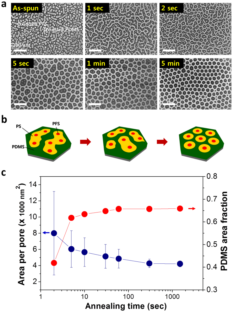
The transformation from the as-cast disordered morphology with separate PDMS and PFS microdomains to an ordered structure clearly occurred with solvent treatment time as shown in Figure 5. The decreased average area per pore and the increased PDMS area fraction during the initial 5 minutes (Figure 5c) suggest that  rises with treatment time. At the very early stage of treatment (1 – 5 sec), the PDMS microdomains merged to form networked structures. With further increase of the treatment time, the number of PFS spheres per pore decreased due to the separation of larger pores into smaller ones (Figure 5a and Figure 5b). The average pore size and number of PFS spheres per pore reached plateaus within 5 minutes of treatment. The spontaneous subdivision of PS perforations and the invariability of the pore size irrespective of the VDS45/VSF35 ratio (Figure 4d) for the optimized Vhep/Vtol imply that the nanostructure is a thermodynamically stable morphology in the solvent annealed state. These results also exclude the possibility that the ordered structure is formed by the accidental trapping of SF35 BCP chains in the PS perforations of DS45.
Figure 5. Time evolution of the self-assembled morphology.
(a) SEM images of samples treated for various annealing times. Due to the use of solvothermal treatment at 85°C, the morphological transition occurred rapidly. (b) Schematic representation of morphological development, showing that the PS pores containing multiple PFS dots are spontaneously split into one-to-one matched microdomain structures. (c) Average pore-area (blue) and PDMS area fraction (red) as a function of annealing time.
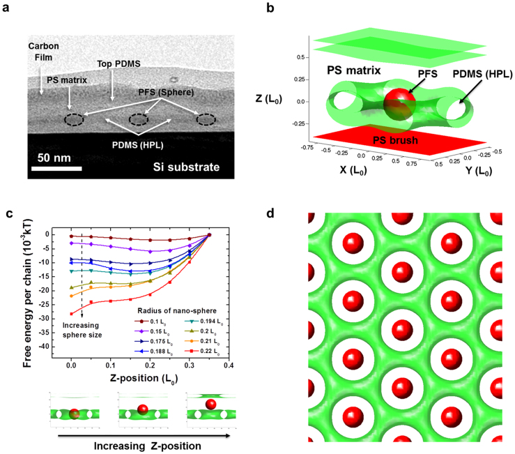
SCFT simulations were utilized to investigate the spontaneous formation of the hybrid nanostructure. We designed our host-guest system by performing simulations of a HPL phase (PDMS-b-PS) and a nano-sphere with a PS shell, which effectively mimics the spherical nature of the PS-b-PFS corona. The unit cell of the hierarchically assembled structure obtained by the simulations was consistent with the cross-sectional TEM image of the sample before plasma oxidation, as seen in Figures 6a and 6b. Previous hybrid-SCFT simulations, employed to study the effects of complex geometries on BCP systems containing defects and nano-spheres [Kim, Y., Chen, H. & Alexander-Katz, A. Unpublished data], revealed that the system is stabilized when a nano-sphere is positioned at a defect center by minimizing the chain stretching of the host BCP. Figure 6c shows the free energy of the perforated lamellar phase of the PDMS-b-PS BCP as a function of the nano-sphere size and the position along the z-axis. For smaller nano-spheres (radius < 0.2 L0), the free energy minimization is achieved when the spheres are located at the junctions (Z ~ ± 0.2 L0) of the PS-lamellar plane and PS-perforation. However, when the radii of the nano-spheres are increased above 0.2 L0, the nano-spheres eventually stabilize the system at the center of the PS-perforations (Z = 0) because larger nano-spheres can reduce PS chain stretching simultaneously at the upper and lower junctions, resulting in the minimum free energy at Z = 0, as shown in Figure 6c. The estimated radius of the PS-b-PFS nano-sphere of the SF35 BCP in the experiment is 0.216 L0 (~17.7 nm), which is consistent with the size that stabilizes the BCP blend system at Z = 0 in the SCFT calculation.
Figure 6. SCFT simulation.
(a) Cross-section TEM image of the host-gest assembled BCP blend. (b) Unit cell structure for the SCFT calculation, which is consistent with the TEM image. (c) Calculated free energy of the PDMS-b-PS HPL morphology depending on the position and size of the guest PS-b-PFS nano-sphere incorporated in the PS perforation. For the particle radius of 0.2 – 0. 22 L0, the minimization of free energy is achieved by the location of nano-sphere at the center. (d) The illustration of periodic configurations achieving the minimum free energy.
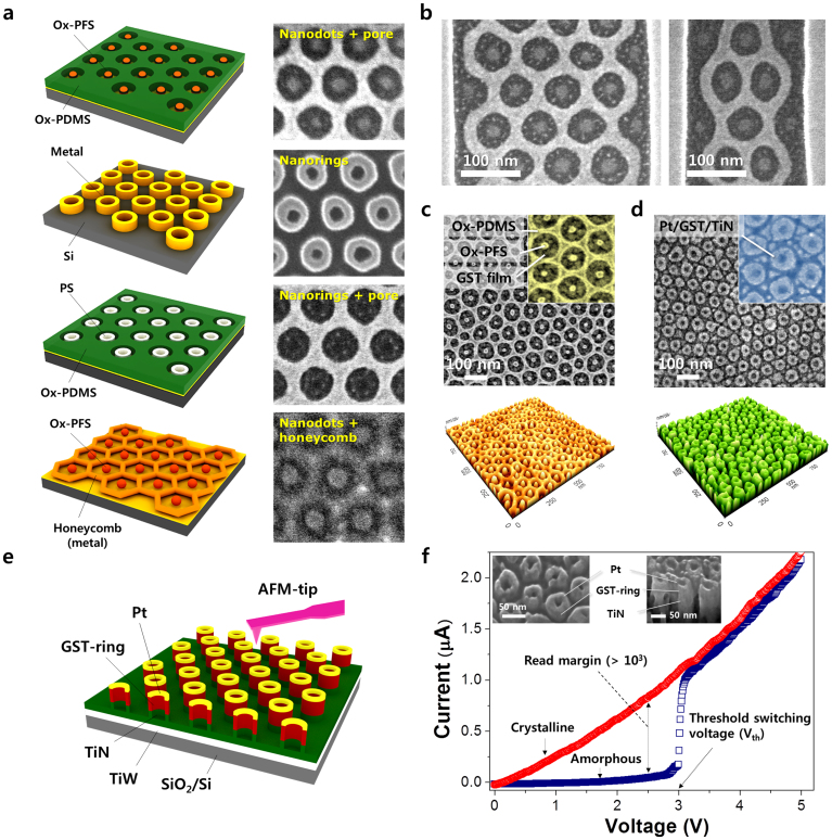
Figure 7a provides a set of the nanoscale geometries that can be obtained through the binary assembly and pattern transfer processes. Structures of dots-in-pores, nanorings, rings-in-pores, and dots-in-honeycomb are demonstrated in Figure 7a with corresponding SEM images. The assembly of these nanostructures can be guided by topographic templates, which control the position and orientation of the microdomain lattice, as presented in Figure 7b. These patterns can also be exploited as useful templates for making functional nanostructures. As an example, Ge2Sb2Te5 (GST) nanorings were fabricated by forming self-assembled structures on GST films (Figure 7c) followed by the use of a Damascene-like pattern reversal process, which was described in detail in Figure S12 and our previous report43. Figure 7d and 7e illustrate a phase-change memory (PCM) cell array with a Pt/GST/TiN nanoring stacking structure with outer and inner diameters of 45 nm and 20 nm, respectively. For measurement of the current-voltage (I-V) characteristics, a conductive atomic force microscope (C-AFM) tip with a radius of 30 nm was used. The results show a clear switching behavior from a high-resistance (amorphous) to a low-resistance (crystalline) state at a threshold voltage of about 3.0 V with a sufficient sensing window (>103 at a read voltage of 2.5 V) (Figure 7f). It is noteworthy that these nanoscale GST rings have a very low switching current of approximately 2 μA, which is close to the lowest programming current ever reported for nanostructures44. This is attributed to the hollow nature combined with the small dimension of the GST nanorings, which significantly shrinks their switching volumes. The nanoring geometry can also be used for the fabrication of multi-bit-storage magnetic memory elements45,46 without relying on high-resolution templates. Moreover, the suboxide nanostructures directly prepared from inorganic-containing BCPs without employing pattern-transfer processes can be applied to high-density resistive memory applications, as we reported previously47. This simple demonstration shows the promise of binary BCP blend nanostructures as useful lithographic templates for the fabrication of ordered functional nanostructures.
Figure 7. Demonstration of pattern transfer and memory device application.
(a) Schematic illustrations and corresponding SEM images of several nanostructures made from the binary BCP self-assembly. Dots-in-pores, nanorings, dots-in-honeycomb, and rings-in-pores are presented. (b) Guided assembly of nanostructure using topographical templates. Because of the affinity of the PS block to the PS brush grafted on the templates, half-cut PS perforations containing PFS spheres align in contact with the side-walls. (c) Self-assembled nanostructures on a GST thin film. (d) Phase-change memory (PCM) nanoring structure fabricated by a metal (Pt) deposition and plasma etch-back process. (e) Schematic illustration of ring-type PCM cell arrays (Pt/GST/TiN/TiW). (f) I-V characteristics of the nanoring PCM structure using C-AFM, showing clear phase-change switching with a very low switching current.
Discussion
The uniform assembly of highly incompatible A-B/B-C di-BCP blends was shown to form useful hybrid nanotemplates by precisely tuning the volume fractions of constituent polymer blocks for controlled insertion of a guest BCP microdomain into a host BCP nanostructure. Our SCFT simulations as well as the experimentally observed morphological evolution of the BCP blends suggest that the position-specific incorporation of the guest microdomain energetically stabilizes the host BCP nanostructure. This methodology is significant in that uniform microphase separation between two BCPs was obtained and it may allow the generation of diverse and complex self-assembly architectures. The host-guest self-assembly combined with pattern reversal enabled the formation of unusual ring-shape nanostructures including hollow phase-change memory nanostructures.
Furthermore, we anticipate the realization of other combinatorial morphologies such as nanoscale line patterns with regularly changing widths or alternatingly occurring dots and line patterns through the one-step binary assembly of various BCPs precisely manipulated by controlled solvent vapor treatment. This will extend the geometry of self-assembled nanostructures. Using the principles revealed through this study, the insertion of inorganic nanoparticles functionalized with proper surfactant molecules at the specific positions of BCP nanostructures can also be suggested as a route to obtain diverse and controlled nanostructures.
Methods
Binary self-assembly of block copolymers
Si substrates were functionalized with a polystyrene (PS) brush by spin-coating 2.5 wt% of a hydroxy-terminated homopolymer (PS-OH, MW = 22 kg/mol). The specimens were then annealed at 150°C for 2 hours in a vacuum oven and washed in toluene to remove remaining homopolymers. All of the BCPs and end-functionalized homopolymers (PDMS-b-PS, PS-b-PFS, and PS-OH were purchased from Polymer Source, Inc. Both PDMS-b-PS (MW = 45.5 kg/mol, fPDMS = 33.7%) and PS-b-PFS (MW = 35 kg/mol, fPFS = 11.5%) BCPs were dissolved at 1.2 wt% in toluene. The two BCP solutions were then mixed at various ratios. The blended BCP solutions were spin-coated onto the PS brush-coated Si substrates and annealed at 85°C for 30 minutes under a mixed vapor of heptane and toluene, which are preferential for PDMS and PS, respectively. The annealed samples were treated with CF4 plasma (20 sec at 50 W) followed by O2 plasma (30 sec at 60 W) using a reactive ion etching (RIE) system, resulting in complete removal of PS, oxidized PDMS and PFS nanostructures. Cross-sectional and top-view TEM samples were prepared by mechanical polishing followed by ion milling with Ar ions. TEM studies were performed using a JEOL JEM-ARM200F microscope with energy dispersive X-ray spectroscopy (EDS) operated at 200 kV.
Fabrication of phase-change nanostructures and measurements
Si wafers with a thermally-grown SiO2 layer (200 nm) were used as substrates. The bottom electrode TiW (150 nm), heater TiN (100 nm), and phase-change material Ge2Sb2Te5 (20 nm) were deposited by radio-frequency (RF) sputtering. Pt was sputter-deposited onto the self-assembled nanostructures and then back-etched by CF4 and Cl2 plasma at 200 W for 2 minutes. To obtain the final GST ring nanostructures, the GST film was patterned using CF4 plasma and Pt nanoring patterns as an etch-mask. The resistive switching behaviors for PCM cell arrays were characterized by using a conductive atomic force microscope (C-AFM, SPA 400, Seiko) with a Pt-coated AFM tip (EFM tips, Nanosensors). While the bottom electrodes (TiW) were grounded, a bias voltage was swept over the top electrode (Pt) from 0 to 5 V with a step size of 0.01 V.
Self-consistent field theory (SCFT) simulations
We simulated the host block copolymer (perforated lamellar phase) and guest block copolymer (nano-sphere attracted to majority block) by utilizing a hybrid particle-field simulation, developed by Fredrickson and co-workers48. To obtain the perforated lamellar phase, the gyroid phase (f = 0.675, χN = 20) of the block copolymer was compressed to thin films with thicknesses comparable to the experiment. The top PDMS brush and bottom PS brush successfully mimicked the experimental PDMS-air interface and Si substrate. To simulate the spherical PS-PFS phase, a nano-sphere with an affinity for the PS blocks and a Gaussian cavity function for the density field of nano-sphere was inserted. Simulations were performed using the newly developed graphics processing unit (GPU) optimized Lattice-Boltzmann diffusion-equation solver49.
Author Contributions
W.I.P. and Y.S.J. conceived the experiments. W.I.P., J.W.J., K.H.K., J.K.Y., Y.H.H. and J.M.K. did the self-assembly experiments. Y.J.K. and A.A. performed the SCFT simulations. W.I.P. fabricated and characterized the phase-change memory nanostructure. W.I.P., Y.S.J., E.L.T., Y.J.K. and A.A. wrote the majority of the paper. All authors contributed to discussions and writing of the paper.
Supplementary Material
Supplementary Information
Acknowledgments
This work was supported by the Center for Integrated Smart Sensors funded by the Ministry of Science, ICT & Future Planning as Global Frontier Project" (CISS-2011-0031848). A. A. acknowledges support by the Center for Excitonics, an Energy Frontier Research Center funded by the U.S. Department of Energy (DOE), Office of Science, Basic Energy Sciences (BES), under Award #DE-SC0001088 (SCFT of block copolymers).
References
- Thurn-Albrecht T. et al. Ultrahigh-Density Nanowire Arrays Grown in Self-Assembled Diblock Copolymer Templates. Science 290, 2126–2129 (2000). [DOI] [PubMed] [Google Scholar]
- Cheng J. Y. et al. Formation of a Cobalt Magnetic Dot Array via Block Copolymer Lithography. Adv. Mater. 13, 1174–1178 (2001). [Google Scholar]
- Warren S. C. et al. Ordered Mesoporous Materials from Metal Nanoparticle–Block Copolymer Self-Assembly. Science 320, 1748–1752 (2008). [DOI] [PubMed] [Google Scholar]
- Zhao Y. et al. Small-molecule-directed nanoparticle assembly towards stimuli-responsive nanocomposites. Nat. Mater. 8, 979–985 (2009). [DOI] [PubMed] [Google Scholar]
- Park M., Harrison C., Chaikin P. M., Register R. A. & Adamson D. H. Block copolymer lithography: Periodic arrays of similar to 1011 holes in 1 square centimeter. Science 276, 1401–1404 (1997). [Google Scholar]
- Segalman R. A., Yokoyama H. & Kramer E. J. Graphoepitaxy of spherical domain block copolymer films. Adv. Mater. 13, 1152–1155 (2001). [Google Scholar]
- Kim S. O. et al. Epitaxial self-assembly of block copolymers on lithographically defined nanopatterned substrates. Nature 424, 411–414 (2003). [DOI] [PubMed] [Google Scholar]
- Cheng J. Y., Mayes A. M. & Ross C. A. Nanostructure engineering by templated self-assembly of block copolymers. Nat. Mater. 3, 823–828 (2004). [DOI] [PubMed] [Google Scholar]
- Cheng J. Y., Ross C. A., Smith H. I. & Thomas E. L. Templated self-assembly of block copolymers: Top-down helps bottom-up. Adv. Mater. 18, 2505–2521 (2006). [Google Scholar]
- Stoykovich M. P. et al. Directed assembly of block copolymer blends into nonregular device-oriented structures. Science 308, 1442–1446 (2005). [DOI] [PubMed] [Google Scholar]
- Chai J., Wang D., Fan X. N. & Buriak J. M. Assembly of aligned linear metallic patterns on silicon. Nat. Nanotechnol. 2, 500–506 (2007). [DOI] [PubMed] [Google Scholar]
- Black C. T. et al. Polymer self assembly in semiconductor microelectronics. IBM Journal of Research and Development 51, 605–633 (2007). [Google Scholar]
- Darling S. B. Directing the self-assembly of block copolymers. Progress in Polymer Science 32, 1152–1204 (2007). [Google Scholar]
- Bita I. et al. Graphoepitaxy of self-assembled block copolymers on two-dimensional periodic patterned templates. Science 321, 939–943 (2008). [DOI] [PubMed] [Google Scholar]
- Ruiz R. et al. Density multiplication and improved lithography by directed block copolymer assembly. Science 321, 936–939 (2008). [DOI] [PubMed] [Google Scholar]
- Jeong S. J. et al. Soft Graphoepitaxy of Block Copolymer Assembly with Disposable Photoresist Confinement. Nano Lett. 9, 2300–2305 (2009). [DOI] [PubMed] [Google Scholar]
- Tavakkoli K. G. A. et al. Templating Three-Dimensional Self-Assembled Structures in Bilayer Block Copolymer Films. Science 336, 1294–1298 (2012). [DOI] [PubMed] [Google Scholar]
- Bates C. M. et al. Polarity-Switching Top Coats Enable Orientation of Sub–10-nm Block Copolymer Domains. Science 338, 775–779 (2012). [DOI] [PubMed] [Google Scholar]
- Jeong J. W. et al. Nanotransfer Printing with sub-10 nm Resolution Realized using Directed Self-Assembly. Adv. Mater. 24, 3526–3531 (2012). [DOI] [PubMed] [Google Scholar]
- Stoykovich M. P. et al. Directed self-assembly of block copolymers for nanolithography: Fabrication of isolated features and essential integrated circuit geometries. ACS Nano 1, 168–175 (2007). [DOI] [PubMed] [Google Scholar]
- Yang J. K. W. et al. Complex self-assembled patterns using sparse commensurate templates with locally varying motifs. Nat. Nanotechnol. 5, 256–260 (2010). [DOI] [PubMed] [Google Scholar]
- Chuang V. P., Gwyther J., Mickiewicz R. A., Manners I. & Ross C. A. Templated Self-Assembly of Square Symmetry Arrays from an ABC Triblock Terpolymer. Nano Lett. 9, 4364–4369 (2009). [DOI] [PubMed] [Google Scholar]
- Chuang V. P., Ross C. A., Bilalis P. & Hadjichristidis N. Nanoscale Rings Fabricated Using Self-Assembled Triblock Terpolymer Templates. ACS Nano 2, 2007–2014 (2008). [DOI] [PubMed] [Google Scholar]
- Son J. G., Hannon A. F., Gotrik K. W., Alexander-Katz A. & Ross C. A. Hierarchical Nanostructures by Sequential Self-Assembly of Styrene-Dimethylsiloxane Block Copolymers of Different Periods. Adv. Mater. 23, 634–639 (2011). [DOI] [PubMed] [Google Scholar]
- Kimishima K., Jinnai H. & Hashimoto T. Control of Self-Assembled Structures in Binary Mixtures of A−B Diblock Copolymer and A−C Diblock Copolymer by Changing the Interaction between B and C Block Chains. Macromolecules 32, 2585–2596 (1999). [Google Scholar]
- Vaidya N. Y. & Han C. D. Temperature−Composition Phase Diagrams for Binary Blends Consisting of Chemically Dissimilar Diblock Copolymers. Macromolecules 33, 3009–3018 (2000). [Google Scholar]
- Frielinghaus H. et al. Blends of AB/BC Diblock Copolymers with a Large Interaction Parameter χ. Macromolecules 34, 4907–4916 (2001). [Google Scholar]
- Asari T., Matsuo S., Takano A. & Matsushita Y. Three-Phase Hierarchical Structures from AB/CD Diblock Copolymer Blends with Complemental Hydrogen Bonding Interaction. Macromolecules 38, 8811–8815 (2005). [Google Scholar]
- Mao H. & Hillmyer M. A. Morphological Behavior of Polystyrene-block-Polylactide/Polystyrene-block-Poly(ethylene oxide) Blends. Macromolecular Chemistry and Physics 209, 1647–1656 (2008). [Google Scholar]
- Tang C. B., Lennon E. M., Fredrickson G. H., Kramer E. J. & Hawker C. J. Evolution of block copolymer lithography to highly ordered square arrays. Science 322, 429–432 (2008). [DOI] [PubMed] [Google Scholar]
- Han S. H., Kim J. K., Pryamitsyn V. & Ganesan V. Phase Behavior of Binary Blends of Block Copolymers Having Hydrogen Bonding. Macromolecules 44, 4970–4976 (2011). [Google Scholar]
- Bates F. S. & Fredrickson G. H. Block Copolymer Thermodynamics - Theory and Experiment. Annual Review of Physical Chemistry 41, 525–557 (1990). [DOI] [PubMed] [Google Scholar]
- Segalman R. A. Patterning with block copolymer thin films. Materials Science & Engineering R-Reports 48, 191–226 (2005). [Google Scholar]
- Jung Y. S. & Ross C. A. Solvent-Vapor-Induced Tunability of Self-Assembled Block Copolymer Patterns. Adv. Mater. 21, 2540–2545 (2009). [Google Scholar]
- Jeong J. W., Park W. I., Kim M.-J., Ross C. A. & Jung Y. S. Highly Tunable Self-Assembled Nanostructures from a Poly(2-vinylpyridine-b-dimethylsiloxane) Block Copolymer. Nano Lett. 11, 4095–4101 (2011). [DOI] [PubMed] [Google Scholar]
- Paik M. Y. et al. Reversible Morphology Control in Block Copolymer Films via Solvent Vapor Processing: An in Situ GISAXS Study. Macromolecules 43, 4253–4260 (2010). [DOI] [PMC free article] [PubMed] [Google Scholar]
- Park W. I. et al. Directed Self-Assembly with Sub-100 Degrees Celsius Processing Temperature, Sub-10 Nanometer Resolution, and Sub-1 Minute Assembly Time. Small 8, 3762–3768 (2012). [DOI] [PubMed] [Google Scholar]
- Jung Y. S. & Ross C. A. Orientation-controlled self-assembled nanolithography using a polystyrene-polydimethylsiloxane block copolymer. Nano Lett. 7, 2046–2050 (2007). [DOI] [PubMed] [Google Scholar]
- Thomas E. L., Anderson D. M., Henkee C. S. & Hoffman D. Periodic area-minimizing surfaces in block copolymers. Nature 334, 598–601 (1988). [Google Scholar]
- Barton A. F. CRC Handbook of Solubility Parameters and Other Cohesion Parameters CRC Press, Boca Raton, FL. (1991). [Google Scholar]
- Wang X. et al. Shell-Cross-Linked Cylindrical Polyisoprene-b-Polyferrocenylsilane (PI-b-PFS) Block Copolymer Micelles: One-Dimensional (1D) Organometallic Nanocylinders. J. Am. Chem. Soc. 129, 5630–5639 (2007). [DOI] [PubMed] [Google Scholar]
- Park C., Yoon J. & Thomas E. L. Enabling nanotechnology with self assembled block copolymer patterns. Polymer 44, 6725–6760 (2003). [Google Scholar]
- Jung Y. S., Lee J. H., Lee J. Y. & Ross C. A. Fabrication of Diverse Metallic Nanowire Arrays Based on Block Copolymer Self-Assembly. Nano Lett. 10, 3722–3726 (2010). [DOI] [PubMed] [Google Scholar]
- Xiong F., Liao A. D., Estrada D. & Pop E. Low-Power Switching of Phase-Change Materials with Carbon Nanotube Electrodes. Science 332, 568–570 (2011). [DOI] [PubMed] [Google Scholar]
- Zhu F. Q. et al. Ultrahigh-Density Arrays of Ferromagnetic Nanorings on Macroscopic Areas. Adv. Mater. 16, 2155–2159 (2004). [Google Scholar]
- Jung Y. S., Jung W. & Ross C. A. Nanofabricated concentric ring structures by templated self-assembly of a diblock copolymer. Nano Lett. 8, 2975–2981 (2008). [DOI] [PubMed] [Google Scholar]
- Park W. I. et al. Self-Assembly-Induced Formation of High-Density Silicon Oxide Memristor Nanostructures on Graphene and Metal Electrodes. Nano Lett. 12, 1235–1240 (2012). [DOI] [PubMed] [Google Scholar]
- Sides S. W., Kim B. J., Kramer E. J. & Fredrickson G. H. Hybrid Particle-Field Simulations of Polymer Nanocomposites. Phys. Rev. Lett. 96, 250601 (2006). [DOI] [PubMed] [Google Scholar]
- Chen H., Kim Y. & Alexander-Katz A. Lattice Boltzmann method for multiscale self-consistent field theory simulations of block copolymers. J. Chem. Phys. 138, 104123 (2013). [DOI] [PubMed] [Google Scholar]
Associated Data
This section collects any data citations, data availability statements, or supplementary materials included in this article.
Supplementary Materials
Supplementary Information


