Abstract
This work describes development of a lab-on-a-chip sensor for electrochemical detection of highly electro-negative heavy metals such as manganese and zinc by anodic stripping voltammetry. The sensor consists of a three-electrode system, with a bismuth working electrode, a Ag/AgCl reference electrode, and a Au auxiliary electrode. Hydrolysis at the auxiliary electrode is a critical challenge in such electrochemical sensors as its onset severely limits the ability to detect electronegative metals. The bismuth working electrode is used due to its comparable negative detection window and reduced toxicity with respect to a conventional mercury electrode. Through optimization of the sensor layout and the working electrode surface, effects of hydrolysis were substantially reduced and the potential window was extended to the −0.3 to −1.9 V range (vs. Ag/AgCl reference electrode), which is far more negative than what is possible with conventional Au, Pt, or carbon electrodes. The described lab-on-a-chip sensor for the first time permits reliable and sensitive detection of the highly electronegative manganese. The favorable performance of the bismuth electrode coupled with its environmentally-friendly nature make the described sensor attractive for applications where disposable chips are desirable. With further development and integrated sample preparation, the lab-on-a-chip may be converted into a point-of-care platform for monitoring heavy metals in blood (e.g., assessment of manganese exposure).
Keywords: Electrochemical sensor, Bismuth electrodes, Anodic stripping voltammetry, Heavy metal detection, Lab-on-a-chip
1 Introduction
Heavy metals are ubiquitous in the environment and have long been recognized to pose significant threat to human health. Blood lead (Pb) concentrations as low as 10 μg/dL have been consistently associated with deficits in IQ and academic achievement (Bellinger et al. 2003; Canfield et al. 2003; Lanphear et al. 2003). Another ubiquitous metal, cadmium (Cd), has the potential to cause kidney, liver, bone, and blood damage (Guallar et al. 2006; Jacquillet et al. 2006; Navas-Acien et al. 2004). Manganese (Mn), although an essential element, is neurotoxic in excess and leads to neurobehavioral dysfunction including deficits in memory, motor function, and may be associated with decreased lung function in occupationally exposed adults (Bellinger et al. 2003; Boojar and Goodarzi 2002; Bowler et al. 2007; Cowan et al. 2009).
Blood is the most reliable parameter for biomonitoring heavy metal exposure (Bader et al. 1999). Whole blood analysis by atomic absorption spectroscopy (AAS) or inductively coupled plasma mass spectroscopy (ICP-MS) are the most common methods for determining heavy metal exposure and assessment of health effects associated with exposure. However, these conventional methods pose numerous challenges. A trained phlebotomist is necessary for collection of blood samples because of the volume required. In most rural high-risk areas, access to a laboratory is limited. Laboratory costs associated with single sample multi-metal measurements are high. Another obstacle is the time delay from sample collection, shipment to a certified metals laboratory and reporting results to families. These challenges impinge the ability to conduct real-time analysis of blood metals to adequately conduct metal exposure assessment.
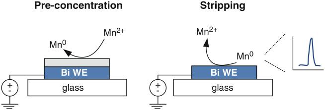
Anodic stripping voltammetry (ASV) is a commonly used electrochemical technique for quantitative analysis of electroactive species such as metals ions. It offers the lowest detection limit of the commonly used electroanalytical techniques, with limits of detection in the picomolar range (Kissinger and Heineman 1996; Krolicka et al. 2003). This sensitivity is due to a pre-concentration step that enormously increases analyte concentration at the electrode surface. The pre-concentrated metal is then analyzed in a separate stripping step that gives a signal proportional to concentration (Fig. 1). In addition to a very low limit of detection, stripping voltammetry requires relatively simple and inexpensive instrumentation, with exceptional suitability for miniaturization. It is these features (and especially the latter) that have stimulated interest in the engineering community to develop microfabricated electrochemical sensors for point-of-care use.
Fig. 1.
Metal determination using two steps of stripping voltammetry on a thin-film bismuth (Bi) working electrode (WE)
This paper describes development of a lab-on-a-chip ASV sensor for point-of-care measurement of highly electronegative metals. The sensor consists of a three-electrode system inside a microfluidic channel. The electrodes include a bismuth (Bi) working electrode, a silver/silver chloride (Ag/AgCl) reference electrode, and a gold auxiliary electrode. Bismuth was selected as the environmentally-friendly electrode material due to its demonstrated suitability for stripping voltammetry, and substantially reduced toxicity as compared with the standard mercury electrode (Jorge et al. 2007; Krolicka et al. 2003; Pauliukaite et al. 2004; Wang et al. 2000). Bismuth electrodes exhibit a high overvoltage for hydrogen evolution resulting in a negative potential window approaching that of a mercury film electrode (Economou and Fielden 2003); none of the conventional electrodes (Au, Pt, or carbon) have sufficiently wide negative potential windows to be used with highly electronegative metals. This negative working window is ideally suited to detect strongly electro-negative metals such as Mn (stripping peak at approximately −1.47 V vs. a 3 MKCl Ag/AgCl reference electrode) and other electronegative metals such as Cd (stripping peak at approximately −0.85 V vs. a 3 MKCl Ag/AgCl reference) and Pb (stripping peak at approximately −0.55 V vs. a 3 M KCl Ag/AgCl reference). On the macroscale, detection of Pb2+, Cd2+, Zn2+, Ti+, In3+, Cu2+, and Sn2+ ions has been demonstrated (Hutton et al. 2006; Kirgöz et al. 2005; Kokkinos et al. 2008; Skogvold et al. 2005; Tarasova 2007; Wang et al. 2001a; Wang et al. 2001b). We envision that development of a portable sensor will lead to improved exposure assessment and will ultimately provide the public health community with the ability to rapidly measure metals in whole blood.
2 Methods
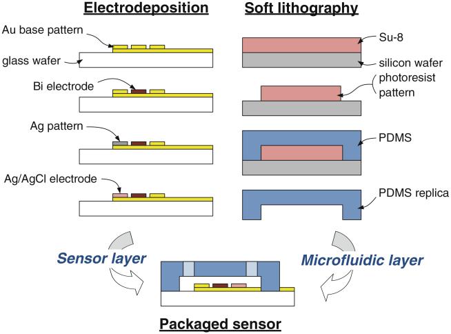
The sensor was fabricated using a combination of electro-deposition and soft lithography techniques. The device fabrication sequence is schematically illustrated in Fig. 2. To fabricate sensor electrodes, metal seed layers (20 nm Ti/200 nm Au) were first deposited by evaporation. The three-electrode pattern with contact pads for electrical connections was formed in the seed layers using photolithography and wet etching. Titanium was etched using a mixture of HNO3: HF: H2O in the 2:1:7 (v/v/v) ratio; Au was etched using a mixture of KI: I2: H2O in the amounts of weight per volume of 20 g: 5 g: 200 ml (w/w/v). The Ag/AgCl reference electrode was fabricated by electrodepositing Ag from a commercial plating solution (Techni-Silver Cyless II RTU, Technic Inc.) using constant current. A cathodic current density of 5 mA/cm2 was applied for 60 s, yielding film thickness of approximately 340 nm. A 1 M KCl solution was used to chloridize the electrodeposited Ag layer with anadic current at 5 mA/cm2 for 30 s. The bismuth working electrode was formed using a solution of 0.1 M acetate buffer (pH 4.65, Sigma Aldrich) and 500 mg/L bismuth (III) in 2% nitric acid solution (Fisher Scientific). Two different deposition methods, namely controlled-current and controlled-potential, were used to fabricate Bi film electrodes. In controlled-current electrodeposition, a constant cathodic current density of 5 mA/cm2 was applied for 4 min using a potentiostat (Reference 600, Gamry). In controlled-potential electrodeposition, a constant potential of −0.8 V was applied for 4 min using a potentiostat (BioAnalytical Systems). The Bi films obtained from the two deposition methods were characterized by SEM and AFM.
Fig. 2.
Microfabrication process diagram. The electrodeposition process involves selective deposition of electrode metals on photolithographically patterned gold seed layer. The soft lithography process involves fabrication of a microfluidic channel in PDMS based on a SU-8 master. The sensor packaging was completed by bonding the PDMS layer on top of the electrode layer using corona discharge
Chip fabrication was completed by bonding a micro-fluidic channel fabricated in polydimethylsiloxane (PDMS) using standard soft lithography methods on top of the fabricated electrodes. An SU-8 negative photoresist (2075, Microchem Corp.) was first used to form a negative master 50 μm deep and 500 μm wide. PDMS monomer (Sylgard 184, Dow Corning) was mixed with curing agent in 10:1 (w/w) ratio. This mixture was degassed for 1 h, cast onto the SU-8 master, and cured on a hot plate at 80°C for approximately 2 h. The cured PDMS replica was peeled from the master and bonded to glass wafer containing the electrode patterns using corona discharge (BD-20, Electro-Technic Products).
Electrochemical performance of the sensors was demonstrated in two ways. First, cyclic voltammetry using a Reference 600 potentiostat was used to characterize the working potential window and onset of hydrolysis. For this, the potential of the working electrode was scanned from −1.8 V to −0.1 V in 0.1 M acetate buffer (pH 5.75) with a scan rate of 75 mV/s. Second ASV detection of heavy metals lead (Pb), cadmium (Cd), and manganese (Mn) was demonstrated. For this, 5 μM metal ion solutions were prepared in 0.1 M acetate buffer (pH 4.65) using metal salts, namely lead (II) acetate trihydrate, cadmium sulfate 8/3-hydrate, and manganese (II) sulfate monohydrate (all ACS grade, ≥99% purity, SigmaAldrich). Metals were pre-concentrated on the working electrode at −1.8 V for 600 s. Following a 15 s resting period, metals were stripped by sweeping the potential positively to −0.4 V using a square wave (25 mV at 15 Hz).
3 Results and discussion
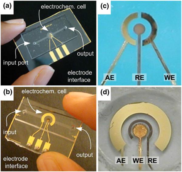
Electrode geometry plays a critical role in electrochemical sensors, and therefore multiple sensor designs incorporating the three electrode cell with different electrode geometries were explored. Photographs illustrating the evolution of the sensor layout from the first to the last design are shown in Fig. 3. In each case the sensor consisted of a three-electrode system, with a Bi working electrode, an Ag/AgCl reference electrode, and an Au auxiliary electrode inside a micro-channel. The desired potential was applied between the working and the reference electrodes. The auxiliary electrode provided the current required to sustain electrolysis at the working electrode. The three electrode system is advantageous because it prevents the reference electrode from driving the current which could change its potential.
Fig. 3.
Photographs of the earlier (a) and the later (b) generation of microfluidic sensor for heavy metal determination. Panels (c) and (d) illustrate close-up images of the sensors. AE auxiliary gold electrode, RE Ag/AgCl reference electrode, WE working Bi electrode
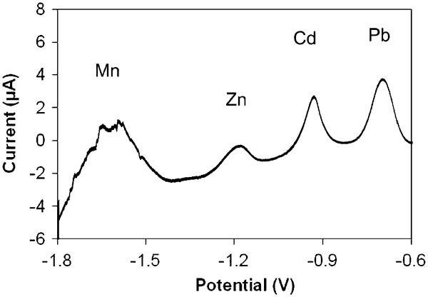
Optimization of electrode geometry with respect to size and layout was especially important since generation of gas bubbles at the Au auxiliary electrode due to electrolysis of water was observed in the first generation sensor when applying negative potentials (<−1.5 V) in attempts to detect highly electronegative metals. Figure 4 shows an anodic stripping voltammogram of our early attempt to simultaneously detect four heavy metals (Mn, Zn, Cd and Pb) contained in a single solution. At the first glance, it appears the sensor is working as four distinct peaks are clearly apparent. However, while the stripping peaks of Cd and Pb are unaffected, the highly electronegative Mn shows heavy influence of solvent electrolysis and the accompanying bubble formation at the auxiliary electrode disrupting the path for charge flow in solution between the auxiliary and working electrodes. This caused the Mn stripping peak to broaden and to be of poor quality, preventing any quantification. In these early experiments, excess gas production resulted in poor sensor stability and reproducibility. Gas bubbles that formed on the auxiliary electrode surface led to surface masking and thus stability issues. Bubbles that dislodged and drifted to the working electrode caused disruptions in metal concentrations near the electrode surface resulting in poor reproducibility. Excessive electrolysis also disrupted the solution connection between the three electrodes in the small channel of the microfluidics system, causing high resistance and loss of potential control of the working electrode giving erratic behavior of the sensor system. In a number of severe cases, loss of the auxiliary electrode was observed due to excessive and aggressive bubble formation that caused Au film adhesion loss and flaking.
Fig. 4.
ASV measurement of Mn, Zn, Cd and Pb at concentrations of approximately 20 μM, 15 μM, 9 μM, 5 μM, respectively. Analytes were pre-concentrated at −1.8 V for 600 s on an electrodeposited bismuth working electrode of the earlier sensor design
The conventional strategy for minimizing hydrolysis is to limit the potential scan to above −1.5 V, which minimizes the current in the sensor and the amount of electrolysis at the auxiliary electrode. However, this approach is not suitable for detection of highly electronegative metals such as Mn, which strips at approximately −1.47 V (vs. 3 M KCl Ag/AgCl), as the potential must be much more negative during the metal pre-concentration step. Our most successful strategy was to increase the area of the auxiliary electrode and the distance between the working and the auxiliary electrodes. This is clearly evident from Fig. 3, which illustrates the final design with a 20× larger auxiliary electrode area from the initial design (10 mm2 vs. 0.5 mm2). Increasing the area of the auxiliary electrode while maintaining the area of the working electrode reduced the current density required to sustain the electrochemical reaction at the auxiliary electrode. In essence, while the same gas production occurred, the larger area made the gas bubbles less concentrated and therefore reduced their effect on the sensor. The distance between the working and auxiliary electrode was increased from 400 μm in the earlier designs to 1.65 mm for the final design. By increasing the distance between the auxiliary and working electrode, less interference due to gas production was observed due to the increased distance the bubbles must traverse to affect the working electrode.
A stable reference electrode is an important component of an integrated electrochemical system and is a prerequisite for achieving reliable performance. The key advantages of using Ag/AgCl reference electrodes are the desirable electrochemical characteristics and process compatibility. The Ag/AgCl electrode is based on a very high exchange-current density reaction, which means that at low current densities the electrode is not polarized and the potential at the electrode/electrolyte interface is a function of Cl− activity only. One factor known to limit stability of the Ag/AgCl electrodes is the well-known solubility of AgCl in solutions. This problem, although trivial for millimeter scale electrodes, can become critical for thin-film electrodes where only a few hundred nanometers of AgCl are present. This problem was overcome by depositing a relatively thick 350 nm layer of silver chloride. We found this thickness to be sufficient for repeated sensor operation over a 1-week period (over 4 h of continuous operation). For longer lifetimes, thicker layers of Ag and AgCl can be deposited if necessary (thicknesses exceeding 1 μm have been reported (Bousse et al. 1986)).
The working electrode plays an essential role in ASV sensors because this is where the metals are detected by pre-concentration and stripping. In this work, bismuth was used as the working electrode material due to its demonstrated suitability for stripping voltammetry of electronegative metals and substantially reduced toxicity over the standard mercury electrode (Jorge et al. 2007; Krolicka et al. 2003; Pauliukaite et al. 2004; Wang et al. 2000). The working potential window of bismuth is limited by the potential required for oxidation of Bi0 to Bi3+, which leads to an upper limit for the bismuth electrode of approximately −0.3 V. On the negative side, the potential window is flanked by the onset of hydrolysis, at approximately −1.7 V. This negative working potential window is ideally suited to detect strongly electronegative metals such as Mn and Zn (stripping peak at approximately −1.35 V), as well as other electronegative metals such as Cd (stripping peak at approximately −0.85 V) and Pb (stripping peak at approximately −0.55 V). An added benefit of using bismuth is that its films can be electro-deposited on a number of conductive surfaces, making it compatible with standard lab-on-a-chip fabrication methods. The low toxicity of bismuth allows for the development of environmentally-friendly disposable devices(Rodilla et al. 1998; Sun et al. 1999), which can be utilized for a variety of point-of-care applications.
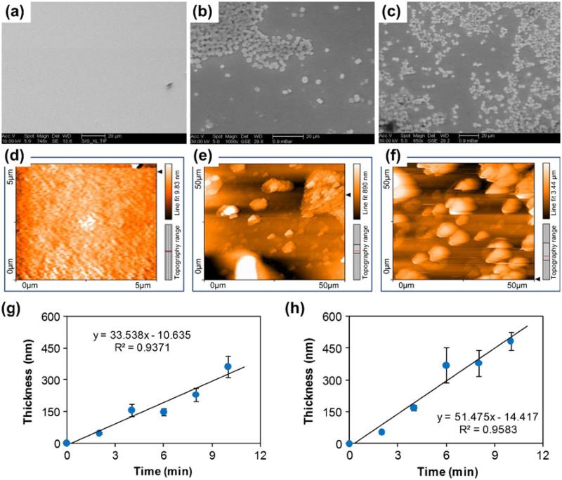
In stripping analysis, the working electrode surface plays a critical role as it influences the ability of the analyte to be stripped and therefore detected. Thus, working electrode surface roughness (or rather surface smoothness) is important and was investigated. We compared controlled-current and controlled-potential methods of Bi deposition and found the latter to be the better procedure for preparing the electrode. A controlled −0.8 V potential worked best as compared to the controlled current at 5 mA/cm2 for 4 min of Bi film deposition. Figure 5 compares the surfaces of the deposited Bi using the two methods with a plain Au surface. During electrodeposition, a Bi film covers the Au seed layer first and then starts to grow grain clusters. AFM analysis indicated that the formation of the grain clusters was much more dense for the controlled potential–deposition, with surface roughness of εRMS ~ 230 ± 49 nm, as compared with the controlled-current condition at 5 mA/cm2 (εRMS ~ 610 ± 78 nm). The current density increased constantly during the controlled potential deposition and was often higher than the current density used for the controlled-current deposition. Thus the controlled-potential method not only had increased surface roughness and thus overall surface area, but also exhibited the ability to deposit thicker films for the time intervals selected. An electrode-position rate of ~51 nm/min for the controlled-potential (vs. ~34 nm/min for the controlled-current condition) was measured for the Bi electrodeposition cell (Fig. 5(g–h)), which offers excellent control of the deposited film thickness.
Fig. 5.
Comparison of Bi films electrodeposited by controlled-current (5 mA/cm2) and controlled-potential (−0.8 V). SEM images of the (a) Au seed layer, (b) controlled current Bi film, and c controlled potential Bi film illustrate surface quality. AFM scans of the (d) Au seed layer, (e) controlled current Bi film, and (f) controlled potential Bi film illustrate surface roughness. Controlled current electrodeposition method exhibited a lower film deposition rate (g) as compared with the controlled potential condition (h). Film thickness was measured over a 1 cm2 area using profilometery
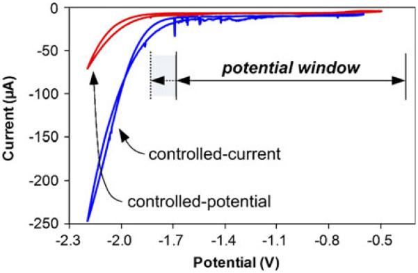
Ultimately, the surface properties of the working electrode affect the working potential window of the electrochemical sensor and the onset of hydrolysis. Cyclic voltammograms of Bi films deposited by the controlled-current and controlled-potential methods in acetate buffer (pH 5.75) are compared in Fig. 6. The Bi film formed by controlled-current exhibited extensive hydrolysis with a potential window ranging from −1.7 V to −0.3 V. The hydrolysis was reduced substantially when the Bi electrode was formed by controlled-potential, with a much wider negative potential window ranging from −1.9 V to −0.3 V. This is a critically important result for detection of highly electronegative metals, as the favorable shift of the hydrolysis away from the detection region reduces the background noise. Thus, owing to the larger surface area and the wider potential window of the potential-controlled Bi film, the measured peak currents of the anodic stripping analysis proved to be higher, with sharper and smoother stripping peaks. Thus, the controlled-potential method of Bi deposition is clearly superior and was selected for the results presented herein.
Fig. 6.
Cyclic voltammetry comparison of the working potential windows of the Bi working electrodes prepared by controlled-current (5 mA/cm2) and controlled-potential (−0.8 V). Dotted lines indicate extension of the working potential window for the Bi film prepared by controlled-potential deposition. Both results are in 0.1 M sodium acetate pH 5.75 buffer, with a scan rate of 75 mV/s; all potentials vs. Ag/AgCl reference electrode
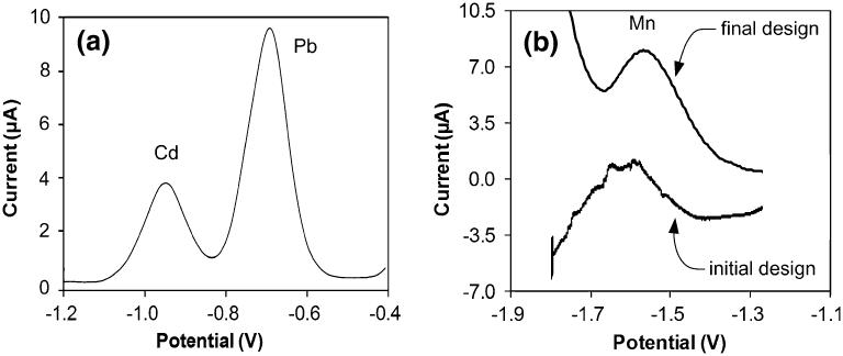
The final sensor design exhibited a much improved detection capability, as illustrated by results presented in Fig. 7. The voltammogram in Fig. 7(a) was the measurement obtained from a solution containing both Pb and Cd ions. At first glance, the stripping waveforms of Cd (9 μM) and Pb (5 μM) appear to be the same as the results obtained with the earlier sensor design in Fig. 4. However, the measured peak currents and quality have improved. Specifically, for the same metal concentration in the sample and 600 s pre-concentration time, the peak current for Pb increased tenfold from ~3.35 μA in the earlier design to ~9 μA, while the peak full width at half maximum (FWHM) remained the same ~88 mV. Similarly, the stripping waveform for Cd increased in amplitude from ~2.39 μA to ~4 μA for a 9 μM sample (a ~2× increase in signal for the same concentration), while the peak FWHM increased slightly from ~73 mV to ~100 mV.
Fig. 7.
Measurements of metal ions with the final sensor design. (a) ASV waveforms illustrating measurement of Cd (9 μM) and Pb (5 μM) metals. (b) Comparison of ASV waveforms for measurement of Mn with the final and initial designs. Metal concentrations were 5 μM and 20 μM, respectively. All analytes were pre-concentrated at −1.8 V for 600 s on an electro-deposited bismuth working electrode
Most importantly, however, the stripping waveform of Mn showed a remarkable improvement. Figure 7(b) compares the stripping peaks we obtained with our initial and final designs at similar Mn concentrations (20 μM vs. 5 μM). The most obvious improvement is the smooth, noise-free shape of the peak measured with the final design, which can now be quantified. Another distinct improvement is the amplitude of the current change—in the initial design the waveform shows a ~5 μA current change for the 20 μMMn sample, while the final design yields a ~5 μA stripping peak but for the 5 μMMn sample. The peaks became sharper as well, with the FWHM decreasing from ~228 mV in the initial design to ~145 mV in the final design. From these results it is clear that the final sensor design is capable of detecting highly electronegative metals such as Mn and offers superior measurement capabilities for even mildly electronegative metals such as Pb and Cd. These results also show the sensor is capable of multi-analyte detection in the low μM concentration range, which is the relevant range for assessment of heavy metal exposure in physiological samples such as blood or urine (in a healthy adult blood levels of Pb, Zn and Mn are typicall at or below 20 μg/dL (1 μM), 90 μg/dL (18 μM), and 50 μg/L (1 μM), respectively(Ellingsen et al. 2006; Goullé et al. 2005; Hotz et al. 2003)).
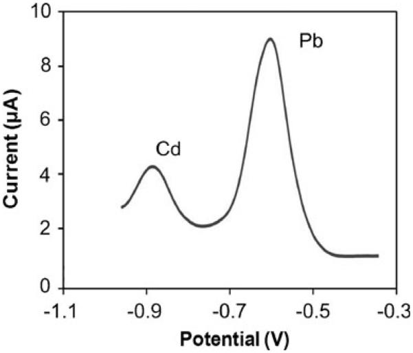
To demonstrate the ability of the sensor to measure metals in biological samples, Pb and Cd were measured in blood serum. For this, blood was drawn from a healthy adult male into a metal free, sterile, Royal Blue Top tube (BD Vacutainer) and centrifuged (Eppendorf 5810R) at 4,000 rpm for 8 min at 35 C. Serum was taken off with a pipette into a tube, diluted in a 1:5 ratio with 100 mM sodium acetate buffer (pH 5.75), and spiked with 5 μM of Pb and 9 μM of Cd. Figure 8 shows a representative voltammogram, illustrating the stripping peaks for both metals. The peaks shifted slightly in potential, approximately +100 mV, which is attributed to the increased Cl− concentration in the serum sample. It is important to note that the stripping peaks in serum samples yielded peak currents comparable to the peak currents obtained in buffer only (Fig. 7(a)), although the background was slightly higher. This difference in background could be due a number of factors, including biofouling of the bismuth electrode (as some protein deposition was observed at the working electrode). Nevertheless, the initial 3~5 measurements with each sensor yielded reproducible results, which is more than adequate for disposable devices. If sensor operation for a longer period is necessary, strategies will need to be developed to address biofouling. One possible approach that has proven to be successful is to coat electrodes with a Nafion film, which is permeable to metal ions (Hurst and Bruland 2005).
Fig. 8.
ASV waveform illustrating measurement of Cd (9 μM) and Pb (5 μM) metals in blood serum. The sample was diluted with 0.1 M sodium acetate buffer (pH 5.75) in 1:5 ratio. Analytes were pre-concentrated at −1.8 V for 600 s on an electrodeposited bismuth working electrode
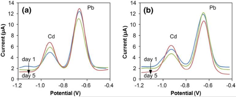
The sensor exhibited high reproducibility over multiple days, with hours of continuous operation. The measurement reported in Fig. 7(a) is an average from three separate experiments on the same sample, with the standard deviations of 1.36 μA and 0.47 μA for Pb and Cd respectively. Similarly smallvariabilitywasobserved in blood serum, with an average from four separate experiments on the same sample exhibiting standard deviations of 1.72 μA and 0.34 μA for Pb and Cd respectively (Fig. 8). To further assess reproducibility, multiple sensors were used to perform repeated measurements of 5 μM Pb and 9 μM Cd in 0.1 M sodium acetate buffer (pH 5.75) over a 5 day period (n=24). Following each measurement, sensors were rinsed with DI water, blow-dried with nitrogen, and stored in ambient air until then next measurement. Representative results are shown in Fig. 9 (for clarity, data for only two sensors for days 1, 3, and 5 are shown). The mean peak currents for each metal were 9.6 μA for Pb and 3.6 μA for Cd, with standard deviations of 1.37 μA and 1.26 μA respectively. Continued sensor use beyond 5 days, up to 36 sequential measurements, resulted in signal drift and ultimately sensor failure, most commonly due to the eventual loss of the auxiliary electrode to hydrolysis. Nevertheless, considering that the sensor is ultimately intended to be disposable, failure after repeated use is not a performance issue. Overall, these results indicate that sensors performed consistently, regardless of being used immediately following fabrication or being stored prior to or between measurements.
Fig. 9.
Representative results of repeated measurements of Cd (9 μM) and Pb (5 μM) metals in sodium acetate buffer over a 5 day period by two different sensors. Between measurements sensors were cleaned and stored in ambient air. All analytes were pre-concentrated at −1.8 V for 600 s; for clarity only data for two sensors on days 1, 3, and 5 are presented
The described sensor is the first lab-on-a-chip capable of measuring highly electronegative Mn, and its design has several distinct advantages. First, the modifications in the configuration of the electrodes delayed the onset of hydrolysis and permitted detection of highly electronegative metals. The quality of the stripping peaks improved, with stripping waveforms exhibiting increase in peak current, peak sharpness, and elimination of peak noise due to hydrolysis. Second, the bismuth electrodes offer an environmentally-friendly solution to the conventionally used mercury electrode. The other commonly used electrodes such as Au, Pt and carbon do not have sufficiently wide negative potential windows to be used with Mn and other highly electronegative metals. Third, electrodepositing bismuth in situ (inside microfluidic chip) offers a renewed fresh sensing surface for repeated analyses or for multi-metal analysis. This also increases reliability and repeatability of the sensor for repeated analyses as well as the durability and lifetime of the sensor increased as Bi films can be reproduced repeatedly.
4 Conclusions
The developed lab-on-a-chip demonstrates suitability of bismuth electrodes for stripping voltammetry measurement of highly electronegative metals such as manganese. The electrode configuration and working electrode surface have been optimized in order to minimize hydrolysis and extend the working potential window down to −1.9 V. The hydrolysis problem was solved by increasing the auxiliaryelectrode area and by placing the auxiliaryelectrode further away from the bismuth working electrode. Comparing ASV measurements of the initial and final designs convincingly demonstrate that the film quality of the working electrode, the optimum area of the electrodes, and the layout of the three-electrode system play an important role for successful measurement and detection of analyte ions in sample solutions. The favorable performance of the bismuth electrode coupled with its environmentally-friendly nature make the described electrochemical sensor extremely attractive for on-site and point-of-care measurements. Ultimately, we expect reductions in sample size (drops of blood from a single lancet puncture as opposed to blood draw) and integration of sample preparation (dilution and mixing steps) onto the chip to make it user-friendly. With further developments, the chip may be converted into a self-check mechanism, such as with glucose screening for diabetics.
Acknowledgements
This work was supported by a grant from the National Institute of Environmental Health Sciences (NIEHS), Grant Number R21ES019255, and the National Institute of Occupational Safety and Health (NIOSH) Pilot Research Project Training Program at the University of Cincinnati (T42OH008432).
References
- Bader M, Dietz MC, Ihrig A, Triebig G. Int. Arch. Occup. Environ. Health. 1999;72:521. doi: 10.1007/s004200050410. [DOI] [PubMed] [Google Scholar]
- Bellinger DC, Needleman HL, Eden AN, Donohoe MT, Canfield RL, Henderson CR, Jr., Lanphear BP. N. Engl. J. Med. 2003;349:500. [Google Scholar]
- Boojar MMA, Goodarzi F. J. Occup. Environ. Med. 2002;44:282. doi: 10.1097/00043764-200203000-00016. [DOI] [PubMed] [Google Scholar]
- Bousse LJ, Bergveld P, Geeraedts HJM. Sens. Actuators. 1986;9:179. [Google Scholar]
- Bowler RM, Roels HA, Nakagawa S, Drezgic M, Diamond E, Park R, Koller W, Bowler RP, Mergler D, Bouchard M, Smith D, Gwiazda R, Doty RL. Occup. Environ. Med. 2007;64:167. doi: 10.1136/oem.2006.028761. [DOI] [PMC free article] [PubMed] [Google Scholar]
- Canfield RL, Henderson CR, Jr., Cory-Slechta DA, Cox C, Jusko TA, Lanphear BP. N. Engl. J. Med. 2003;348:1517. doi: 10.1056/NEJMoa022848. [DOI] [PMC free article] [PubMed] [Google Scholar]
- Cowan DM, Zheng W, Zou Y, Shi X, Chen J, Rosenthal FS, Fan Q. Neurotoxicology. 2009;30:1214. doi: 10.1016/j.neuro.2009.02.005. [DOI] [PMC free article] [PubMed] [Google Scholar]
- Economou A, Fielden PR. Analyst. 2003;128:205. [PubMed] [Google Scholar]
- Ellingsen DG, Dubeikovskaya L, Dahl K, Chashchin M, Chashchin V, Zibarev E, Thomassen Y. J. Environ. Monit. 2006;8:1078. doi: 10.1039/b605549d. [DOI] [PubMed] [Google Scholar]
- Goullé J, Mahieu L, Castermant J, Neveu N, Bonneau L, Lainé G, Bouige D, Lacroix C. Forensic Sci. Int. 2005;153:39. doi: 10.1016/j.forsciint.2005.04.020. [DOI] [PubMed] [Google Scholar]
- Guallar E, Silbergeld EK, Navas-Acien A, Malhotra S, Astor BC, Sharrett AR, Schwartz BS. Am. J. Epidemiol. 2006;163:700. doi: 10.1093/aje/kwj090. [DOI] [PubMed] [Google Scholar]
- Hotz C, Peerson JM, Brown KH. Am. J. Clin. Nutr. 2003;78:756. doi: 10.1093/ajcn/78.4.756. [DOI] [PubMed] [Google Scholar]
- Hurst MP, Bruland KW. Anal. Chim. Acta. 2005;546:68–78. doi: 10.1016/j.aca.2005.05.015. [DOI] [PubMed] [Google Scholar]
- Hutton EA, Hočevar SB, Mauko L, Ogorevc B. Anal. Chim. Acta. 2006;580:244. doi: 10.1016/j.aca.2006.07.075. [DOI] [PubMed] [Google Scholar]
- Jacquillet G, Barbier O, Cougnon M, Tauc M, Namorado MC, Martin D, Reyes JL, Poujeol P. American Journal of Physiology—Renal Physiology. 2006:290. doi: 10.1152/ajprenal.00366.2004. [DOI] [PubMed] [Google Scholar]
- Jorge EO, Neto MMM, Rocha MM. Talanta. 2007;72:1392. doi: 10.1016/j.talanta.2007.01.047. [DOI] [PubMed] [Google Scholar]
- Kirgöz UA, Marín S, Pumera M, Merkoçi A, Alegret S. Electroanalysis. 2005;17:881. [Google Scholar]
- Kissinger P, Heineman WR. Laboratory Techniques in Electroanalytical Chemistry. 1996:1008. [Google Scholar]
- Kokkinos C, Economou A, Raptis I, Efstathiou CE. Electrochim. Acta. 2008;53:5294. [Google Scholar]
- Krolicka A, Bobrowski A, Kalcher K, Mocak J, Svancara I, Vytras K. Electroanalysis. 2003;15:1859. [Google Scholar]
- Lanphear BP, Dietrich KN, Berger O. Ambul. Pediatr. 2003;3:27. doi: 10.1367/1539-4409(2003)003<0027:poltiu>2.0.co;2. [DOI] [PubMed] [Google Scholar]
- Navas-Acien A, Selvin E, Sharrett AR, Calderon-Aranda E, Silbergeld E, Guallar E. Circulation. 2004;109:3196. doi: 10.1161/01.CIR.0000130848.18636.B2. [DOI] [PubMed] [Google Scholar]
- Pauliukaite R, Hočevar SB, Ogorevc B, Wang J. Electroanalysis. 2004;16:719. [Google Scholar]
- Rodilla V, Miles AT, Jenner W, Hawksworth GM. Chem. Biol. Interact. 1998;115:71. doi: 10.1016/s0009-2797(98)00059-3. [DOI] [PubMed] [Google Scholar]
- Skogvold SM, Mikkelsen Ø, Schrøder KH. Electroanalysis. 2005;17:1938. [Google Scholar]
- Sun H, Li H, Harvey I, Sadler PJ. J. Biol. Chem. 1999;274:29094. doi: 10.1074/jbc.274.41.29094. [DOI] [PubMed] [Google Scholar]
- Tarasova VA. J. Anal. Chem. 2007;62:157. [Google Scholar]
- Wang J, Lu J, Hočevar SB, Farias PAM, Ogorevc B. Anal. Chem. 2000;72:3218. doi: 10.1021/ac000108x. [DOI] [PubMed] [Google Scholar]
- Wang J, Hočevar SB, Deo RP, Ogorevc B. Electrochem. Commun. 2001a;3:352. [Google Scholar]
- Wang J, Lu J, Hočevar SB, Ogorevc B. Electroanalysis. 2001b;13:13. [Google Scholar]


