Abstract
The adoption of solid state photo-detectors for positron emission tomography (PET) system design and the interest in 3D interaction information from PET detectors has lead to an increasing number of readout channels in PET systems. To handle these additional readout channels, PET readout electronics should be simplified to reduce the power consumption, cost, and size of the electronics for a single channel. Pulse width modulation (PWM), where detector pulses are converted to digital pulses with width proportional to the detected photon energy, promises to simplify PET readout by converting the signals to digital form at the beginning of the processing chain, and allowing a single time-to-digital converter to perform the data acquisition for many channels rather than routing many analog channels and digitizing in the back end. Integrator based PWM systems, also known as charge-to-time converters (QTC), are especially compact, reducing the front-end electronics to an op-amp integrator with a resistor discharge, and a comparator. QTCs, however, have a long dead-time during which dark count noise is integrated, reducing the output signal to noise ratio. This work presents a QTC based PWM circuit with a gated integrator that shows performance improvements over existing QTC based PWM. By opening and closing an analog switch on the input of the integrator, the circuit can be controlled to integrate only the portions of the signal with a high signal-to-noise ratio. It also allows for multiplexing different detectors into the same PWM circuit while avoiding uncorrelated noise propagation between photodetector channels. Four gated integrator PWM circuits were built to readout the spatial channels of two position sensitive solid state photomultiplier (PS-SSPM). Results show a 4×4 array 0.9mm×0.9mm×15mm of LYSO crystals being identified on the 5mm×5mm PS-SSPM at room temperature with no degradation for 2-fold multiplexing. In principle, much larger multiplexing ratios are possible, limited only by count rate issues.
1. Introduction
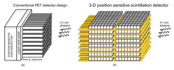
High resolution PET scanners readout many small scintillation crystals. Many systems use some form of light sharing to reduce the number of readout channels needed. However, with the advent of solid-state detectors, PET scanners are moving towards increasingly more readout channels. 3-D positioning PET detectors, which have the capability to directly measure the individual interaction coordinates of multiinteraction photon events, will further improve the performance of high resolution PET (Levin et al. 2012), but require many more readout channels (e.g. Fig. 1). To readout all the channels the electronics must be extremely compact to fit in a densely packed detector geometry, and low power to avoid heating the temperature sensitive solid-state detectors (Vandenbroucke et al. 2012), (Schmall et al. 2012). However, as readout channels correspond to ever smaller crystal volumes, the fact that each readout channel sees a low count rate can be used to multiplex the readout electronics and share the analog-to-digital converter. If a method is found to more simply and compactly readout PET detectors, high channel count PET systems can be created, enabling new PET capabilities.
Figure 1.
(a) A traditional PET detector block with 4 readout channels and light multiplexing. One such block, used in the Siemens Inveon, reads 10240mm3 LSO (2560mm3 per channel) (Mintzer et al. 2007). (b) The proposed 3-D position sensitive PET detector block has 80 readout channels, and reads 1600mm3 LSO (20mm3 per channel). The methods proposed in this paper would reduce the readout of this detector block to 5 channels or 320mm3 LSO per channel.
If the photodetector pulse is sent to a comparator, the time over a threshold (TOT) will be related to the energy of the photon detected. This digital pulse can then be easily multiplexed and read FPGA based time-to-digital converters (Hong et al. 2012). However, the TOT relationship is non-linear, reducing the energy and the position resolution in position sensitive detectors. Various techniques have been proposed to correct this non-linearity including multiple thresholds (Fujiwara et al. 2010), dynamic thresholds (Shimazoe et al. 2010), and pulse-width modulation (PWM) using peak detection (Olcott et al. 2008) or integrator charge-to-time converters (QTC) (Streun et al. 2009).
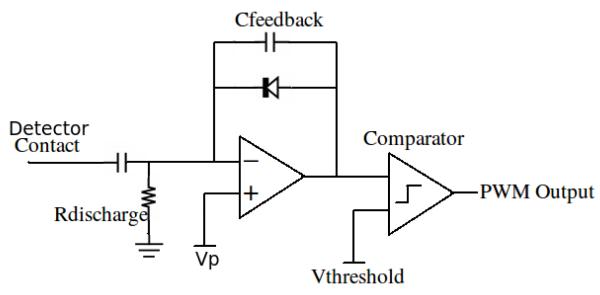
QTC PWM front ends are attractive because of their low number of components. They require only a single op-amp integrator and a comparator (see Fig. 2). However, they su er from poor signal to noise ratios and long deadtimes, because noise is integrated long after the peak of the signal pulse. Here we report on the implementation of a gated integrator PWM that uses a modified QTC with a gated, multiplexed front-end to address the problems of QTCs to reduce integrated noise, and deadtime, while allowing multiplexing (see Fig. 3).
Figure 2.
A QTC produces a digital pulse proportional to the integral of the charge coming from the detector contact with a single op-amp and comparator. The first stage integrates the input charge then discharges through Rdischarge. The comparator creates a digital pulse that starts when the integrator output falls below Vthreshold, and ends when the integrator discharges to a level above Vthreshold. This circuit was used for the “Non-gated PWM” data acquisition mode.
Figure 3.
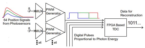
Block diagram of a multiplexed PWM scheme. Under the proposed scheme 64 position channels will be multiplexed into 8 PWM generators, then further multiplexed into just 4 readout lines to a back-end FPGA
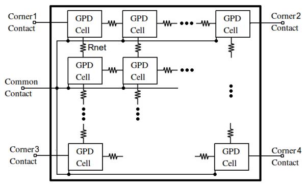
The gated integrator QTC was used to readout position sensitive solid state photo-multipliers (PS-SSPM). PS-SSPMs are CMOS based arrays of Geiger-mode photodiodes connected by a resistor network (see Fig. 4, and Table 1) (McClish et al. 2010). Each PS-SSPM has 5 outputs. Four of the outputs are position channels connected to the corners of the resistor network. Signals from these outputs are proportional to the proximity of the firing Geiger cells. These channels can be used to reconstruct the location of the sensed event. The fifth output is a common channel directly connected to each Geiger cell. The common channel signal is equal to the sum of the four position channels. In our set-up the common channel is used for timing and triggering information, while the position channels are used to position events and read their energy.
Figure 4.
A block diagram of the PS-SSPM structure. Individual Geiger-mode photodiodes are connected by a resistor mesh. The relative amplitude at the 4 corner channels is used to determine the position of the detected light. A single common channel is used for timing information. Energy information can be determined either by summing the 4 position channels or using the common contact (in this work the position channels were used).
Table 1. 5mm×5mm PS-SSPM Parameters.
| number of Geiger cells | 108×108 |
| active area per cell | 30um×30um |
| cell pitch | 44.3um×44.3um |
| fill factor | 46% |
| Rnet | 247Ohms |
| Vbias | 32V |
| Capacitance per cell | 150 fF |
| Dark Current | 10 uA/sq.mm |
The developments in this paper will be useful to researchers that are producing high resolution PET scanners and wish to reduce to complexity, size and power consumption of their readout electronics. The experiments presented were specifically aimed at designing a 3D positioning PET system using PS-SSPMs. However, other systems with high channel counts could also benefit from the methods presented.
2. Methods
The QTC consists of an op-amp integrator stage with a diode in parallel with the feedback capacitor and a discharge resistor from the op-amp’s negative input to ground (see Fig. 2). When there is no input signal to the PWM circuit the diode is on and conducts a current equal to the voltage on the pre-amp’s input divided by the discharge resistor. When there is a positive input current greater than the discharge current to the integrator the output voltage drops causing the diode to turn off. The feedback capacitor integrates the charge of the pulse then linearly discharges through the resistor until the equilibrium voltage is restored and the diode turns back on. The signal from the integrator is sent to a comparator to create the digital pulse. While a QTC is a simple and e ective method of producing PWM signals, it requires a large dead-time to discharge the feedback capacitor and is noisy due to the dark current noise, which is integrated throughout the charge up and discharge periods.
Using a gated integrator has several advantages over previous QTC implementations. 1)Gating the integrator allows the feedback capacitor to charge only during the beginning of the scintillation pulse when the signal-to-noise ratio is high (see Fig. 5 and 6). Integrating the long scintillation tail degrades noise performance and increases dead time. 2) Gating allows the discharge current to be set independent of the input signal. Without gating, all pulses with a peak current less than the discharge current cannot be seen. As a result low discharge currents must be used to preserve dynamic range. However, low discharge currents lead to noisy measurements with long dead-time. 3) Because the front-end circuit only needs to be connected when the channel is receiving a detector pulse an unlimited number channels can also be multiplexed into the same readout circuitry so long as the pulses do not overlap in time. The gated multiplexing has the advantage over other methods such as shorting detectors (Taghibakhsh et al. 2011), (Lau et al. 2010) or using charge sharing (Du et al. 2012) in that no two channels are ever coupled to each other.
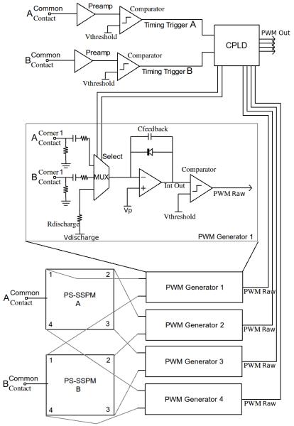
Figure 5.
Circuit diagram of a multiplexed gated integrator PWM front-end readout circuit for two PS-SSPMs (A and B). Four of the “PWM Generator” blocks were used to readout the two PS-SSPMs. This circuit was used for the “Gated PWM” data acquisition modes.
Figure 6.
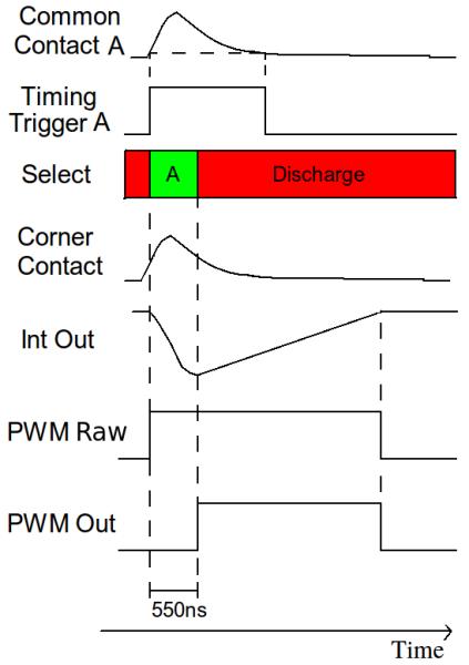
PWM circuit waveforms; each corner contact signal is integrated for 550ns before linearly discharging. The PWM output lasts from the end of integration to the end of discharge.
To control the gated integrator PWM front end the common contact was used as a trigger (see Figs. 5 and 6). If no signal is sensed a multiplexer connects the integrator input to the discharge resistor, keeping the PWM output low. Once a timing trigger occurs the CPLD logic selects the appropriate device to connect to the integrator for a set period. The integration period must belong enough to integrate charge from both fast rising signals from position channels near the event and slow rising channels far from the event (550ns in these experiments). After the integration period the multiplexer disconnects the corner contact and reconnects the integrator input to the discharge resistor which goes to a DAC supplied reference voltage that controls discharge current. The PWM pulse begins when the integration integration period ends and ends when the discharge allows the integrator signal to rise above the PWM comparator threshold. Note that at no point are any two devices connected. All the devices connected to the multiplexer can be read out without any noise coupling from one device to another.
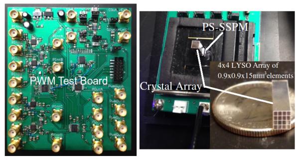
A PWM circuit was constructed using Linear Technology LTC6247 op-amps, Analog Devices ADG758 multiplexers, Maxim Max978EEE comparators, and a Xilinx XC2C32A CPLD. The board’s total power consumption was 56mW. The circuit was tested reading out two 5mm×5mm PS-SSPM produced by RMD (see Table 1)(McClish et al. 2010) coupled to a 4×4 array of 0.9mm×0.9mm×15mm LYSO crystals irradiated by Na-22 sources (see Fig. 7).
Figure 7.
(a) The test PWM circuit board. (b) A 4×4 array of 0.9mm×0.9mm×15mm LYSO crystals coupled to the 5mm×5mm area PS-SSPM
Position data was taken in five di erent modes. As a gold standard, each of the corner contact signals were digitized with a 2.5Ghz, 20GSa/sec Agilent DSO90254A oscilloscope and the pulse heights were used to produce the “Pulse Height” energy spectrum and crystal flood map. PWM data was taken without gating, “Non-gated PWM”, with gating and only a single PS-SSPM connected, “Gated PWM (Not Multiplexed)”, with gating and both PS-SSPMs connected, “Gated PWM (Multiplexed)”, and with gating andwith the PS-SSPM corner contacts shorted to the corresponding corner contact on the other PS-SSPM, “Gated PWM (Shorted)”. All experiments were performed at room temperature with no temperature regulation.
Flood maps were then created using the four position channels with the following positioning algorithm (Zhang et al. 2007):
| (1) |
| (2) |
This positioning algorithm gives well separated flood maps with reduced “pin-cushion” distortion compared to anger positioning algorithms.
Further experiments were conducted to show that the circuit maintained good timing resolution with the PWM circuit. Coincident timing resolution was measured using single 3mm×3mm×10mm LYSO crystals coupled to two PS-SSPMs with the position channels shorted to ground and with the position channel tied to the inputs of the PWM circuit. The timing data was taken by leading edge discrimination after digitizing the common channel signal with the Agilent DSO90254A oscilloscope. No position dependent timing correction algorithm was implemented.
3. Results
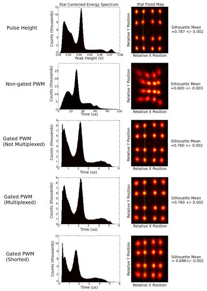
The results show that high quality energy spectra and flood maps for sub-millimeter crystals with good crystal identification can be produced using the gated integrator PWM circuit. Each of the 16 crystals can be clearly seen in each of the data acquisition modes (see Fig.8). To measure a figure of merit for crystal identification for each mode the silhouette statistic was used (Rousseeuw 1987). The silhouette for each point i is given by: where a(i) is the average squared distance from i to every other point in the crystal, and b(i) is the average squared distance from i to every other point in the nearest crystal. s(i) can be between −1 and 1, where a value of 1 corresponds to a perfect crystal flood map where all hits in a crystal are placed at exact center of crystal. The crystal flood map’s mean silhouette value is 0.787 +/− 0.002 for pulse height measurement compared to 0.600 +/− 0.003 for non-gated PWM, 0.760 +/− 0.002 for PWM with and without multiplexing, and 0.696 +/− 0.002 for PWM with shorted channels. The maximum circuit deadtime for a 511keV event was approximately 40us for non-gated PWM and 3us for gated PWM. Higher deadtimes were observed for the Na-22 source 1275keV events.
Figure 8.
The crystal corrected global energy spectra from the sum of position channels, and 511keV energy gated crystal flood maps, for each data acquisition mode reading out a 4×4 array of 0.9mm×0.9mm×15mm LYSO crystals coupled to a 5mm×5mm area PSSSPM. The non-gated PWM shows poor position resolution due to the integration of noise over its long discharge.
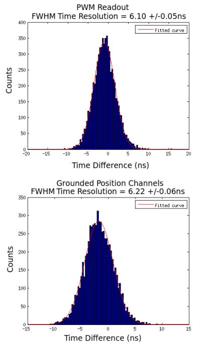
Timing resolution was not significantly a ected by the PWM readout circuit. Timing resolution taken from the common channels was 6.10 +/− 0.05ns with the position channels connected to the PWM circuit, and 6.22 +/− 0.06ns with the position channels grounded (see Fig. 9).
Figure 9.
Coincident time spectra for 3mm×3mm×10mm LYSO crystals on a 5mm×5mm PS-SSPM with time spectra taken from the common channels with the position channels connected to the PWM circuitry (Top) and with the position channels grounded (Bottom)
4. Discussion
The results show that the gated integrator technique shows a marked improvement over non-gated PWM. The dead time was reduced by a factor of 13 while the flood map silhouette mean rose by 0.160, bringing it to within 0.027 of the gold standard pulse height measurement. Gated PWM multiplexing also had no e ect on the crystal flood map quality, while multiplexing by shorting detector channels together did produce measurable degradation (Fig. 8). Shorting detector channels adds the uncorrelated noise from multiple channels into each measurement, degrading the detector’s positioning ability. It also attenuates the desired signal, because of the capacitive load of an extra PS-SSPM. Switching multiplexing does not attenuate or add noise to the signal because no two multiplexed channels are ever connected. As a result, with gated multiplexing an unlimited number of channels can be multiplexed into the same position channel readout without signal degradation as long as the channel count rate is low enough to prevent pulse pile-up. If further multiplexing is desired the dead time can be reduced by changing the discharge resistor or the time of integration. Implementing such changes to lower the deadtime should not e ect the quality of the signal as long as noise contributions of the integrator and comparator jitter are small compared to the noise of the PS-SSPM and the majority of the signal is integrated.
The timing circuitry is also una ected by multiplexing on the position channels, because the common channel does not need to be modified to implement PWM. As a result we observed very little change in timing resolution from simple leading edge discrimination with or without our PWM circuit (see Fig. 9). The timing of the PS-SSPM readout can also be improved by implementing a position dependent timing correction, or by changing the resistor mesh values in the PS-SSPM (McClish et al. 2010).
The range of energies seen is limited with our gated integrator PWM readout. Lower energies events do not have enough charge to trigger the PWM and are seen at the large background peak below 1us in Fig. 8. Higher energies are compressed when the front-end integrator rails. The Na-22 1275keV peak is misplaced as a result. The range of energies sensed by the PWM circuit can by changed by adjusting the capacitor on the integrator circuit, the dynamic range of the op-amp integrator, or the PWM comparator threshold. The cut-off at low energies means that the detector must be calibrated to find an energy resolution. For this reason no energy resolution was quoted in this work. However, the quality of the flood map shows that position channel magnitudes have been accurately measured with little added noise. As a result we expect the energy resolution of our PWM electronics to be comparable to traditional readout for PS-SSPMs.
While this circuit is designed for use with PS-SSPMs the concept could be used for non-position sensitive devices. Instead of having circuitry on every SiPM for energy measurements, each device could have its own timing trigger, and share the energy circuitry in a similar fashion to this work. Gated strategies could also be used to decrease the complexity of time-over-threshold systems as well as PWM systems.
5. Conclusions
We have shown a compact, multiplexed PWM circuit based on a gated integrator that shows improvements in position resolution and dead time over non-gated QTCs and has successfully identified sub-millimeter width crystals coupled to a PS-SSPM. Multiplexing with our gated integrator front-end shows no crystal flood histogram degradation in contrast to multiplexing two PS-SSPMs by shorting corresponding channels together. The latter su ers from signal attenuation due to the device capacitance and added uncorrelated noise from the two devices. In the future we plan to try the gated-integrator technique on larger area PS-SSPMs with smaller crystals, and multiplex the readouts of many more PS-SSPMs. This work will facilitate the creation of a 0.5mm resolution PET system with a compact PWM readout, and could lead to simplification of readout for existing detectors.
Acknowledgments
This work was supported in part by NIH research grant R01 EB011552 and NIH training grant T32 EB009653.
References
- Fujiwara T, Takahashi H, Shimazoe K, Shi B. Multi-Level Time-Over-Threshold Method for Energy Resolving Multi-Channel Systems. IEEE TNS. 2010:2545–8. [Google Scholar]
- Du J, et al. A Novel Capacitive Charge-Division Readout for Position-Sensitive Solid-State Photomultiplier Array. IEEE NSS/MIC. 2012 doi: 10.1109/TNS.2013.2275012. [DOI] [PMC free article] [PubMed] [Google Scholar]
- Hong K, Kim E, Yeom JY, Levin1 CS. FPGA-Based Time-to-Digital Converter for Time-of-Flight PET detector. IEEE NSS/MIC. 2012:M09–60. [Google Scholar]
- Lau F, Vandenbroucke A, Reynolds P, Olcott P, Horowitz M, Levin C. Analog Signal Multiplexing for PSAPD-based PET Detectors: Simulation and Experiemntal Validation. Phys. Med. Biol. 2010;55:7149–71774. doi: 10.1088/0031-9155/55/23/001. [DOI] [PMC free article] [PubMed] [Google Scholar]
- Levin C. Promising New Photon Detection Concepts for High-Resolution Clinical and Preclinical PET. J Nucl Med. 2012;53:167170. doi: 10.2967/jnumed.110.084343. [DOI] [PMC free article] [PubMed] [Google Scholar]
- McClish M, Dokhale P, Christian J, Stapels C, Johnson E, Robertson R, Shah K. Performance Measurements of CMOS Position Sensitive Solid-State Photomultipliers. IEEE TNS. 2010:2280–6. [Google Scholar]
- Mintzer R, Siegel S. Design and Performance of a New Pixelated- LSO/PSPMT Gamma-Ray Detector for High Resolution PET Imaging. IEEE NSS/MIC. 2007:3418–22. [Google Scholar]
- Olcott P, Levin CS. Pulse Width Modulation: A Novel Readout Scheme for High Energy Photon Detection. IEEE NSS/MIC. 2008:4530–5. [Google Scholar]
- Rousseeuw P. Silhouettes: a graphical aid to the interpretation and validation of cluster analysis. J Comp and Applied Mathematics. 1987;20:53–65. [Google Scholar]
- Schmall J, Du J, Yang Y, Dokhale P, McClish M, Christian J, Shah K, Cherry S. Comparison of Large-area Position-Sensitive Solid-State Photomultipliers for Small Animal PET. Phys. Med. Biol. 2012;57:8119–8134. doi: 10.1088/0031-9155/57/24/8119. [DOI] [PubMed] [Google Scholar]
- Shimazoe K, Nguyen H, Orita T, Wang Y, Shi B, Suzuki T, Takahashi H. Application of Dynamic Time-over-Threshold Method to Pixellated CdTe Detector. IEE NSS/MIC. 2010:3888–90. [Google Scholar]
- Streun M, Larue H, Parl C, Ziemons K. A Compact PET Detector Readout Using Charge-to-Time Conversion. IEE NSS/MIC. 2009:1868–70. [Google Scholar]
- Taghibakhsh F, Levin CS. Novel Techniques of Multiplexing Position Sensitive Solid State Photomultipliers for High Resolution. PET IEEE NSS/MIC. 2011 [Google Scholar]
- Vandenbroucke A, Mclaughlin TJ, Levin CS. Influence of Temperature and Bias Voltage on the Performance of a High Resolution PET Detector Built with Position Sensitive Avalanche Photodiodes. Jinst. 2012;7:P08001. [Google Scholar]
- Zhang J, Olcott P, Levin C. A New Positioning Algoritm for Position-Sensitive Avalanche Photodiodes. IEEE TNS. 2007;54(3):433–7. doi: 10.1109/TNS.2007.894129. [DOI] [PMC free article] [PubMed] [Google Scholar]


