Abstract
Here we introduce a new paradigm of far-field optical lithography, optical force stamping lithography. The approach employs optical forces exerted by a spatially modulated light field on colloidal nanoparticles to rapidly stamp large arbitrary patterns comprised of single nanoparticles onto a substrate with a single-nanoparticle positioning accuracy well beyond the diffraction limit. Because the process is all-optical, the stamping pattern can be changed almost instantly and there is no constraint on the type of nanoparticle or substrates used.
Keywords: optical lithography, optical forces, spatial light modulator, colloidal nanoparticles
Optical lithography techniques are widely used to fabricate nanoscale devices for optoelectronics, biological and medical applications1,2,3. The lateral feature size achievable by conventional far-field optical lithography is diffraction-limited4. A number of far-field approaches have been proposed to overcome the diffraction limit5,6,7,8, but these are not suitable for arbitrary pattern formation. Scanning near-field optical microscopy techniques can also go beyond the diffraction limit9,10,11,12, but due to their serial essence the scanning methods suffer from low throughput and limited patterning areas.
An elegant way of manipulating small particles is to employ the optical forces exerted by light on micro- and nanoobjects upon interaction with them. These forces can be used to optically trap individual particles by a tightly focused laser beam13, move them to target positions and, finally, fix them onto a substrate by various mechanisms14,15,16. Although this approach offers wide flexibility in assembling arbitrary patterns composed of particles, it is of limited use for mass production due to its extremely low throughput and inherent complexity of manipulation of several simultaneously trapped particles. In Optical Force Stamping Lithography (OFSL) the optical forces are not used to optically trap nanoparticles. Instead by using the repulsive force exerted by a laser beam resonant to nanoparticles’ extinction maxima17,18, the nanoparticles are accelerated along the directions of the light energy flux and fixed at desired positions on a substrate19,20.
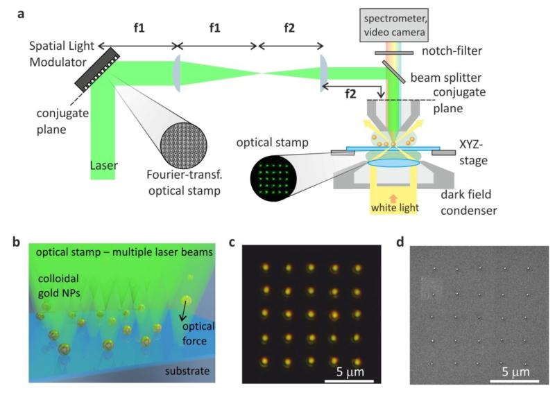
OFSL is an all-optical, far-field and maskless technique offering high flexibility for surface processing over large areas using tailored colloidal micro- and nanoparticles with desired optical, electric and magnetic properties. The method merges advantages of optical far-field lithography and colloidal chemistry by applying a two step fabrication of nanoscale devices. First, individual components of the future device with required properties and functionalities are prepared using well established colloidal synthesis protocols21,22. These components are then arranged on a substrate by light which enables an easy parallelization of this process. The concept of OFSL can be defined as follows: a spatial light modulator (SLM) is used to split a laser beam into several beams, creating an optical pattern, which is focused onto a substrate through a colloidal solution of the nanoparticles which are to be deposited (Fig. 1a). The nanoparticles, tailored to be electrostatically repelled by the substrate, are captured from the solution by the laser beam, guided towards the substrate and then attached to it at the desired position. The laser helps the nanoparticles overcome the electrostatic repulsion, upon which they bind via van der Waals attraction to the substrate19 forming a pattern predefined by the optical stamp (Fig. 1b). An example of this process is shown in Fig 1c,d, where OFSL was employed to stamp a square 5×5 pattern of equally spaced 80 nm gold nanoparticles onto a bare glass substrate. This pattern was stamped rapidly, in just ten seconds and the deposited nanoparticles show a spatial deviation from the desired positions of smaller than 45 nm, less than λ/10 of the laser wavelength of 532 nm.
Figure 1. Deposition of gold nanoparticles by optical force stamping lithography.
a, Sketch of the optical force stamping setup. 4f-imaging is used to transfer the Fourier image of the optical stamp from a spatial light modulator to the back focal plane of a microscope objective. An optical microscope with dark-field illumination and a water immersion objective is used for imaging of the stamping process. b, Schematic of the optical force stamping process: colloidal nanoparticles are caught from a suspension, pushed toward deposition positions and ultimately bound to the substrate through Van-der Waals forces c, A dark-field image of a 5×5 pattern of 80 nm gold nanoparticles stamped on a glass substrate. Each bright spot on this image corresponds to a single gold nanoparticle. d, A scanning electron microscopy image of a 5×5 pattern of 80 nm gold nanoparticles on a glass substrate.
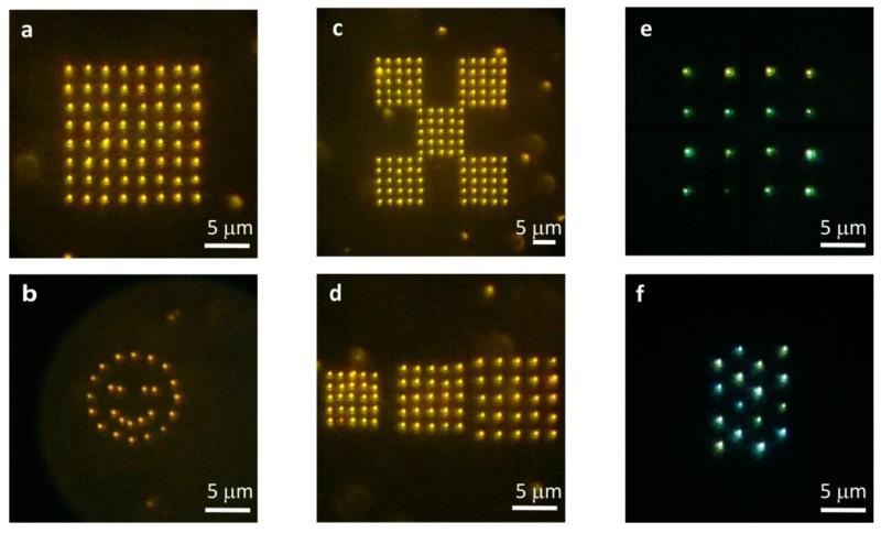
OFSL offers a high deposition throughput for two reasons. Firstly, there is no fundamental constraint on the dimensions of or the number of spots encoded within the optical stamp. Secondly, the stamping process for each nanoparticle is independent of the other nanoparticles. Therefore, the time needed to stamp a pattern is almost independent on its size. An 8×8 pattern composed of 64 nanoparticles took only 11 seconds to be completed (Fig. 2a), almost the same time required to print the aforementioned 5×5 pattern. A clear advantage in comparison with other lithographic techniques is the possibility in OFSL to form irregular, arbitrary patterns composed of nanoparticles without a need to design a mask (Fig. 2b). It is worth noting that the stamping speed is dependent on the concentration of nanoparticles in the solution and thus can be easily tuned in a wide range.
Figure 2. Versatility of optical force stamping lithography.
Dark-field images of patterns stamped on a glass substrate: a, A square 8×8 and b, an arbitrary “smiley” pattern both composed of single 80 nm gold nanoparticles. c, Five square 5×5 patterns stamped sequentially in a chess board like manner by shifting the Fourier image displayed at the SLM. d, Three sequentially stamped square 5×5 patterns with different pitch size. Both the pitch size and the position of the pattern are controlled by the SLM. e, A square and f, a hexagonal pattern comprised of 80 nm silver nanoparticles. A cw-laser operating at 532 nm is used to stamp these patterns. A real-time video showing the stamping process of an 8×8 pattern is available in the Supporting information.
As with a common stamp, the same pattern can be repeatedly stamped at different locations on a substrate by slightly modifying the image displayed on the SLM thereby forming more complex patterns (Fig. 2c). A feature unique to OFSL is the ability to swiftly change the shape of the optical stamp and form different shaped patterns on the substrate (Fig. 2d). Thus, macroscopically large area stamping can be achieved by controlling the position of the optical pattern on the substrate with a piezo stage and repeating the stamping process
Another essential requirement of a technique used to fabricate devices is the ability to deposit nanoparticles with different properties and functionalities. As mentioned before, OFSL offers this possibility as well. To demonstrate this 80 nm silver nanoparticles were used to stamp 4×4 arrays with different lattice symmetries (Fig. 2e, f). To stamp the silver nanoparticles the laser power per stamping point was increased to compensate for the smaller extinction cross-section at 532 nm of silver compared to gold nanoparticles. Thus it is possible to sequentially stamp different types of nanoobjects onto one substrate by exchanging the solution after each stamping cycle. However, it is even possible to print different nanoparticles from the same solution. This can be done, because the magnitude of the optical force exerted on a nanoparticle reaches a maximum when the laser wavelength is tuned to the nanoparticle’s extinction spectra.18 Thus one may employ several lasers with wavelengths tuned to the extinction spectrum maxima of each type of nanoparticle.
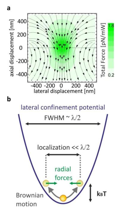
Despite OFSL being a far-field method it is capable of producing structures with an accuracy well beyond the diffraction limit. Because the feature size can be fine-tuned with nanometric precision through colloidal chemistry, the only inaccuracy results from the positioning of the nanoparticles. As aforementioned, the achieved accuracy is better than 45nm. The reason for this remarkable accuracy is two-fold and lies in the nature of the optical force stamping method. The optical force exerted by a focused laser beam on a metallic particle can be split into two components: (i) axial – along the beam propagation direction and (ii) radial – towards the beam axis. The axial component, which affixes the nanoparticles to the substrate surface, has a Gaussian-shaped intensity profile. Thus, the size of the area in the proximity of beam axis inside which the optical force is strong enough to stamp the nanoparticles is controlled by regulating the intensity of the laser beam. Even more important, the radial force is attractive. It guides the nanoparticles toward the beam axis and holds them near the center of the beam. Effectively the radial component of the optical force confines the nanoparticles in a two-dimensional potential well (Fig. 3b). The full width at half maximum (FWHM) of this well is diffraction limited, but its depth is directly proportional to the total beam power. The nanoparticles are restricted by the radial optical forces to move laterally due to the Brownian motion only at the very bottom of the well, realizing the sub-diffraction limited confinement of the nanoparticles. The confinement can be tuned by adjusting the beam power to enable virtually any required positioning accuracy. Analogous to localization microscopy techniques measuring absolute positions of dye molecules with precision well below the diffraction limit, the accuracy can theoretically be reduced down to a few nanometers23. The deposition inaccuracy reported here is mostly due to astigmatism of the SLM and aberrations of the imaging optics. Both of these issues can be compensated in future to improve the accuracy down to a few nanometers24.
Figure 3. Optical force stamping lithography enables accuracy beyond the diffraction limit.
a, Spatial distribution of the optical forces exerted by a tightly focused Gaussian beam on an 80 nm gold nanoparticle. The numerical aperture of the focusing lens is 1.0. The color encodes the magnitude of the force and the arrows the direction. b, Schematic of a gold nanoparticle trapped laterally by the radial optical forces enabling the superior accuracy of optical force stamping lithography.
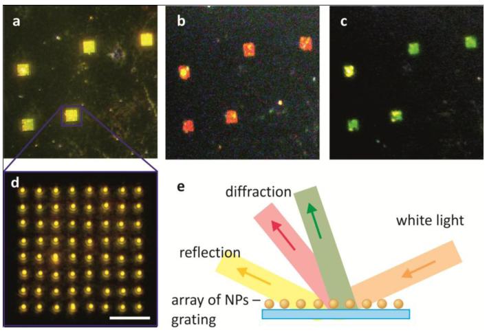
To test the capability of OFSL for microdevice fabrication and being inspired by the strong attention given recently by the scientific community to arrays of metallic nanoparticles3,25,26, we have stamped several diffraction gratings composed of single gold nanoparticles on a glass substrate (Fig. 4). Under dark-field illumination and observed through a low-magnification/low-NA objective lens these arrays have the same yellowish color (Fig. 4a) as the individual gold nanoparticles seen in a high magnification/high-NA objective lens (Fig. 4d). Under grazing incidence of the illumination beam (Fig. 4e) the arrays appear in different colors depending on the angle of incidence (Fig 4b,c). Consequently, despite a size of only 14×14 μm and a fabrication time of ten seconds each, the arrays fully function as diffraction gratings.
Figure 4. Diffraction gratings stamped by optical force stamping lithography.
a, Dark-field image of five stamped diffraction gratings composed of 80 nm gold nanoparticles. b, c, Scattering images of the gratings taken with a low NA objective at slightly different angles of incidence. A halogen lamp was used to illuminate the gratings. d, Dark-field image of a diffraction grating taken at higher magnification. e, Schematic of light diffraction by an array of stamped nanoparticles. Scale bar is 5μm.
In conclusion, we have introduced a new type of far-field optical lithography for producing patterns with nanometric accuracy. The new approach is based on deposition of colloidal nanoparticles from a solution by the optical forces exerted by a spatially modulated optical field, called an optical stamp. The method is very versatile, enabling low-cost and high-throughput stamping of large and arbitrary patterns composed of nanoparticles with different functional properties on substrates. As a proof-of-concept several functional micro diffraction gratings have been stamped with an accuracy of only a few tens of nanometers and in less than a minute using optical force stamping lithography. Further developments could extend this technique into the third dimension enabling more complex multi-level architectures. Due to the high patterning accuracy and versatility of the OFSL, it has potential to compete with e-beam lithographic and scanning-probe techniques for producing nanostructures. Providing the nanometric accuracy, this technique is essentially a single step method operating at ambient conditions and not requiring ultra-high vacuum or deep ultra-violet radiation. Additionally, OFSL is operational in aqueous media providing ease of integration into biological, medical and chemical applications.
Methods
Experimental setup
The optical force stamping lithography setup (Fig. 1a) is composed of a spatial light modulator (HoloEye LC-R 2500), a water immersion objective (Zeiss W Achroplan 100x/1.0 W/0), an inverted microscope (Zeiss Axiovert) equipped with a dark-field illumination condenser and a 532 nm cw-laser (Coherent Verdi-V10). A dichroic beam splitter (Semrock Di01-R532-25×36) is used to filter out scattering from the laser. Images are recorded with a digital camera (Panasonic Lumix DMC-FZ50). The optical stamp is formed by the spatial light modulator LC-R 2500 which is based on a reflective LCOS (Liquid-Crystal-On-Silicon) micro-display. It is capable of spatially modulating the amplitude and/or phase of the reflected light by displaying computer-generated holograms. The SLM forms a pattern of discrete laser beams on a substrate by means of 4f imaging of the SLM surface plane to the back focal plane of a microscope objective lens (Fig. 1a). In this configuration an image of the desired pattern is Fourier-transformed, displayed on the SLM and transferred to the back focal plane of the imaging objective. The objective, in turn, performs a reverse Fourier transform to its front focal plane and forms the optical stamp on the substrate surface. The objective lens is immersed directly in a solution containing the nanoparticles which are to be stamped and is focused onto the substrate. Laser power in the range of 2.5-3.5 mW per stamp point behind the objective was used to stamp nanoparticles on a substrate. To shift the stamp in the image plane a blazed holographic grating is added to the displayed Fourier pattern
Samples
37 μl of a solution (3.1×10⁵ nps/ml) of gold nanoparticles (82 nm in diameter, Nanopartz) or silver nanoparticles (80 nm in diameter, BBInternational) were enclosed between the microscope objective and a silica cover slip. Standard 0.17 mm cover slips were washed in acetone, isopropanol and water, dried using a nitrogen gun and treated in a plasma etcher.
Characterization of diffraction gratings was performed using a low-NA, low magnification objective (NA= 0.075, M=2.5x) in an upright dark field microscope and illuminating the gratings from the side at low angles with respect to the cover slip plane. By varying the angle of illumination the microscope objective collects different wavelengths of the scattered light in the first order.
Supplementary Material
Acknowledgements
We are thankful to our colleagues A. Deak for SEM imaging, and to E. Da Como, F. Jäckel and T. Lohmüller for reading the manuscript and their helpful comments. Financial support by the DFG through the Nanosystems Initiative Munich (NIM), by the ERC through the Advanced Investigator Grant HYMEM and by the EU through the research training network ICARUS is gratefully acknowledged.
References
- 1.Ito T, Okazaki S. Pushing the limits of lithography. Nature. 2000;406:1027–1031. doi: 10.1038/35023233. [DOI] [PubMed] [Google Scholar]
- 2.Saavedra HM, et al. Hybrid strategies in nanolithography. Rep. Prog. Phys. 2010;73:036501. [Google Scholar]
- 3.Leggett GJ. Direct Writing of Metal Nanostructures: Lithographic Tools for Nanoplasmonics Research. ACS Nano. 2011;5:1575–1579. doi: 10.1021/nn2006442. [DOI] [PubMed] [Google Scholar]
- 4.Abbe E. Beiträge zur Theorie des Mikroskops und der mikroskopischen Wahrnehmung. Archiv f. mikrosk. Anatomie. 1873;9:413–418. [Google Scholar]
- 5.Scott TF, Kowalski BA, Sullivan AC, Bowman CN, McLeod RR. Two-Color Single-Photon Photoinitiation and Photoinhibition for Subdiffraction Photolithography. Science. 2009;324:913–917. doi: 10.1126/science.1167610. [DOI] [PubMed] [Google Scholar]
- 6.Li L, Gattass RR, Gershgoren E, Hwang H, Fourkas JT. Achieving λ/20 Resolution by One-Color Initiation and Deactivation of Polymerization. Science. 2009;324:910–913. doi: 10.1126/science.1168996. [DOI] [PubMed] [Google Scholar]
- 7.Perry JW. Two Beams Squeeze Feature Sizes in Optical Lithography. Science. 2009;324:892–893. doi: 10.1126/science.1174224. [DOI] [PubMed] [Google Scholar]
- 8.Zhang X, et al. Holographic Control of Motive Shape in Plasmonic Nanogap Arrays. Nano Lett. doi: 10.1021/nl200994k. ASAP Article (2011).doi:10.1021/nl200994k. [DOI] [PubMed] [Google Scholar]
- 9.Naber A, Kock H, Fuchs H. High-Resolution Lithography with Near-Field Optical Microscopy. Scanning. 2006;18:567–571. [Google Scholar]
- 10.Leggett GJ. Scanning near-field photolithography surface photochemistry with nanoscale spatial resolution. Chem. Soc. Rev. 2006;35:1150. doi: 10.1039/b606706a. [DOI] [PubMed] [Google Scholar]
- 11.Kingsley JW, Ray SK, Adawi AM, Leggett GJ, Lidzey DG. Optical nanolithography using a scanning near-field probe with an integrated light source. Appl. Phys. Lett. 2008;93:213103. [Google Scholar]
- 12.Huo F, et al. Beam pen lithography. Nature Nanotech. 2010;5:637–640. doi: 10.1038/nnano.2010.161. [DOI] [PubMed] [Google Scholar]
- 13.Ashkin A, Dziedzic JM, Bjorkholm JE, Chu S. Observation of a single-beam gradient force optical trap for dielectric particles. Opt. Lett. 1986;11:288–290. doi: 10.1364/ol.11.000288. [DOI] [PubMed] [Google Scholar]
- 14.Svedberg F, Li Z, Xu H, Käll M. Creating Hot Nanoparticle Pairs for Surface-Enhanced Raman Spectroscopy through Optical Manipulation. Nano Lett. 2006;6:2639–2641. doi: 10.1021/nl062101m. [DOI] [PubMed] [Google Scholar]
- 15.Ito S, Yoshikawa H, Masuhara H. Laser manipulation and fixation of single gold nanoparticles in solution at room temperature. Appl. Phys. Lett. 2002;80:482. [Google Scholar]
- 16.Guffey MJ, Scherer NF. All-Optical Patterning of Au Nanoparticles on Surfaces Using Optical Traps. Nano Lett. 2010;10:4302–4308. doi: 10.1021/nl904167t. [DOI] [PubMed] [Google Scholar]
- 17.Agayan RR, Gittes F, Kopelman R, Schmidt CF. Optical trapping near resonance absorption. Appl. Opt. 2002;41:2318. doi: 10.1364/ao.41.002318. [DOI] [PubMed] [Google Scholar]
- 18.Arias-González JR, Nieto-Vesperinas M. Optical forces on small particles: attractive and repulsive nature and plasmon-resonance conditions. J. Opt. Soc. Am. A. 2003;20:1201. doi: 10.1364/josaa.20.001201. [DOI] [PubMed] [Google Scholar]
- 19.Urban AS, Lutich AA, Stefani FD, Feldmann J. Laser Printing Single Gold Nanoparticles. Nano Lett. 2010;10:4794–4798. doi: 10.1021/nl1030425. [DOI] [PubMed] [Google Scholar]
- 20.Urban AS, Pfeiffer T, Fedoruk M, Lutich AA, Feldmann J. Single-Step Injection of Gold Nanoparticles through Phospholipid Membranes. ACS Nano. 2011;5:3585–3590. doi: 10.1021/nn201132a. [DOI] [PMC free article] [PubMed] [Google Scholar]
- 21.Weller H. Synthesis and Self-Assembly of Colloidal Nanoparticles. Philosophical Transactions: Mathematical, Physical and Engineering Sciences. 2003;361:229–240. doi: 10.1098/rsta.2002.1136. [DOI] [PubMed] [Google Scholar]
- 22.Caruso F. Colloids and colloid assemblies: synthesis, modification, organization and utilization of colloid particles. Wiley-VCH; 2004. [Google Scholar]
- 23.Yildiz A. Myosin V Walks Hand-Over-Hand: Single Fluorophore Imaging with 1.5-nm Localization. Science. 2003;300:2061–2065. doi: 10.1126/science.1084398. [DOI] [PubMed] [Google Scholar]
- 24.Jesacher A, et al. Wavefront correction of spatial light modulators using an optical vortex image. Opt. Express. 2007;15:5801. doi: 10.1364/oe.15.005801. [DOI] [PubMed] [Google Scholar]
- 25.Lamprecht B, et al. Metal Nanoparticle Gratings: Influence of Dipolar Particle Interaction on the Plasmon Resonance. Phys. Rev. Lett. 2000;84:4721–4724. doi: 10.1103/PhysRevLett.84.4721. [DOI] [PubMed] [Google Scholar]
- 26.Zhou W, Odom TW. Tunable subradiant lattice plasmons by out-of-plane dipolar interactions. Nature Nanotech. 2011 doi: 10.1038/nnano.2011.72. doi:10.1038/nnano.2011.72. [DOI] [PubMed] [Google Scholar]
Associated Data
This section collects any data citations, data availability statements, or supplementary materials included in this article.


