Abstract
Modern field programmable gate arrays (FPGAs) are capable of performing complex discrete signal processing algorithms with clock rates well above 100 MHz. This, combined with FPGA’s low expense, ease of use, and selected dedicated hardware make them an ideal technology for a data acquisition system for a positron emission tomography (PET) scanner. The University of Washington is producing a high-resolution, small-animal PET scanner that utilizes FPGAs as the core of the front-end electronics. For this scanner, functions that are typically performed in dedicated circuits, or offline, are being migrated to the FPGA. This will not only simplify the electronics, but the features of modern FPGAs can be utilized to add significant signal processing power to produce higher quality images. In this paper we report on an all-digital pulse pile-up correction algorithm that has been developed for the FPGA. The pile-up mitigation algorithm will allow the scanner to run at higher count rates without incurring large data losses due to the overlapping of scintillation signals. This correction technique utilizes a reference pulse to extract timing and energy information for most pile-up events. Using pulses acquired from a Zecotech Photonics MAPD-N with an LFS-3 scintillator, we show that good timing and energy information can be achieved in the presence of pile-up utilizing a moderate amount of FPGA resources.
Keywords: Digital signal processing, field programmable gate arrays, imaging, integrated circuits, nuclear medicine, parameter estimation, positron emission tomography, signal analysis, time of arrival estimation
I. Introduction
WE are developing a second-generation data acquisition system to support several positron emission tomography (PET) designs being developed at the University of Washington [1]. It is based on our experience with the original MiCES electronics concepts [2]. Along with the development of the hardware, we are also developing algorithms for the field programmable gate array (FPGA) that will make up the core of the front-end electronics. In previous work, we have developed algorithms for statistical event location [3], digital timing [4], and automated pulse parameter discovery [5].
The main goal of this and previous work is to develop an all-digital FPGA-based signal processing suite for a small animal PET scanner. The addition of a pulse pile-up correction routine will allow us to investigate experiments with higher count rates. This will be especially important for experiments that use a continuous scintillator crystal [6] or readout electronics with row-column summing. We are currently experimenting with scanner architectures that have both of these features. In [7] we show how a common anode timing channel for an MAPD-N array can be built. While this will lower the number of timing channels in the system, a common anode will increase the likelihood of pile-up. The common anode is essentially a summation of all of the channels of a detector. So, if two interactions occur anywhere within a detector in the timeframe of a single pulse, pile-up will occur on the common anode.
II. Previous Work
In order to extract timing and energy information from a pile-up event, the multiple pulses need to be separated. There have been previous analog and digital circuits implemented to recover from pulse pile-up. The first analog method uses a dynamic integration technique to retrieve the energy information from a pile-up event [8]. Dynamic integration uses an analog circuit to integrate a pulse until it detects a pile-up event, at which point it starts a new integration. To get the total energy value, the remaining tail of the first pulse is interpolated. The interpolated tail of the first pulse is subtracted from the second integration to resolve the energy of the second pulse. The high yield pile-up event recovery (HYPER) method corrects for multiple pulse pile-up events by computing a weighted sum of an overlapping pulse and subtracting the weighted sum of the previous pulses, decreased by a time-decay term [9]. This method requires analog components and an integrator that clears when a pile-up event occurs. This method has recently been converted into a digital implementation in an FPGA [10]. In order to achieve good energy resolution in a digital circuit, HYPER needs ADC rates of at least 200 Msps, as well as an analog trigger to signal the beginning of any pulse. Of course, pulse pile-up is not a problem just for PET detectors, high-energy physics detectors can benefit from pile-up mitigations [11], [12].
Finally, after our technique in this paper was developed and the detailed implementation was studied, it was determined that a patent [13] exists that proposes a similar idea of pile-up correction. This patent is targeted to gamma cameras, so the ability to timestamp pulses was not proposed as we do in this work. The main concern of the patent was to obtain energy information from pile-up events. So, instead of actually separating the pulses (as this work does) only the energy contribution of individual pulses wass calculated. As the following sections will show, in order to timestamp pulses involved in pile-up the pulses need to be separated. Additionally, the patent covers the general idea but gives no implementation details.
III. General Algorithm
The work presented here will build upon our all-digital timing algorithm [4]. In this previous work, we utilize a high-resolution reference pulse that has the same shape as the scintillation pulses arriving from the ADC to timestamp each pulse. The reference pulse is used as a look-up table to estimate the start time of the pulse based on the voltage of the sample(s) on the leading edge of the data pulses from the ADC.
To eliminate time walk, the amplitude of the data pulses from the ADC are normalized to the reference pulse. This is accomplished by normalizing the area under the two pulses. Using the area to normalize the amplitude works well at low sampling rates when the peak may not be sampled and it also reduces the affects of noise. The downside, as we will illustrate, is that it requires the entire pulse to be summed without pileup.
The next step is to time stamp the pulse. We accomplish this by converting the reference pulse into a look-up table. This table is indexed by the voltage of the reference pulse, and the data stored at each voltage is how far from the start of the pulse in time does it take for the reference pulse to get to that voltage. When this table is used in the timing algorithm, one or more on the samples on the leading edge of the data pulse are used to address the look-up table and the output is combined with a coarse grain timing to get the time stamp.
In [5], we show how this reference pulse can be built in the FPGA out of the same pulses on which it will be used. The time-stamp comes from a lookup table that stores the time elapsed from the start of the reference pulse based on the voltage of a sample.
Based on this prior work, we aim to develop a pulse pile-up correction algorithm on an all-digital platform that recovers the start time and energy of each individual pulse involved in pile-up. Our proposed method uses a combination of pulse shape discrimination and partial dynamic integration to detect and remove peak pile-up (pile-up where two pulses start so close together that they cannot be separated) and to correct for tail pile-up (pile-up where the second pulse starts in the tail of the first pulse).
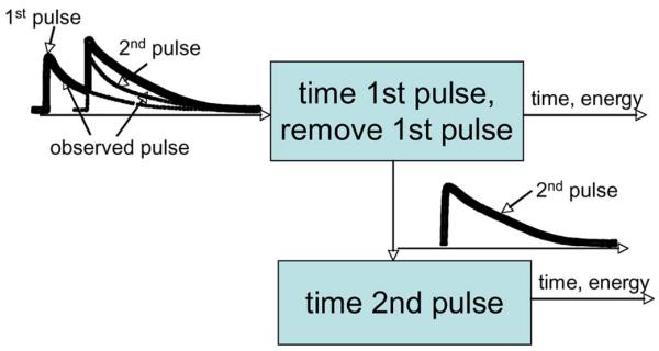
Fig. 1 shows the general structure of the algorithm for pile-up correction. As a pulse is detected, the time stamp and pulse energy are calculated. After this, the processed pulse is removed from the data stream, which is sent to a second processing engine. By removing the first pulse, any pile-up event present will be separated so that the second engine can process it for start time and energy. If no pile-up is present, then the second engine will receive a flat signal. To remove the first pulse from the stream, the reference pulse is used to interpolate the tail of the first pulse that is hidden under any pile-up event.
Fig. 1.
Block diagram of the overall pulse pile-up correction algorithm.
The number of stages present in the algorithm is dependent on the amount of pile-up events expected. For example, if the probability of having a pile-up event that contains four pulses is less than 1%, then it probably is not necessary to have more than three processing engines. The probability cutoff is a designer choice and is easy to change, as the stages are identical.
To determine the start time of the pulse, the timing algorithm [4] has to be modified, as the whole pulse can no longer be used to normalize its amplitude. Instead of using the whole pulse, only the area under the first portion of the pulse is used. The point that the summing is stopped will be designated as the transition from peak to tail pile-up. This means that we will try to mitigate any pile-up after this cutoff, and remove any pile-up before. The lookup table for area to amplitude normalization must be modified to reflect this change. In other words, when comparing the area of the data pulse to the reference pulse, the same number of samples is used in both summations. The time lookup does not have to be modified.
To eliminate pulses involved in peak pile-up, the energy is checked to determine whether it is below the expected energy maximum that was determined in the reference pulse discovery routine. The idea is that if a second pulse starts before the cutoff, then it will add energy to the summation. If it is determined that peak pile-up has occurred, both pulses are discarded and the system is dead until the incoming data stream returns to baseline.
Once the first pulse is time stamped, it can be removed from the data stream. Because only tail pile-up after the area summation cutoff will be corrected, only the samples after the cutoff need to be removed from the stream and the downstream engine only needs to process data after the cutoff for the above engine. This also means that the system can run in real-time, as no past data needs to be sent to the downstream engines. In this algorithm, it is assumed that pile-up will occur, so the reference pulse is always used to remove the tail of the first pulse from the stream. The timestamp is used to determine what samples from the reference pulse to use. The reference pulse is defined at a much finer resolution (every 60 ps in this work) than the sampling rate of the ADC (16 ns-1 ns). The data that is sent to the next processing engine is calculated using (1):
| (1) |
Here, vinput is the data stream from the ADC, vref is the reference pulse voltage, n is the number of ADC samples summed on the leading edge of the pulse for the amplitude normalization, ((ts)/(tADC)) is the ratio of reference pulse resolution to ADC resolution,Δt is the result of the time stamp lookup table (i.e., how far the first sample was from the start of the pulse) and ((Ap)/(Ar)) is the normalization factor to normalize the reference pulse amplitude to the first incoming pulse amplitude.
Partial dynamic integration is used to determine the energy of the pulse. Two summations are generated for each pulse, one to the cutoff point and one for the full pulse. If the downstream engine indicates that pile-up did occur, then the cutoff summation energy is calculated by using the partial summation, with the remaining pulse energy calculated from the reference pulse as indicated above. If no pulse is detected in the downstream engine, then the whole pulse summation is used. This scheme requires a termination processing engine that simply indicates whether it has detected a pulse, but does not process it. This engine would be in addition to the max number of expected consecutive pile-ups.
IV. Tests AND Methods
A. Determining Peak Pile-Up Cutoff
The first step in developing this algorithm is to determine where to set the cutoff between peak and tail pile-up. We started by investigating how much of the leading edge of the pulse is needed to accurately calculate the area to amplitude normalization and interpret the tail of the pulse. In our original timing routine, all of the samples of the pulse are summed. The ratio of this sum and the equivalent sum of the reference pulse is then used to normalize the amplitude of the data pulse to the reference pulse to reduce time walk. In the event of tail pile-up, all of the samples are not available, so the question is how many samples free from pile-up are needed to perform this normalization step. The accuracy may degrade as less of the pulse is used, but using less of the pulse reduces the dead time, so the tradeoff between dead time and energy/timing resolution has to be balanced. To perform this, a simulation was performed in Matlab using 1000 unfiltered pulses from different pixels on a Zecotech MAPD-N with a LFS-3 scintillator. The MAPD-N has 15 000 pixels/mm2, a breakdown voltage of 89 V and a dark count rate of ≤ 100 LFS-3 has a density of 7.35 g/cm3, a maximum emission at 435–438 nm and a light yield of 80%–85% on the NaI scale. The raw pulses from this combination have a 310 ps rise time and a 34.5 ns decay time.
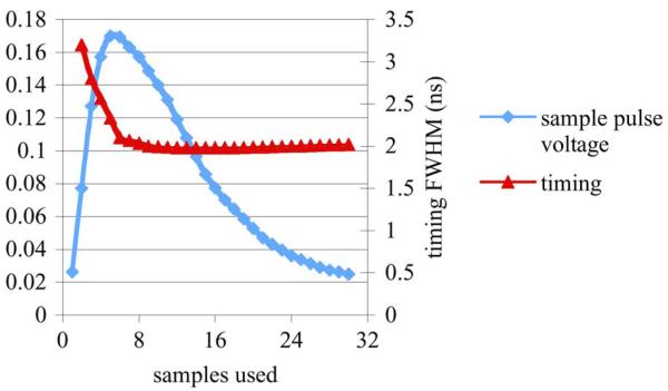
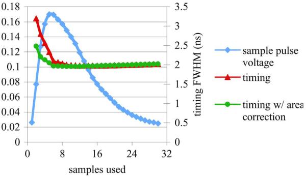
To determine the effect on timing resolution, two streams were created with the pulses in each stream in coincidence. The original timing algorithm [4] was run, except only a portion of the pulse was summed and that area was used to normalized the amplitude. The amount that was summed was swept from 100% to about 5%. Fig. 2 shows the results of this study. A sample pulse is included to provide a reference of what part of the pulse is being summed. The x-axis indicates how much of the pulse (in samples) is being summed up for amplitude normalization. For this sampling rate (65 MHz) and pulse length, 32 samples constitutes summing up 100% of the pulse, while 2 samples corresponds to about 5% of the pulse (it does not make sense to use just one sample). Notice that the timing resolution remains fairly flat until the cutoff point approaches the peak. If the summing is stopped before the peak, the timing resolution is substantially degraded, as would be expected.
Fig. 2.
Graph of timing resolution for different amount of pulse used for amplitude normalization for a 65 MHz sampled pulse.
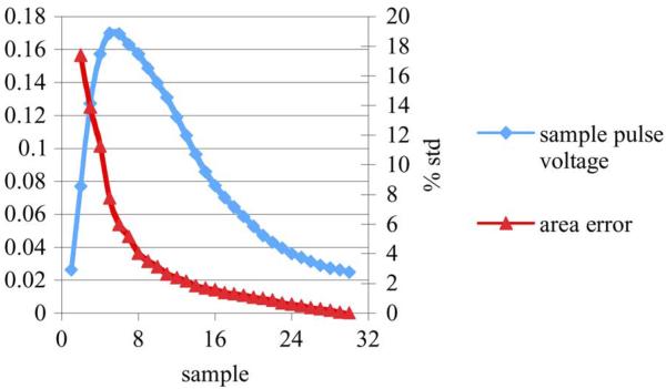
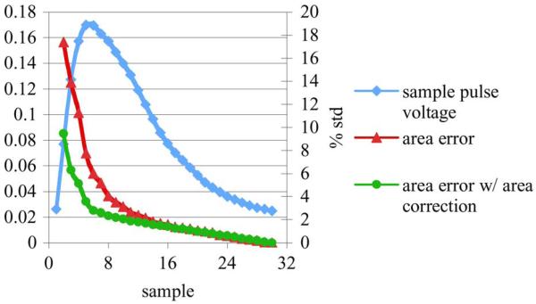
The next step is to determine how well the tail of the pulse can be interpolated based on summing up only a portion of the pulse. For this test, only one stream is needed. Again, for each percentage of pulse summed one thousand pulses were summed to the specified number of samples, while the rest of the pulse was interpolated with the reference pulse. In this case, the reference pulse was normalized to the data pulse. The resulting composite summation is compared to the summation of the total pulse. The percent standard deviation of the error for all 1000 pulses is plotted in Fig. 3, along with an example pulse. The percent standard deviation demonstrates how much overall error is associated with interpolating the tail. The area error increases as less of the pulse is summed and more is interpolated. Again, there is a dramatic increase in error at about the peak of the pulse.
Fig. 3.
Graph of area error as compared to how much of the pulse is interpolated for a 65 MHz sampled pulse.
The results in Figs. 2 and 3 indicate that about 20% (7 samples for a 65 MHz ADC) of the pulse is needed before the interpolation error becomes too great. In fact, for timing, the best results are obtained at about 30% of the pulse, and 20% is roughly equivalent to summing up the whole pulse. This is because the tail of the pulse contains a substantial amount of noise that corrupts the area normalization step. Given these results, the boundary that distinguished peak pile-up and tail pile-up is set to 20% of the pulse. That is, if pile-up occurs before 20% of the pulse, it should be detected and discarded. If it occurs afterwards, it can be separated with our algorithm. These results also indicate that there is not enough benefit to the complexity of truly dynamic integration. That is, integrate until a pile-up event is detected as is done in [11].
B. Area Correction
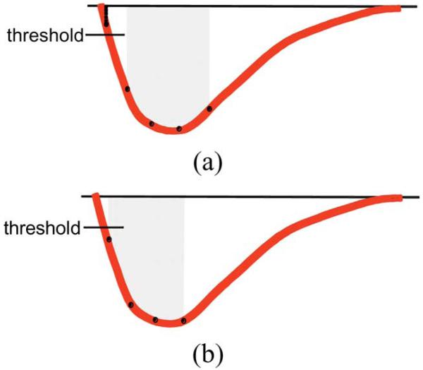
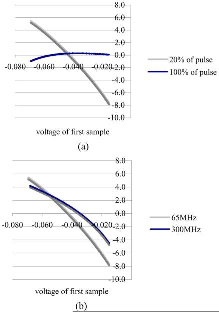
Even though the timing does improve as less and less of the pulse tail is summed for energy, there are some issues. One issue is the dependence of a pulse’s calculated energy on the voltage of the first sample (Fig.4). Since the number of samples summed is always the same, a sampling where the first sample is well above the threshold [Fig. 4(a)] will have a greater area than if the first sample was just above the trigger [Fig. 4(b)] for the same pulse.
Fig. 4.
Illustration of how the calculated area of the same pulse can differ based on the voltage of the first sample.
The range of possible voltages for the first sample of a pulse range from the voltage of the first trigger, to some greater value based on the slope of the leading edge and the sampling interval. A greater range and more variance in calculate areas of identical pulses will be seen with a longer sampling period and a steeper leading edge.
Fig. 5 shows the extent of this error. Each graph shows the difference between the average area of a pulse and the area calculated for the same pulse for a given first sample voltage, as indicated on the x-axis. The error is reported as a percent of the average pulse area for the amount of pulse summed. For example, Fig. 4(a) indicates that for a 65 MHz ADC, the area summation is almost 8% under estimated when the first sample is just above the threshold (−.015 V). There are no voltages below −.015 V because that is the voltage level of the trigger, so no samples will be below this value. Fig. 4(a) demonstrates how the error is worse as less of the pulse is summed for the area to amplitude normalization. Notice how percent error for summing up all of the pulse is nearly flat and centers around zero, while the error for summing up only 20% of the pulse has large errors when the first sample is at either end of the range. Fig. 4(b) shows how this error trends for different sampling rates. A higher sampling rate ADC means that there are more samples in the first 20% of the pulse, and the range of the first sample is less. This results in less error than a lower sampling rate. However, the improvement from 65 MHz to 300 MHz is not large because the slope of the leading edge of the 300 MHz-sampled pulse is greater because the frequency cutoff for the low-pass filter is higher. This is evident by the fact that the possible ranges of the first sample (x-axis) for both samplings is almost the same, though the range in time for the 300 MHz sampling ~ 1/5 that of the 65 MHz sampling.
Fig. 5.
Graphs indicating the area summation error based on the voltage of the first sample. (a) For a pulse sampled at 65 MHz while sampling 20% of the pulse or the whole pulse. (b) For a pulse sampled at 65 MHz and 300 MHz summing up 20% of the pulse.
To correct for this, the error shown in Fig. 5 is calculated using the reference pulse, and the correction is stored in a lookup table. The lookup table stores the difference between the average area of the reference pulse and the area obtained for the reference pulse given the voltage of the first sample. Recall that the reference pulse is defined at about every 60 ps so it has to be down sampled to match the ADC sampling period in order to accurately compare the reference pulse to the ADC data pulse. Based on the down sampling and the threshold, there is a theoretical range where the first sample can fall on the reference pulse. The lowest voltage is from a sample just above the threshold, and the largest voltage is when the previous sample is just below the threshold. The average area for the reference pulse is based on a sampling with the first sample is in the middle of this range.
Using the area correction value in the normalization step is an iterative process. The first sample that is used as the address to the look-up table has to be normalized first. So after the initial area of the first 20% of the pulse is calculated, the first sample of the pulse is normalized based on that area. The normalized voltage of the first sample is the address into the area correction lookup table, and the output is added to the initial area. Note that the normalized voltage of the first sample is not correct at this point, but it is close enough to use to look up the area correction value. The corrected area is used to normalize the first samples of the pulse again, which are used to determine the start time of the pulse. It is possible that this iterative process may need to be repeated more times for systems with larger area variances, but for this data set, one iteration sufficed.
The previous results, after correcting for the voltage of the first sample, are shown in Figs. 6 and 7. For both timing and area, there are no improvements when most of the pulse is summed, which is logical considering how flat the 100% summation line is in Fig. 5(a). The important difference in timing resolution and area error is when the summation limit approaches the peak of the pulse. For timing resolution in Fig. 6, correcting the area improves the timing at 20% summation by 6% and the standard deviation of the area interpretation reduces by 53%.
Fig. 6.
Graph of timing resolution versus amount of pulse summed with and without the area corrected for the amplitude of the first sample for a 65 MHz sampled pulse.
Fig. 7.
Graph of area error with and without area correction as compared to how much of the pulse is interpolated for a 65 MHz sampled pulse.
C. Peak Pile-Up Filter
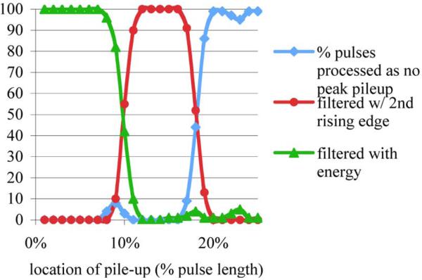
Determining whether a pile-up event has occurred before or after the 20% cutoff is calculated with the peak pile-up filter. Our implementation is composed of a two-part filter. The first part relies only on the energy of the first 20% of the pulse. If the signal in this region was too large, it is deduced that pile-up occurred before the cutoff and that the two pulses should be discarded as peak pile-up. This half of the solution is only as good as the energy resolution of the system though. This is because if the first pulse is on the lower end of the energy spectrum (or a result of Compton scatter), then more energy from a pile-up event (i.e., greater overlap) is required to trigger the filter. Therefore, if only this method was used many peak pile-up events would make it through the filter. The second part of the filter detects peak pile-up that occurs closer to the 20% cutoff. This is accomplished by looking for a second rising edge before the peak pile-up cutoff. This scheme relies on the fact that the location of the peak is fairly consistent. So, once the peak of a pulse is encountered (stored as a certain number of ADC samples) the filter looks for a number of samples that are greater than the peak value (but not necessarily increasing). The number of sample observed (for the second leading edge) is dependent on the ADC sampling rate. For a 65 MHz ADC, two samples are enough, but for a 1 GHz sampling, eight samples need to be compared so that small noise spikes do not trigger the filter incorrectly. The effectiveness of this two-part filter is shown in Fig. 8.
Fig. 8.
Plot of the peak filters ability to detect peak pile-up and percentage of peak pile-up filtered be each part of the filter.
Fig. 8 shows the results from a simulation to test this peak pile-up filter. The simulation was generated where 200 different pulses from the same pixel were put into a stream so that 100 2-pulse pile-up events were generated. The degree of pile-up for all 100 events was the same for each test. The pile-up started at 1% of the first pulse (essentially two pulses directly overlapping) and was swept to 25%. In other words, 25 tests were run with all of the 100 pile-up events having the same amount of pile-up. For each test, the peak pile-up detection scheme was run and the number of pulses that made it through the filter (did not detect peak pile-up) was noted, as well as how many pulses each part of the filter detected as peak pile-up. Ideally, the percentage of pulses processed as no peak pile-up would be 0% until pile-up at 20%, and then go immediately to 100% detected. Notice that the part that uses the energy in the first 20% of the pulse stops detecting peak pile-up when the second pulse is at about 13% of the first pulse. The reason for this is because some margin has to built in for the inaccuracy of calculating the energy of piled-up pulses. Fortunately, where the energy filters cuts off, the filter that looks for a second peak starts to detect peak pile-up. Before this point, the two peaks are close enough that the filter does not find a second rising edge. Notice that there is a slight bump in the number of pulses processed as tail pile-up around 10% because of the crossover between the two parts of the filter. Reducing the maximum energy value, at the cost of possibly filtering out some “good” pulses, can eliminate this bump.
D. Algorithm
From the previous tests, the algorithm for each engine is as follows:
remove baseline from incoming ADC stream (first engine only).
detect pulse based on triggers as discussed in [4].
sum up the first 20% and the whole pulse.
- check for peak pile-up with peak filter.
- if peak pile-up occurs disregard both pulses.
- otherwise continue.
normalize first sample of pulse based on area under first 20% of pulse.
calculate the area correction factor and adjust initial area.
normalize first samples (based on number of samples used in timing algorithm) of pulse to reference pulse using corrected area.
timestamp pulse as discussed in [4].
normalize reference pulse to data pulse using corrected area.
using timestamp, lookup the correct samples from the normalized reference pulse to interpolate remaining 80% of pulse tail.
subtract interpolated pulse from ADC stream and send resulting stream to second pile-up correction engine.
if downstream engine detects a pulse it repeats steps 2–11 on the pulse and the first engine uses the energy based on 20% summed plus 80% interpolated.
if no pulse is detected in the time it takes the first pulse to return to baseline, then the first engine uses the 100% summation for the pulse energy.
V. Results
To simulate the algorithm, 1000 pulses from four different pixels on a Zecotech MAPD-N array with a LFS-3 scintillator were captured using a 25 GHz oscilloscope. These pulses were then imported into Matlab to perform simulations. The pulses were captured as singles, and different percentages of pile-up and coincidence count rate were generated in Matlab before the above algorithm could be simulated. To facilitate this, two streams of pulses were created, with each stream composed of pulses from a single pixel. All pulses were randomly placed in the stream with a 50% coincidence rate. That is, when a pulse was randomly placed in stream one, it was randomly chosen with a 50% probability whether it would have a coincidental pair in stream two. In this work we investigate 100 kilocount per second (kcps), 200 kcps, 500 kcps, and 1 Mcps (below 100 kcps, pile-up is no longer a large issue, and 1 Mcps is greater than the count rate we expect to handle). The pile-up is generated when a random placement of a pulse overlaps an already placed pulse. In order to prevent the addition of two baseline components to a pile-up, the baseline was removed from the single pulses and added back to the whole stream after all of the pulses were places.
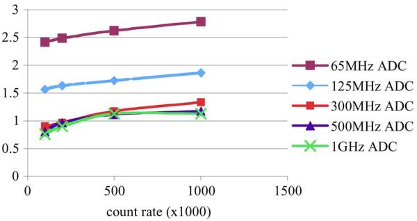
These streams were created with all possible unique pairings of the four pixels (six pairings), for five ADC sampling rates (65 MHz, 125 MHz, 300 MHz, 500 MHz, 1 GHz), and with four count rates (100 kcsp, 200 kcps, 500 kcps, 1 Mcps). The frequency cutoff of the filter was optimized to get as steep of leading edge while still maintaining at least three samples on it. The energy resolution and coincidence timing resolution was recorded for each test. The timing resolution was averaged over the six pixel pairings. The results for how timing resolution is affected by the count rate are shown in Fig. 9. As expected, the timing resolution improves as the ADC rates increase, and it degrades as the count rate increases because more pulses are involved in pile-up. The timing resolution from 100 kcps to 1 Mcps degrades by about 15% for a 65 MHz and 125 MHz sampling rate and about 40% for the other sampling rates. Notice that the degradation in terms of ns is similar for all sampling rates. This indicates that the timing resolution degradation is not dependent on the sampling rate. Fig. 9 also shows that our algorithm degrades gracefully as pile-up rates increase. As a reference, the timing resolution for these pulses without pile-up using a constant fraction discriminator is 850 ps.
Fig. 9.
Timing resolution for different count rates at different ADC sampling rates.
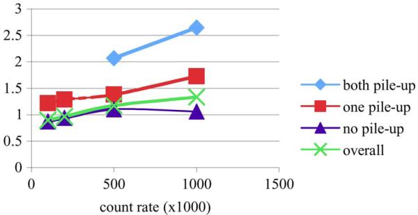
To get an understanding of what is contributing to the degradation, the timing resolution was calculated for each possible coincidence scenario. That is, coincidental pulses when neither pulse were involved in pile-up, when one of the two were in a pile-up event, and when both pulses were some part of a pile-up event. These results are presented in Fig. 10 for a 300 MHz ADC sampling rate, along with the overall timing resolution. Note that data for 100 kcps and 200 kcps for both involved in pile-up are missing. This is because there were not enough instances of those events at low count rates to make the data statistically sound.
Fig. 10.
Plot of timing resolution for a 300 MHz ADC sampling for different count rates. The timing resolution is shown for coincidental pulses where neither of the pulse is in a pile-up event, where one of the pulses is piled up and where both of the pulses were in a pile-up event.
Not surprisingly, it appears that most of the degradation is from the pile-up events, and especially from the case when both pulses in coincidence are involved in pile-up. More interestingly, there is still some degradation in the timing resolution for pulses not involved in pile-up when count rates increase. The degradation is about 17% from 100 kcps to 1 Mcps. This is probably due to the difficulty of calculating a good baseline when pulses are close together but not overlapped.
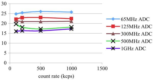
In addition to timing resolution, energy resolution is an important factor of a PET pulse processing system. For the pile-up correction algorithm, the energy resolution will give an indication of whether the energy of the pulses involved in pile-up can be accurately estimated. To calculate the energy resolution, the energy of all pulses in the stream (except those with too much pile-up) was recorded and a histogram was generated. The data set used in these experiments was for a point source in air. To determine the FWHM, a Gaussian function was fit to the data and the energy resolution was calculated. The results are reported in Fig. 11. Notice that the energy resolution is fairly constant over different count rates. In fact, the worst degradation from 100 kcps to 1 Mcps is less than 5%. The energy resolution is worse for lower sampling rates do to the discretization of the pulses.
Fig. 11.
Graph of the energy resolution of our pulse pile-up correction as count rates increase for different ADC sampling rates.
A. Pulse Detection
Since the purpose of pulse pile-up correction is to capture additional pulses, it is important to investigate pulse detection efficiency. That is, how well does the algorithm detect good pulses and reject peak pile-up pulses that have too much pile-up. To determine how well our algorithm is detecting pulses, statistics of pulse detection were kept as they were discovered and processed. Pulses were classified by the number of pulses in a given pile-up event. For example, 2-pulse pile-ups are events where two pulses piled up in a row, and 3-pulse pile-ups are events with three pulses in one pile-up. The number of pulses without pile-up, as well as pulses with peak pile-up was also reduced.
Analyzing our pile-up correction algorithm to determine the expected count rates is difficult because of the nature of the dead time. Recall that if pile-up occurs in the first 20% of a pulse, then the system is dead until the incoming ADC values return to baseline. So, if a third pulse arrives before the system returns to baseline, then the dead time is extended by another pulse length. So, our system has essentially two dead times. The dead time when the system is live (not resolving peak pile-up) is 20% of the length of a pulse. That is, when the system is live, the minimum separation required between two pulses is 20% of the pulse length. When peak pile-up does occur, the dead time is then the full pulse length. The system is dead for at least one pulse length until the data stream returns to baseline. Given these parameters, the pile-up rates cannot be calculated with the typical statistical models that assume a single dead time, so instead the pile-up rates were calculated with a Monte Carlo simulation.
Specifically, the rates were tabulated from the stream generation routine. After each stream was generated, the start times of every pulse were evaluated to determine how many pulse “groups” had no pile-up, and how many were a 2-pile-up, 3-pile-up or 4-pile-up event. The occurrence of peak pile-up was also determined. The results in Table I show the percent difference from detected to expected for each subcategory.
TABLE I.
Percent Differences From Detected Pile-Up Events to Expected Pile-Up Events (Detected Count/Expected Count)
| count rate |
no pile-up |
2-pulse pile-up |
3-pulse pile-up |
4-pulse pile-up |
peak pile-up |
|---|---|---|---|---|---|
| 500kcsp | (1702/1706) −.2% |
(113/107) 5.3% |
(5/4) 20% |
(0/0) 0% |
(32/42) 23.8% |
| l Mcps | (1442/1455) −.9% |
(169/170) −.6% |
(17/23) −35.3% |
(8/4) 50% |
(56/69) 18.8% |
Notice that this algorithm does a good job at correctly finding pile-up. The slight difference is mostly due to the way the expected pile-up rates were calculated versus the detected rates. The expected rates used the pulse length to determine if a pile-up occurred based on the start times of pulses. The pulse length is the same value for all pulses from a single pixel for implementation simplicity, even though the pulses do vary in length in practice. Additionally, the stored pulse length is slightly less than it takes for the pulse to return to baseline for other issues. The algorithm on the other hand looks for a second pulse before the current pulse has decayed back to baseline. So even if the pulse length has expired, a pileup may be detected because the stream had not returned to baseline yet. This is why more pile-up events were detected, but fewer no pile-up events.
VI. FPGA Implementation
This algorithm was specifically designed for an efficient FPGA implementation, targeted towards our second-generation hardware [1]. The goals for an efficient implementation are low logic and memory utilization and real-time computation. Minimal logic utilization is required to reduce power consumption and to accommodate the other pulse processing circuits present in the FPGA, as well for multiple channel support. The real-time criteria is important because we do not want to add dead time to the system.
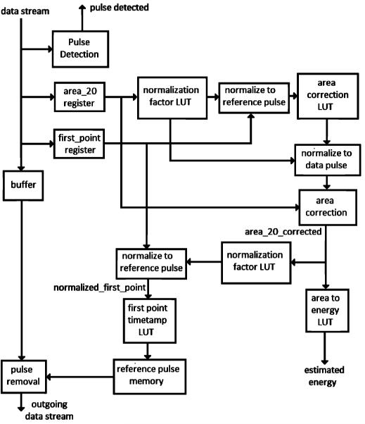
The FPGA implementation of this algorithm is built on the timing algorithm discussed in [4]. The first change required is in the area-to-amplitude normalization step. The contents of this lookup table were modified to operate on the first 20% of the pulse rather than the entire pulse. Another addition is the area correction factor, which can be implemented as a lookup table. The final addition is the system that interpolates the tail and subtracts it from the stream. The block diagram for one pulse pile-up correction engine is shown in Fig. 12. The number of engines is user-selected according to the count rate and the desired amount of pile-up correction.
Fig. 12.
Block diagram of one pulse pile-up correction engine.
Most of these new logic blocks are standard logic designs. The primary challenges in this design are related to the latency through the engine. The first issue has to do with the control of the overall system. In the preliminary implementation, a master control block listened to each engine to determine when the first engine should process the stream, or when another engine is processing pile-up. This was important because the first engine should trigger only on the first pulse of a pile-up event. The problem with this control scheme is the latency through all of the engines. In other words, if it takes N cycles for a sample from the ADC to get through an engine, then the first engine will miss a multiple N samples from the ADC (depending on the number of engines). To correct this, each engine independently waits for the incoming samples to return to baseline after it has processed a pulse. The downstream engine must notify the upstream engine of any pulses it detects so that the upstream engine can determine whether to use the pulse energy from summing all of the samples or the energy from interpolating the tail. This scheme does require a simple termination engine after the final engine, to provide this information.
The other issue around latency is the coarse coincidence calculation. In our system [2], we utilize a coarse coincidence controller to lower the data rate to the host computer. The coarse coincidence controller is a separate FPGA that listens for events from all detectors and indicates when two events occurred in the field-of-view within the three-clock cycle coarse coincidence window. The problem occurs when two coincidental pulses are not in the same place of the pile-up stream. For example, if a single pulse was in coincidence with the second pulse of a pile-up event, the event signal for the single pulse would arrive at the coincidence controller N cycles before the other event due to the latency through the pulse pile-up correction engines. This is corrected by delaying the pulse signal to the coarse coincidence controller from all of the engines except the last. The second-to-last engine has a delay of N, while the next engine upstream has a delay of 2N, and so on.
This algorithm was implemented in Verilog and compiled with Quartus for the StratixIII S200 FPGA used in our hardware. Each engine utilizes 217 LUTs (.1%), 337 284 memory bits (3.2%) and 6 DSP blocks (1%). The termination engine only uses 8 LUTs and 24 memory bits. Duplicating pile-up engines will not necessarily double the resources used. Some of the memories can be shared between two engines by utilizing the dual ports on the FPGA block memories. For a system with two pulse pile-up correction engines, the memory usage is 552 592 bits. This represents a savings of 18% over simply duplicating the memory. There is also some possible memory savings by reducing the resolution of the reference pulse by down sampling it. This would require further study to determine the effect on timing and energy resolution.
VII. Conclusion
In this work, we show that an all-digital pulse pile-up correction algorithm can reliably recover pulses overlapped up to 80%. This allows systems to process higher count rates from higher tracer dosages or from architectures that have higher count rates per channel. Simulation for 1 Mcps show that this algorithm is able to capture and process 30% more pulses than if all pile-up was simply discarded. The timing resolution does degrade by 40% when utilizing this algorithm however, but the timing resolution degrades by 10% (100 kcps) to 80% (1 Mcps) if no correction or detection is done at all on the pile-up streams. Finally, this algorithm ties in very well with our timing algorithm [4] and can easily be implemented in an FPGA with a reasonable amount of resources.
Acknowledgments
This work was supported in part by DOE grant DE-FG02-05ER15709, Zecotech, Altera, and NIH grant EB002117.
Footnotes
Color versions of one or more of the figures in this paper are available online at http://ieeexplore.ieee.org.
Contributor Information
M. D. Haselman, Sandia National Labratories, Livermore, CA 94550 USA (mhaselm@sandia.gov)
J. Pasko, Department of Electrical Engineering, University of Washington, Seattle, WA 98195 USA (jpasko@ee.washington.edu)
S. Hauck, Department of Electrical Engineering, University of Washington, Seattle, WA 98195 USA (hauck@ee.washington.edu).
T. K. Lewellen, Department of Radiology, University of Washington, Seattle, WA 98195 USA (tkldog@u.washington.edu).
R. S. Miyaoka, Department of Radiology, University of Washington, Seattle, WA 98195 USA (rmiyaoka@u.washington.edu).
REFERENCES
- [1].Lewellen TK, et al. Design of a second generation firewire based data acquisition system for small animal PET scanners; IEEE Nuclear Science Symp. Conf. Record; 2008; pp. 5023–5028. [DOI] [PMC free article] [PubMed] [Google Scholar]
- [2].Lewellen TK, Janes M, Miyaoka RS, Gillespie SB, Park B, Lee KS, Kinahan P. System integration of the MiCES small animal PET scanner; IEEE Nuclear Science Symp. Conf. Record; 2004.pp. 3316–3320. [Google Scholar]
- [3].DeWitt D, Miyaoka RS, Li X, and C. Lockhart,, Lewellen TK. Design of a FPGA based algorithm for real-time solutions of statistics-based positioning; IEEE Nuclear Science Symp. Conf. Record; 2008; pp. 5029–5035. [DOI] [PMC free article] [PubMed] [Google Scholar]
- [4].Haselman MD, Hauck S, Lewellen TK, Miyaoka RS. Simulation of algorithms for pulse timing in FPGAs; IEEE Nuclear Science Symp. Conf. Record; 2007; pp. 3161–3165. [DOI] [PMC free article] [PubMed] [Google Scholar]
- [5].Haselman M, Hauck S, Lewellen TK, Miyaoka RS. FPGA-based pulse parameter discovery for positron emission tomography; IEEE Nuclear Science Symp. Conf. Record; 2009; pp. 2956–2961. [DOI] [PMC free article] [PubMed] [Google Scholar]
- [6].Miyaoka RS, Li X, Lockhart C, Lewellen TK. New continuous miniature crystal element (cMiCE) detector geometries; IEEE Nuclear Science Symp. Conf. Record; 2009; pp. 3639–3642. [DOI] [PMC free article] [PubMed] [Google Scholar]
- [7].Shih YC, et al. An 8 × 8 row-column summing readout electronics for preclinical positron emission tomography scanners; IEEE Nuclear Science Symp. Conf. Record; 2009; pp. 2376–2380. [DOI] [PMC free article] [PubMed] [Google Scholar]
- [8].Lewellen TK, Bice AN, Pollard KR, Zhu JB, Plunkett ME. Evaluation of a clinical scintillation camera with pulse tail extrapolation electronics. J. Nucl. Med. 1989;30:1544–1558. [PubMed] [Google Scholar]
- [9].Wong WH, Li H. A scintillation detector signal processing technique with active pile-up prevention for extending scintillation count rates. IEEE Trans. Nucl. Med. 1998;45(3):838–842. [Google Scholar]
- [10].Liu J, et al. Real time digital implementation of the high-yield-pile-up-event-recovery (HYPER) method; 2007 IEEE Nuclear Science Symposium Conference Record.pp. 4230–4232. [Google Scholar]
- [11].Nakhostin M, Podolyak Z, Regan PH, Walker PM. A digital method for separation and reconstruction of pile-up events in germanium detectors. Rev. Sci. Instrum. 2010;81(10) doi: 10.1063/1.3499241. [DOI] [PubMed] [Google Scholar]
- [12].Tambave G, Guliyev E, Kavatsyuk M, Schreuder F, Löhner H. Pulse pile-up recovery for the front-end electronics of the PANDA electromagnetic calorimeter; IEEE Nuclear Science Symp. Conf. Record; 2011.pp. 2163–2168. [Google Scholar]
- [13].Arseneau RE. Method and Apparatus for Unpiling Pulses Generated by Piled-Up Scintillation Events. U.S. Patent 5 210 423. 1993 May 11;


