Abstract
We have developed arrays of nanomechanical systems (NEMS) by large-scale integration, comprising thousands of individual nanoresonators with densities of up to 6 million NEMS per square centimeter. The individual NEMS devices are electrically coupled using a combined series-parallel configuration that is extremely robust with respect to lithographical defects and mechanical or electrostatic-discharge damage. Given the large number of connected nanoresonators, the arrays are able to handle extremely high input powers (>1 W per array, corresponding to <1 mW per nanoresonator) without excessive heating or deterioration of resonance response. We demonstrate the utility of integrated NEMS arrays as high-performance chemical vapor sensors, detecting a part-per-billion concentration of a chemical warfare simulant within only a 2 s exposure period.
Keywords: NEMS arrays, gas chromatography, gas detectors, mass sensing
In the last several years, individual nanoelectromechanical resonators have been used to establish record sensitivities in force,1 position,2 mass,3,4 and gas concentration.5 The miniscule size of nanomechanical systems (NEMS) sensors clearly gives them unprecedented sensitivity to external perturbations, but this sometimes comes at a cost. For example, the power these devices can use and the magnitude of signal they can produce both decrease at smaller sizes. Moreover for gas sensors, the interaction cross-section with particular analytes in a gas or liquid environment can rapidly decrease as the active mechanical element becomes smaller, whether due to increased analyte diffusion time, interaction with nonactive sensor regions, or noisy, stochastic absorption/desorption of trace analyte levels.6 In this limit of “needle in a haystack” detection, individual NEMS may have difficulty capturing even a single molecule of the analyte. Such challenges can make it difficult to exploit the full potential of individual NEMS sensors in the next generation of real-world microanalytical tools.
It is therefore critical to scale up the interaction cross-section of NEMS sensors while still maintaining, or even enhancing, their extraordinary sensitivities and useful attributes. A straightforward and commonly used approach to this task is simply to combine individual devices into arrays. For chemical sensors, different devices within the array can serve as sensors of different chemical compounds. Such arrays have previously been fabricated from microscale cantilever resonators,7 microscale membrane resonators,8 nanoscale cantilevers,9 nanoscale doubly clamped beam resonators,10 and nanowire resonators.11 Alternatively, one can use the collective response of multiple elements of the array to enhance the signal-to-noise ratio or other properties. For example, by engineering the mechanical coupling between individual resonators, one can produce a collective mode of oscillation that inherits the positive characteristics of individual resonators, such as high frequency and quality factor, but is able to handle more power.12 Such collective modes can then be further optimized to produce the desired overall response, for example, that of a bandpass filter.13
In this paper, we report the first application of large-scale-integrated (LSI) fabrication techniques to NEMS array fabrication, which has allowed us to utilize the collective response of thousands of NEMS resonators to enable new paradigms in NEMS-based sensing. For our first realization of a LSI-NEMS sensor, we take an approach that requires a highly uniform array of nearly identical submicrometer-scale elements over a much larger (millimeter-scale) area. Our design relies on the essentially coherent response of thousands of independent resonators, connected electrically in a manner that provides natural noise averaging, increased collective power handling capability, and fault-tolerant robustness. LSI-NEMS arrays, while dramatically increasing the interaction cross-section of individual NEMS resonators, furthermore provide a potential route to orders-of-magnitude sensitivity improvements over individual resonator elements. As a proof-of-design, we demonstrate parts-per-billion sensing of the chemical warfare agent simulant diisomethylphosphonate (DIMP) within a 2 s exposure window using a functionalized LSI-NEMS.
Our NEMS arrays were fabricated from CMOS-compatible materials using state-of-the-art microelectronic lithography and etching techniques. The devices were fabricated on 200 mm SOI wafers with a 160 nm-thick silicon layer and a 400 nm thick buried oxide layer. A 70 nm-thick film of aluminum silicide14 was sputtered on top of the SOI wafer and patterned using 248 nm deep-UV lithography. Anisotropic etching of the thin metal film was then used to define the self-sensing piezoresistive elements of the NEMS array itself as well as the lead wires and the wirebonding pads.5 This patterned metallization layer also served as a mask for the anisotropic etching of the structural silicon layer down to the buried oxide. Finally, the NEMS cantilevers were released using a carefully timed vapor HF etch of the buried oxide. The details of the fabrication procedure are described in the Supporting Information.
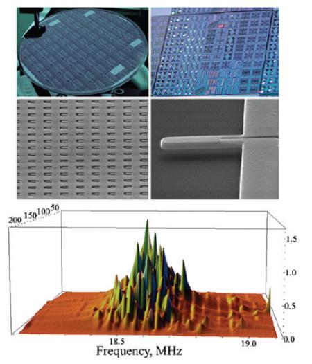
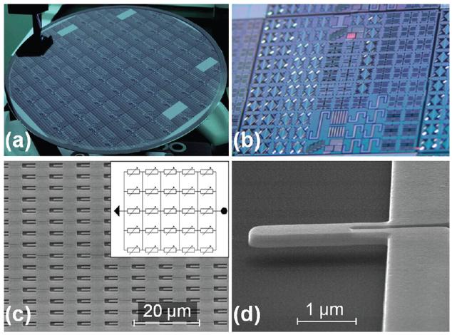
Figure 1 shows a completed 200 mm wafer of LSI-NEMS arrays, as well as a representative array and an individual cantilever element. Arrays were fabricated with different individual NEMS element dimensions across the wafer with the lengths varying between 1.6 and 5 μm, and the widths varying between 800 nm and 1.2 μm. A typical array contained 20 rows and 140 columns with a 6.5 μm linear pitch for a total of 2800 array elements. The largest arrays employed in the present work contained 6800 NEMS with an integration density of nearly 6 million NEMS per square cm.
Figure 1.
(a) Photograph of a full 200 mm wafer with patterned NEMS arrays. (b) Zoomed-in photograph of one 20 mm wafer die containing a variety of nanofabricated resonator array structures. (c) Scanning electron micrograph of a section of a cantilever array. Inset: Schematic of a combined series-parallel electrical connection of array elements. (d) Scanning electron micrograph (oblique view) of an individual array component.
A straightforward approach to harnessing the power of many individual NEMS in large-area arrays is to connect them electrically in a combined series-parallel configuration, shown in the inset of Figure 1c. A single-port (signal and ground) connection to the array can then be made through electrodes on opposite edges of the array. The individual NEMS were excited into vibration using electrothermally generated strain,15 which allowed us to actuate each array element with essentially identical driving phases. This phase coherence is critical for harnessing the collective benefits of the array geometry (see Supporting Information) and cannot be easily achieved with off-chip actuation methods. For example, piezoshaker actuation suffered from large phase lags due to propagation and interference of acoustic waves across the full extent of the millimeter-scale array. Since electric signals propagate at close to speed of light, rather than speed of sound, purely electric actuation, such as the thermoelastic mechanism, provides much more coherent driving signal to all array elements.
The resulting motion was detected electrically through the metal surface layer’s piezoresistive response.16 Details of the actuation and detection circuitry are in the Supporting Information. The most immediately apparent benefits of this configuration are the simplicity of electrical connection and the high degree of robustness with respect to lithographic defects and mechanical or electrical damage. Arrays of this type can be used as sensors even if most individual cantilevers prove defective, as long as there remains a conductive path through the array. In addition, the arrays of the series-parallel connected cantilevers are highly resistant to electrostatic discharge (ESD) because of their much larger collective power handling ability.
Another potential benefit of LSI piezoresistive NEMS sensor arrays emerges when we consider how the measured response of the entire array, that is, the change in overall resistance, relates to the changes in resistance of the individual array elements. Assuming for simplicity that all cantilevers have the same at-rest resistance, r, and that the fractional variations in the resistance of individual cantilevers are small, it is easy to derive that the relative change in the resistance of the array is the average of the relative change in the resistance of individual array elements (see Supporting Information for details)
| (1) |
where Δrij is the change of the resistance of the cantilever situated in the ith row and jth column of the array and N = lm is total number of array elements. The resistance contribution from each resonator Δrij will be a combination of mechanical signal and aggregate noise (e.g., Johnson noise, phase noise, thermal fluctuation noise).17 However, if every element of the NEMS array is identical, that is, if all element signals are at the same frequency and phase, then signal and noise do not add similarly in eq 1. In essence, the mechanical signals will sum coherently, while many of the individual resonator noise contributions add together incoherently. A full analysis (see Supporting Information) shows that, in the ideal case of identical resonators driven at the same frequency and phase, the signal-to-noise ratio scales as the square root of the number of array elements. For arrays comprised of thousands of elements, this can potentially result in orders of magnitude improvement in SNR for NEMS arrays vs single NEMS.
In practice, it is of course impossible to realize the ideal LSI NEMS array, since it would require zero process variations over the large area of the array. However, as we detail in the Supporting Information, achieving reasonably high (albeit imperfect) frequency uniformity can still yield enhanced SNR over that of single resonators. The frequency response of such an array can then be approximately described by a Lorentzian, just like in the case a single driven harmonic oscillator. However, the effective quality factor, Qeff, of the array response is set by both the individual element quality factor, Q, and the width of the resonance frequency distribution, Δf, of the array. To wit, Qeff ≈ 1/(Q−1 + Qdistr−1), where Qdistr ≈ f/Δf describes the relative magnitude of resonance frequency dispersion across the array. In our arrays, the dispersion of resonance frequencies across the array was of the order of 1%, corresponding to Qdistr ≈ 100.
Since the absolute size of typical lithographic and etching imperfections does not depend on the dimensions of the cantilever, the relative frequency dispersion decreases (Qdistr increases) with increasing cantilever length. However, the quality factor of individual cantilevers in air, Qair, generally increases with resonance frequency and therefore decreases with increasing cantilever length.18 As a result, there is some optimal cantilever length, for which the Qdistr ≈ Qair, and Qeff ≈ Qdistr/2 ≈ Qair/2. While we have studied arrays of various dimensions, we obtained optimal results from arrays made out of 2 μm long, 800 nm wide cantilevers, whose individual resonance frequencies were approximately 24 MHz. The quality factors of such individual cantilevers in vacuum and air were on the orders of 1000 and 100, respectively. In vacuum, the overall observed array response was thus largely determined by the frequency dispersion, Qeff,vac ≈ Qdistr ≈ 100; whereas in air the trade-off was close to optimal: Qair ≈ Qdistr ≈ 100 and Qeff,air ≈ (1/Qair +1/ Qdistr)−1 ≈ 50.
The motion of the array cantilevers was actuated thermoelastically and detected piezoresistively using the two-port downmixing measurement scheme described in the Supporting Information. In the two-port scheme, a single metal loop on a resonator is used for both thermoelastic actuation and piezoresistive detection. This measurement scheme worked in the same way for arrays as for individual cantilevers, the only difference being the need to supply more RF power. To further maximize the resonance signal visibility, we measured two arrays at the same time using the balanced differential scheme.19
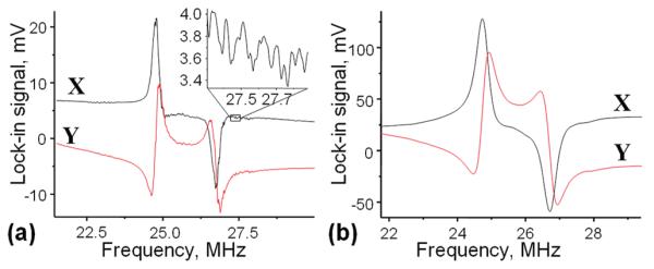
In the balanced measurement technique, the two arrays must have different center frequencies but similar overall resistances. In that case, the coherent backgrounds generated in each of the arrays cancel each other, but the resonance responses do not because the resonances occur at different frequencies for the two arrays. Figure 2a shows a typical resonance response measured in vacuum using two arrays with cantilevers of nominal lengths of 2.0 and 2.1 μm. The graph features two resonance peaks with the lower-frequency one corresponding to the array with longer cantilevers and vice versa.
Figure 2.
(a) Resonant response of the two arrays in vacuum. Both quadratures of the lock-in response, X and Y, are shown. The inset shows a zoomed-in version of a part of the measured response curve. Note that the noise level in these measurements was more than an order of magnitude smaller than the amplitude of the rapid variations shown in the inset. (b) Same for measurements in air. Note that the amplitudes of the resonance peaks were much larger than in (a) because much more RF power was applied to drive and detect the resonances in air.
Note that the vacuum response curves featured many sharp features that are caused by the individual resonances of cantilevers whose frequency lied outside the majority of resonance peaks of the array. These features were reproducible and larger than the amplitude of measurement noise by approximately 2 orders of magnitude. According to theory, the individual resonances should be smaller than the overall peak by a factor of N × Qeff/Q ≈ 2800(100/1000) = 280. However, we found the sharp features to be approximately 100 times smaller than the overall peak, suggesting that they are not individual resonances but rather superpositions of several resonances. In air, these variations were smoothed out, as shown in Figure 2b.
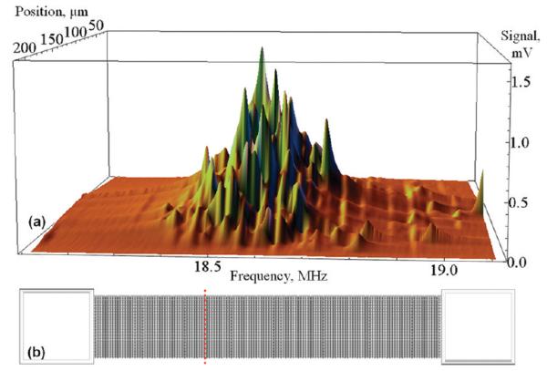
To further study the dispersion of frequencies in the arrays, we have also done measurements using thermoelastic actuation and optical detection in vacuum. The optical detection setup was a simple reflection interferometer with a spot size of approximately 10 μm, previously used in ref 20. The results are shown in Figure 3, where we plot the interferometer signal of an array of 2.8 μm long, 1.2 μm wide cantilevers versus excitation frequency and the position of the beam spot. The position of the beam spot was stepped every 5 μm across the width of an array (see Figure 3b).
Figure 3.
Optically detected spectrum of cantilevers in a representative array for different positions of the laser spot (spot size approximately 10 μm). (b) Top-view schematic of a 140 × 20 array of cantilevers. Individual cantilevers are not visible in this image. The dotted red line schematically shows the positions of the laser spot used to acquire the spectra.
The small size of the optical spot allowed us to detect only about a dozen cantilevers within the beam spot instead of the entire array of 2800 cantilevers. The majority of individual resonances were situated near the central frequency of 18.6 MHz, and these resonances formed the main peak of the array response. Similar to electrical data on other arrays, however, there were also a number of “outliers”, especially at frequencies above the central peak. Some of these resonances were sufficiently well resolved to be fitted individually. The quality factor of such individual resonances in vacuum was approximately 1100.
One of the main advantages of NEMS arrays over individual devices is the much improved power matching and collective power handling capability. Since the total resistance of the array consisting of l rows and m columns is given by (mr)/l, it is possible to produce impedance-matched arrays from a wide range of individual resonators simply by changing the row and column count. The individual cantilevers that we used to build arrays had typical resistances of approximately 7 Ohms, so that 20 × 140 arrays we typically used had total resistances of 7Ω × 140/20 ≈ 50 Ω, which were optimally matched to commercial power electronics.
Apart from easy power matching, NEMS arrays have dramatically increased collective power handling capabilities compared to individual devices. As a rule of thumb, arrays can handle powers that are larger by a factor of N, the total number of array elements. While individual devices of the dimensions that we used typically had a maximum power handling ability of less than one milliwatt, our arrays could easily handle maximum powers of a few watts. For example, the collective RF power applied to the two arrays in the balanced measurement scheme was 900 mW per array for the data shown in Figure 2b. Applying even higher RF power of approximately 2 W per array produced significant frequency drift but no permanent damage to the arrays. This suggests that even higher power levels can be used with improved heat sinking at the die level.
The primary goal of developing the cantilever arrays described in this work was to create sensors that are more robust, easier to use, and potentially more sensitive than individual devices. One sensor application where arrays can offer large improvements is gas sensing and, in particular, NEMS-based gas chromatography.9 In this application, the sensor arrays need to be integrated with the gas delivery system. In prior work from our group, this was accomplished by encapsulating the nanomechanical sensor in a microfluidic flow cell that could then be directly connected to an external gas delivery system, such as a commercial gas chromatography (GC) system.9 This way, the nanoscale resonator is only exposed to the analytes and carrier gas and remains isolated from the air of the environment. In addition, the volume of the cell and, therefore, the diffusion time, which often limits the speed of gas chromatography analysis, can be minimized with proper design.9
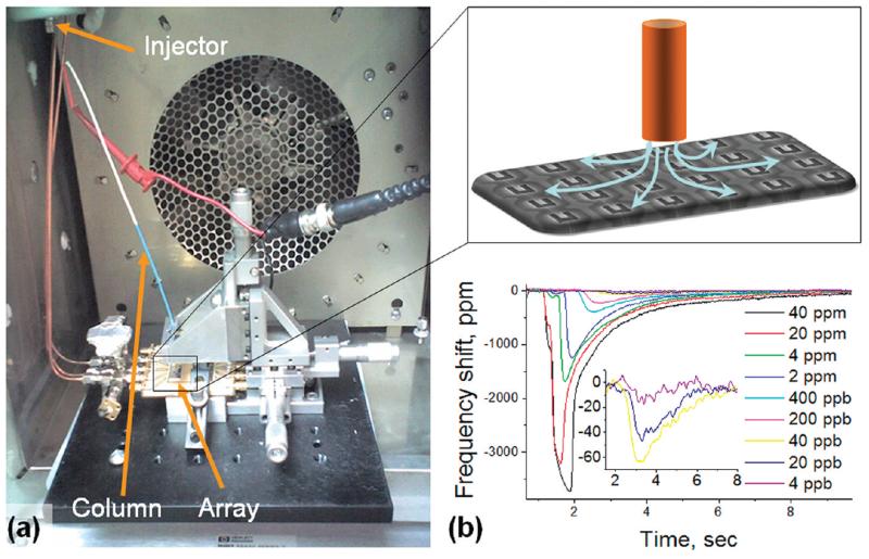
In this work, we did not use a microfluidic cell but instead operated the arrays in ambient air and used a micropositioner to move the end of the 90 cm long column of the gas chromatography system approximately 100–200 μm above the sensor array (Figure 4a). While not appropriate for industrial applications, this simple configuration allowed rapid device testing and did not result in increased diffusion time compared to the microfluidic cell experiments.11 To demonstrate the possibility of using arrays for detection of specific analytes, we coated the arrays with the polymer DKAP, a silicone copolymer developed at Sandia National Laboratory for detection of phosphonate gas molecules—precursors and simulants of nerve gas agents.21,22 A droplet of DKAP solution was put on the array chip surface and left to dry in air, leaving a thin (10–20 nm) film of polymer on the array cantilevers.
Figure 4.
(a) Integration of the array sensors into a commercial Hewlett-Packard 5890 gas chromatography system. The photograph shows the inner chamber of the GC system with the injector, column, and column heating wires as well as the printed circuit board with the sensor arrays and a micropositioner. The inset shows schematically how the lower end of the column is positioned above the array and how the effluent flows from the column. (b) Gas chromatogram of DIMP obtained with an array sensor in the bridge configuration with 10 W resistive heating of the 90 cm long column. The inset shows zoomed-in versions of the chromatograms for the lowest DIMP concentrations. The averaging time was 150 ms in these measurements, corresponding to a bandwidth of 1/(2π × 0.15 s) ≈ 1 Hz. The rms amplitude of noise corresponds to a frequency shift of 3 ppm and therefore a concentration sensitivity of approximately 1.2 ppb. The total RF power used in these measurements was approximately 360 mW per array.
Functionalization of the array did not have a measurable effect on the frequency or the effective quality factor of the array response. However, the quality factor was noticeably affected by the flow of the hydrogen carrier gas through the column. When the GC system was in operation, the hydrogen carrier gas was forced out of the bottom end of the column at the rate of 1–2 sccm (standard cubic centimeters per minute) and largely displaced the air in the immediate vicinity of the array (see inset of Figure 4a). Because the viscosity of hydrogen is lower than that of air, this increased the quality factor of individual resonances, Q, and therefore the effective quality factor of the entire array in accordance with the formula Qeff = 1/(Q−1 + Qdistr−1). In practice, the effective quality factor typically increased from approximately 50 to approximately 60.
In order to test the gas sensing functionality of the arrays, we have performed open-loop measurements of frequency shift of the array sensor after injecting solutions of diisopropyl methylphosphonate (DIMP), a nerve gas simulant, in CS2 solvent through a GC column as described above. The open-loop frequency measurements of frequency shift were carried out by monitoring the dispersive quadrature of the Lorentzian response (see, for example, curve Y in Figure 2b). If the drive and bias frequencies remain constant and the central peak frequency of the arrays ωR changes by ΔωR due to an absorbed mass Δm, the dispersive components of the resonance voltage signal will change by
| (2) |
where Aarr is the voltage amplitude of the array resonance peak, and mc is the mass of the cantilever. Therefore, as long as the total frequency shift is smaller than the resonance width, we can easily infer the changes in the resonance frequency from the measured changes in the dispersive quadrature of the signal.
Figure 4b shows the resulting chromatograms for a wide range of DIMP mass injections. The downward shift in the frequency response of the array was caused by the uptake of DIMP molecules by the DKAP polymer that covered the cantilevers as the chemical was eluted from the open end of the GC column. The total observed frequency shift did not exceed 0.4% << 1/Qeff ≈ 2%, ensuring a linear relationship between the measured dispersive component and the loading mass.
The resulting average concentrations c in the eluted peaks are calculated as9 c = (clVlVmSR)/(MWFΔt), where cl is the mass density of DIMP in the liquid sample, Vl is the liquid volume of sample injected into the column, Vm = 22.4 L/mol is the molar volume of an ideal gas at ambient temperature and pressure, SR is the injection split ratio, MW is the molecular weight of the analyte, Δt is the peak width in time, and F is the column flow rate.
At large concentrations (above 1 ppm), the frequency shift peak area did not follow a linear relationship with the concentration of DIMP due to saturation of the polymer film. The response was more linear at smaller concentrations, with both the shape and the delay of the peak independent of the DIMP concentration (see inset to Figure 4b). The data demonstrate a minimum detectable concentration of approximately 1.2 ppb in a 1 Hz bandwidth, which is roughly optimal for detecting short-column pulses a few seconds in length. This limit does not surpass the minimum equilibrium sensitivity that was demonstrated in our group for individual NEMS cantilevers using long columns and averaging times,9 but it improves upon the short-term sensitivity of individual devices in that work, which were obtained using similar high-speed GC measurements with pulse lengths of only a few seconds. We are currently verifying whether this sensitivity improvement is fully explained by the array’s improved signal-to-noise ratio and active surface area, or is also due to the different measurement geometries.
We conclude by noting some of the further possibilities enabled by developing NEMS technology compatible with LSI fabrication techniques. For example, our process for fabricating NEMS arrays is completely amenable to integration with the CMOS electronics needed to drive and detect the resonances of NEMS devices. In the future, such integration will allow us to fabricate arrays of independently operating nanomechanical oscillators (as opposed to resonators). Such oscillators will be needed in extremely low analyte concentration regimes (parts-per-quadrillion and below), where the number of interacting molecules per individual NEMS approach one and collective averaging no longer improves the SNR. Such oscillators should also prove useful for NEMS-based mass spectroscopy,3 as well as a new test bed for studying nonlinearly interacting oscillators. Furthermore, it may be possible to incorporate low-power actuation and detection techniques into arrays. In particular, piezoelectric detection and actuation should allow more efficient transduction of RF power into mechanical motion of NEMS arrays. Piezoelectric detection on the array level would also avoid the problem of signal shorting by parasitic capacitances, which generally prevents the use of piezoelectric detection in individual NEMS devices. The use of piezoelectric actuation would also dramatically reduce the total power dissipation of NEMS arrays without reducing their power handling capability, thereby improving the overall power efficiency of NEMS array sensors.
Supplementary Material
ACKNOWLEDGMENTS
The authors thank R. Karabalin for help with optical measurements. We gratefully acknowledge support from the Defense Advanced Research Projects Agency via DARPA/MTO-MGA Grant NBCH1050001, as well as support from the Institut Carnot via the Carnot-NEMS project.
Footnotes
Supporting Information
A description of the fabrication procedure and measurement circuit, as well as a more detailed analysis of series-parallel piezoresistive NEMS detection, is provided. This material is available free of charge via the Internet at http://pubs.acs.org.
REFERENCES
- (1).Rugar D, Budakian R, Mamin HJ, Chui BW. Nature. 2004;430:329–332. doi: 10.1038/nature02658. [DOI] [PubMed] [Google Scholar]
- (2).LaHaye MD, Buu O, Camarota B, Schwab KC. Science. 2004;304:74–77. doi: 10.1126/science.1094419. [DOI] [PubMed] [Google Scholar]
- (3).Naik AK, Hanay MS, Hiebert WK, Feng XL, Roukes ML. Nat. Nanotechnol. 2009;4:445–450. doi: 10.1038/nnano.2009.152. [DOI] [PMC free article] [PubMed] [Google Scholar]
- (4).Jensen K, Kim K, Zettle A. Nat. Nanotechnol. 2008;9:533–537. doi: 10.1038/nnano.2008.200. [DOI] [PubMed] [Google Scholar]
- (5).Li M, Tang HX, Roukes ML. Nat. Nanotechnol. 2007;2:114–120. doi: 10.1038/nnano.2006.208. [DOI] [PubMed] [Google Scholar]
- (6).Arlett J, Myers EB, Roukes ML. Nat. Nanotechnol. 2007;6:203–15. doi: 10.1038/nnano.2011.44. [DOI] [PMC free article] [PubMed] [Google Scholar]
- (7).Zhang Z, Lang HP, Huber F, Bietsch A, Grange W, Certa U, McKendry R, Gunterodt H-J, Hegner M, Gerber Ch. Nat. Nanotechnol. 2006;1:214–220. doi: 10.1038/nnano.2006.134. [DOI] [PubMed] [Google Scholar]
- (8).Lee HJ, Park KK, Kupnik M, Oralkan Ö, Khuri-Yakub BT. Proc. IEEE Sensors Conf. 2010:2122–2126. [Google Scholar]
- (9).Li M, Myers EB, Tang HX, Aldridge SJ, McCaig HC, Whiting JJ, Simonson RJ, Lewis NS, Roukes ML. Nano Lett. 2010;10:3899–3903. doi: 10.1021/nl101586s. [DOI] [PMC free article] [PubMed] [Google Scholar]
- (10).Sampathkumar A, Ekinci KL, Murray TW. Nano Lett. 2011;11:1014–1019. doi: 10.1021/nl103823b. [DOI] [PubMed] [Google Scholar]
- (11).Li M, Bhiladvala RB, Morrow TJ, Sioss JA, Lew K-K, Redwing JM, Keating CD, Mayer TS. Nat. Nanotechnol. 2008;3:88–92. doi: 10.1038/nnano.2008.26. [DOI] [PMC free article] [PubMed] [Google Scholar]
- (12).Li S-S, Lin Y-W, Ren Z, Nguyen CT-C. Disk-array design for suppression of unwanted modes in micromechanical composite-array filters; In Tech. Digest, 19th IEEE Int. Conf. on Micro-ElectroMechanical Systems (MEMS’06); Istanbul, Turkey. Jan. 22-26, 2006. [Google Scholar]
- (13).Li S-S, Lin Y-W, Ren Z, Nguyen CT-C. An MSI micromechanical differential disk-array filter; In Digest of Tech. Papers, 14th Int. Conf. on Solid-State Sensors & Actuators (Transducers’07); Lyon, France. June 11-14, 2007. [Google Scholar]
- (14).Andreucci P, Duraffourg L, Marcoux C, Brianceau P, Hentz S, Minoret S, Myers E, Roukes M. NEMS comprising AlSi alloy based transduction means. Patent PCT/EP201000060033
- (15).Bargatin I, Kozinsky I, Roukes ML. Appl. Phys. Lett. 2007;90:093116. [Google Scholar]
- (16).Bargatin I, Myers EB, Arlett J, Gudlewski B, Roukes ML. App. Phys. Lett. 2005;86:133109. [Google Scholar]
- (17).Cleland AN, Roukes ML. J. App. Phys. 2002;92:2758–2769. [Google Scholar]
- (18).(a) Sader JE. J. Appl. Phys. 1998;84:64–76. [Google Scholar]; (b) Van Eysden CA, Sader JE. J. Appl. Phys. 2007;101:044908. [Google Scholar]
- (19).Ekinci KL, Yang YT, Huang XMH, Roukes ML. Appl. Phys. Lett. 2002;81:2253–2255. [Google Scholar]
- (20).Masmanidis SC, Karabalin RB, de Vlaminck I, Borghs G, Freeman MR, Roukes ML. Science. 2007;317:780–783. doi: 10.1126/science.1144793. [DOI] [PubMed] [Google Scholar]
- (21).Lewis PR, Manginell RP, Adkins DR, Kottenstette RJ, Wheeler DR, Sokolowski SS, Trudell DE, Byrnes JE, Okandan M, Bauer JM, Manley RG, Frye-Mason GC. IEEE Sens. J. 2006;6:784–795. [Google Scholar]
- (22).Grate JW, Kaganove SN, Patrash SJ, Craig R, Bliss M. Chem. Mater. 1997;9:1201–1207. [Google Scholar]
Associated Data
This section collects any data citations, data availability statements, or supplementary materials included in this article.


