Abstract
In this article we demonstrate the performance of a direct conversion amorphous selenium (a-Se) X-ray detector using biphenyldisnhydride/1,4 phenylenediamine (BPDA/PPD) polyimide (PI) as a hole-blocking layer. The use of a PI layer with a-Se allows detector operation at high electric fields (≥10 V/μm) while maintaining low dark current, without deterioration of transient performance. The hole mobility of the PI/a-Se device is measured by the time-of-flight method at different electric fields to investigate the effect of the PI layer on detector performance. It was found that hole mobility as high as 0.75 cm2/Vs is achievable by increasing the electric field in the PI/a-Se device structure. Avalanche multiplication is also shown to be achievable when using PI as a blocking layer. Increasing the electric field within a-Se reduces the X-ray ionization energy, increases hole mobility, and improves the dynamic range and sensitivity of the detector.
Amorphous selenium (a-Se) is the most highly developed photoconductor for large area X-ray imaging and is used for the only commercially available large area direct conversion flat panel X-ray detector. Amorphous selenium has an acceptable X-ray absorption coefficient for low X-ray energy, good charge transport properties, and low dark current. Typically, an a-Se detector operates at an electric field strength of about 10 V/μm, which provides an acceptable X-ray sensitivity and acceptable levels of lag and ghosting. However, in order to make a-Se reach its full potential, higher electric fields are required. A higher electric field within a-Se improves the detector performance by increasing charge carrier mobilities and decreasing the ionization energy, leading to better dose efficiency. For instance, increasing the electric field from 10 V/μm to 40 V/μm approximately doubles the electron-hole pair conversion efficiency1.
In medical imaging applications, the detector dark current should be smaller than 10 pA/mm2 2. However, maintaining low dark current (≤ 10 pA/mm2) at high electric fields is challenging. A high dark current reduces the dynamic range of the detector. It increases noise levels, thus degrading signal to noise ratio (SNR) and can lead to crystallization of the a-Se due to Joule heating3. The dominant dark current component in an a-Se detector was previously reported to be due to hole injection4. As a consequence, there is need for a proper hole blocking contact that is compatible with the large area fabrication process and is able to create a good interface with a-Se. To date, the only material used to prevent injection in an a-Se based detector capable of working at electric fields as high as 100 V/μm is CeO25. Such a material is used in the high gain avalanche rushing photoconductor (HARP) device from NHK Japan5. Although CeO2 has been successfully used in the HARP device, deviation from stoichiometry in CeO2 affects its hole blocking capability by lowering the potential barrier for holes6, making the fabrication process complex.
Organic materials are large-area compatible and previous studies have demonstrated that the stability and spectral response of a-Se detectors can be improved using organic materials such as a fullerene (C60)-doped polymer7 and zinc hexadecafluoro phthalocyanine (F16-ZnPc)8, respectively. The hole blocking capabilities of organic materials in a-Se detectors have also been investigated7,9. In reference 9, it was shown that although C60 and perylene tetracarboxylic bisbenzimidazole (PTCBI) were able to reduce dark current, the level of dark current reached above 10 pA/mm2 for fields above 30 V/μm. To reduce the dark current further, a thicker layer of organic material would be required. Previously, we found that a spin-coated polyimide (PI) layer prevents hole injection from a positively biased metal contact to a 16 μm thick a-Se detector10. PI requires a simpler and less capital intensive process compared to C60 and PTCBI, and has established prevalence as an interlevel dielectric in the integrated circuit manufacturing industry. In order to verify whether there is significant charge accumulation at the a-Se/PI interface, the device was tested by pulsing blue light. The magnitude of the photocurrent for consecutive pulses was similar and it was concluded that PI is a promising material as a hole blocking layer in a-Se based detectors. However, there was no direct measurement on electronic properties of such an a-Se/PI structure. In this research, we report on the electronic properties of the a-Se/PI structure and show, for the first time, the application of this structure as a direct conversion X-ray detector.
Results
Dark current measurement
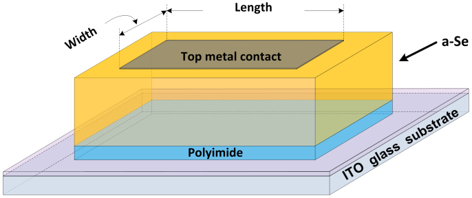
A schematic of the device structure investigated in this research, which is comprised of an a-Se sandwiched between a PI hole-blocking layer and a top contact is shown in Fig. 1. For the mobility measurement and comparison purposes, the thickness of the a-Se layer in one sample was 16.5 μm, comparable to that used in HARP technology (15 μm)11. This sample is used for optical measurements. For direct conversion X-ray measurements, another sample with 56 μm of a-Se (reasonable for absorption of 20 keV X-ray photons) was used. Figure 2a shows the dark current of the direct conversion X-ray device with 1 μm of PI and 56 μm a-Se. The amplitude of the dark current in this device is similar to the device with 1 μm of PI and 16 μm a-Se shown in reference 10, at the same electric field. This is due to the fact that the dominant component of dark current in a-Se devices is carrier injection from the biased electrodes4. Increasing the a-Se bulk thickness has negligible effect on dark current. PI prevents hole injection and the value of dark current after the transient decay at fields below 25 V/μm is approximately constant. By increasing the biasing voltage beyond 25 V/μm, the electron injection increases (as there is no electron blocking layer in the device investigated in this study) and we observe an increase in dark current.
Figure 1. Schematic of a-Se device structure with PI as hole blocking layer.
To prevent hole injection the PI layer is placed on top of the positively biased contact (ITO). The width and length of the device are both 0.6 cm.
Figure 2. Dark current of direct conversion X-ray device.
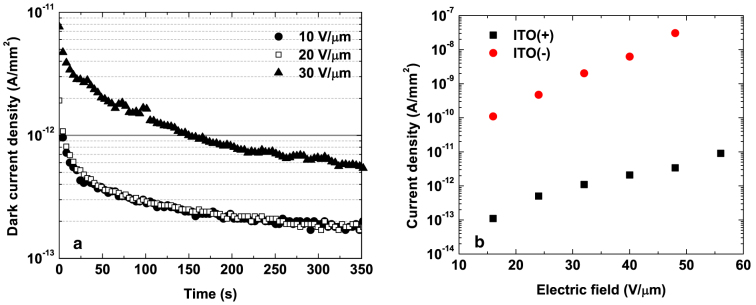
(a) Dark current density as a function of time for an ITO-PI (1 μm)-a-Se (56 μm)-Au device for different applied biased voltages. (b) Dark current density at different electric fields when the ITO is biased positively (+) and negatively (−).
In order to demonstrate that the dark current is due to hole injection and that the PI layer prevents this injection, the ITO bias is changed from positive to negative in Fig. 2b. The dark current value reported in Fig. 2b is sampled at 350 s from the initial time the bias is applied. It can be seen that the dark current remains below 10 pA/mm2 at 56 V/μm. The dark current values reported here are comparable with previously reported results from the HARP sample11. However, it should be noted that in reference 11, the HARP sample has a resistive interface layer between a-Se and the negatively biased electrode. This layer may prevent electron injection, which could explain the slightly lower dark current in the HARP sample (e.g., approximately 5 pA/mm2 at 60 V/μm for the HARP sample compared to 9 pA/mm2 at 56 V/μm for the PI sample).
TOF measurement
The time-of-flight (TOF) technique was used to investigate charge transport and collection properties in the device with the PI blocking contact. The analysis of transport properties of this device is important in determining the effect of the PI layer on transient response and verifying the nature of the gain mechanism reported in reference 10. Previously a device with a PI layer was shown to provide gain10, however it was not conclusively attributed to avalanche multiplication. It has been well documented that at high electric fields, a-Se exhibits avalanche multiplication gain12. The presence of avalanche multiplication can be verified through TOF measurements by observing an exponential increase (as opposed to a rectangular shape) in the photocurrent from a light pulse12. A schematic diagram of the TOF experimental setup is shown in Fig. 3.
Figure 3. Schematic diagram of the experimental setup for Time-of-Flight (TOF) measurements.
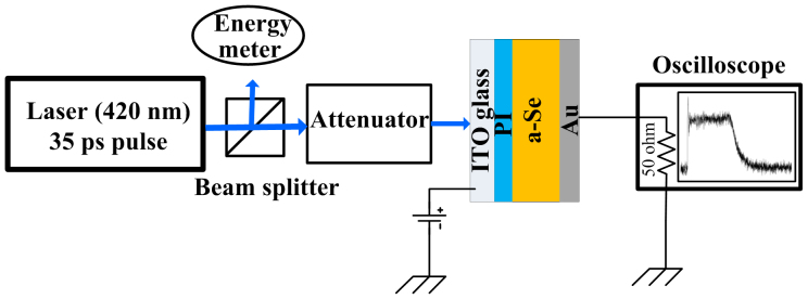
The device is exposed from the ITO side and the photocurrent transients are monitered at different electric fields by an oscilloscope. The electric field within the device is created by positively biasing the ITO layer.
For TOF measurements, short laser pulses of approximately 35 ps with a wavelength of 420 nm were used. The absorption depth of a 420 nm wavelength photon within a-Se is very short and nearly all electron-hole pairs are generated close to the PI/a-Se interface. Electrons are collected by the ITO contact and holes traverse the thickness of a-Se to get collected by the Au contact. If there is significant accumulation of electrons at the PI/a-Se interface, the electric field will drop within the a-Se layer.
Figure 4 shows TOF measurement results at electric fields below and above the field threshold required for avalanche multiplication. The signal amplitude in TOF measurements depends on the electric field in the device (because of the change in generation of electron-hole pairs) and the incident energy of laser directed to the sample, which is a function of laser energy (E) and attenuation (Attn). As the electric field changes, the current amplitude as a function of time changes. As it is seen from Fig. 4a, the hole transient response below the avalanche regime has a quasi-rectangular shape with a well-defined knee that corresponds to the hole transit time, th. The photogenerated electron's contribution to the photocurrent could be neglected due to rapid collection of the electrons by positively biased electrodes close to where electron-hole pair generation takes place. These results are very promising that there is no significant charge trapping within the device.
Figure 4. TOF signal from a-Se/PI device structure demonstrating the device is capable of reaching avalanche regime.
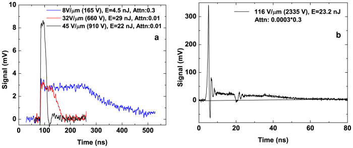
(a) Device biased at an electric field below avalanche regime. (b) Device biased at an electric field in avalanche regime. The voltage in parentheses refers to the bias voltage across the device, E refers to the energy of the laser pulse measured by the energy meter and Attn. refers to the attenuator transmission (see Fig. 3). The ringing in the measured results is from reflections caused by improper impedance matching.
The shape of the photocurrent at electric fields higher than 80 V/μm, which is the electric field threshold for initiation of avalanche multiplication for devices with approximately 16 μm thick a-Se, is different from that of fields below avalanche (Fig. 4b). The hole transient response in the avalanche regime increases rapidly due to impact ionization of holes followed by a long tail (ending around 50 ns) due to secondary non-avalanching electrons that are much slower in transport.
Hole drift mobility μh in the a-Se/PI structure is calculated by using th derived from TOF measurement results and substituting it in
 |
where d is the a-Se layer thickness and Va-Se is the voltage drop across the a-Se layer. In order to calculate the voltage drop across a-Se, the device was simulated (using MEDICI, Synopsis Inc.) and it was found that 80 percent of the applied bias voltage drops across the a-Se. This allows for an estimation of the electric field in a-Se. The simulation does not consider the field-dependent conductivity within the selenium or the effect of impurities on the electric field saturation inside selenium13.
Voltage dependence of hole drift mobility is shown in Fig. 5. Mobility increases by increasing the applied voltage and it saturates at a value of approximately 0.75 cm2/Vs. This trend is in agreement with what has been previously reported for a-Se devices14.
Figure 5. Characterization of hole mobility variation with bias voltage.
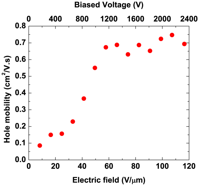
Hole mobility is determined using equation (1). The voltage value reported refers to the device bias voltage and not the voltage drop across the a-Se layer. The electric field is the field in a-Se obtained by simulations.
Lag and ghosting measurements
A requirement for any photoconductor material to be used in a direct conversion detector is to absorb a significant amount of incident X-ray photons. Selenium has a low k-edge energy of around 13 keV which makes it a well suited material for mammography with a typical mean X-ray energy of around 17 keV. For the X-ray exposure measurements, the sample with a 56 μm thick a-Se layer was used to absorb most of the incident X-rays. In order to investigate the effect of the PI layer as a hole blocking layer in direct conversion X-ray measurements, the sample behavior was studied once when ITO is positively biased such that the PI layer prevents injection of holes to the a-Se layer, and once when Au is positively biased such that there is no blocking layer to prevent hole injection. The schematic diagram of the experimental setup used in this study is shown in Fig. 6a.
Figure 6. Detector performance characterization using X-ray exposures.
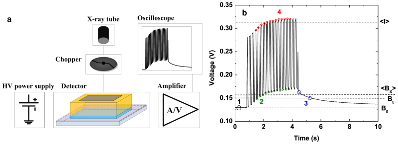
(a) Schematic diagram of the experimental setup for X-ray temporal performance. (b) A measured oscilloscope output using an X-ray pulse of 3.6 s for Au (+) biasing. Numbered regions refer to the following. 1 (B0): dark current measured before X-ray exposure; 2: dark current value measured during X-ray exposure (with chopper) used to calculate mean dark current value (<Bx>); 3 (Bt): the dark current measured at t seconds after X-ray exposure; 4: photocurrent value measured during X-ray exposure (with chopper) used to calculate mean photocurrent value (<I>).
In order to investigate the temporal performance of the detector with and without a blocking contact, we need to pulse the incident X-rays and calculate lag and ghosting using repeated X-ray exposures over time15. Lag is the increase in signal level after an X-ray exposure and ghosting is the change in X-ray sensitivity as a result of the previous exposure. The X-rays are pulsed at a frequency of 5 Hz using a rotating chopper. Each exposure was 4 s long, during which the sample was exposed to 20 X-ray pulses (100 ms with the shutter closed and 100 ms with the shutter open), resulting in approximately 1 Roentgen (R) of total exposure, where 3876 R of ionizing radiation is required to produce 1 C of ionization charge in 1 kg of air. We repeat the X-ray exposure 20 times with a time interval between subsequent exposures of approximately 80 s due to limitations of the X-ray tube. The output of one of these measurements is shown in Fig. 6b.
As can be seen from Fig. 6b, the dark current increases during the X-ray exposure. This can be due to the fact that in the presence of X-ray generated charge, there is an increased electric field at the metal/blocking layer and metal/a-Se interfaces that increases the injection from the contacts to the device. Therefore, to calculate the sensitivity (S) of the detector, which is defined as the difference between the current output of the detector during X-ray exposure (I) and the current due to increased injection (B), the average of I, (<I>) and average of B, (<Bx>) are used. This follows the convention described in reference 15. The data points used for calculating (<Bx>) and (<I>) are marked in Fig. 6b by the numbers 2 and 4, respectively. The first and last three points were not included in the calculation because the X-ray tube and chopper are not synchronized and there is fluctuation at the beginning and end of each exposure. B0 is the value of dark current before any X-ray exposure and Bt is the dark current measured at t seconds after an X-ray exposure. The lag can be quantified as either
 |
or
 |
Equation (2) is the lag as a function of time after a 4 s, 1 R exposure and equation (3) is the average lag during 5 Hz pulsed exposure of 1 R over 4 s. Depending on the value of t the lag associated with equation (3) can be smaller or larger than the value of lag calculated from equation (2). For example, the first data point marked as 3 in Fig. 6b is the dark current measured at 0.05 s after the X-ray exposure and its value is larger than <Bx> and leads to a larger reported lag compared to lag calculated from equation (3). The next shown data point is the dark current measured at 0.8 s after the X-ray exposure and its value is smaller than <Bx> and leads to a smaller reported lag value.
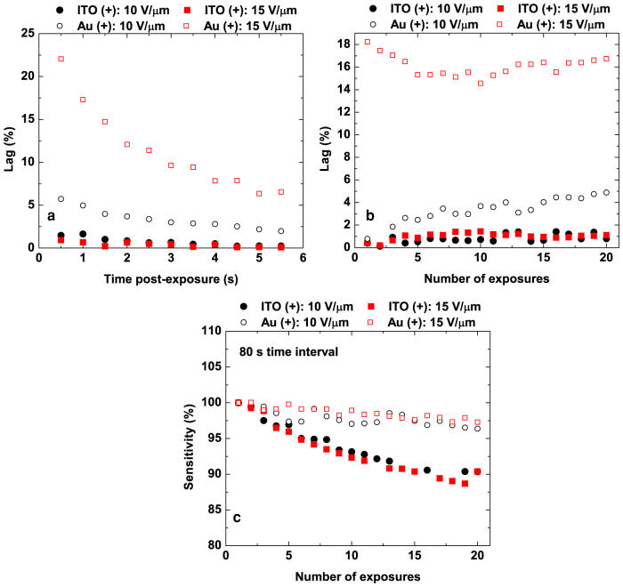
Figure 7a shows the lag as the percentage of residual signal as a function of time after the first X-ray exposure using equation (2). As can be seen in the figure, lag is decreasing with increasing time after exposure and is therefore strongly dependent on frame rate. Another conclusion from Fig. 7a is that the dominant mechanism for lag is increased carrier injection from the electrodes during exposure. When ITO glass is positively biased, PI acts as a hole blocking layer and prevents injection of holes resulting in very low dark current. As a consequence, when the voltage increases there is no increase in lag and the lag is even slightly smaller for 15 V/μm compared to 10 V/μm. On the other hand, when Au is positively biased there is no hole-blocking layer, which leads to high device dark current, and as voltage increases, the dark current increases further. Therefore, the lag becomes worse at 15 V/μm compared to 10 V/μm. Figure 7b shows the lag as a function of exposure using equation (3). As the total exposure to the device increases there is a build-up of trapped electrons throughout the a-Se layer, which increases the electric field at the positively biased contact. When the ITO is positively biased lag is essentially constant with increasing number of exposures. This is due to the PI layer preventing an increase in hole injection as the electric field increases at the ITO contact. However, when Au is positively biased at 10 V/μm, lag increases with the number of exposures. This can be explained by considering that as the density of electron traps increases with exposure, the electric field at the interface of Au and a-Se increases, leading to injection of more carriers (which is the mechanism responsible for lag). The large difference of lag between 15 V/μm and 10 V/μm can be explained by the significant increase in the dark current when increasing the bias voltage with no blocking layer. At 15 V/μm lag initially decreases as the large number of injected holes recombines with trapped electrons. The build-up of trapped electrons increases with total exposure and lag reaches a steady-state with an equilibrium between recombination and trapping.
Figure 7. Temporal performance characterization.
(a) Lag measurement results as a function of time after the first X-ray exposure for the positively biased ITO and positively biased Au at 560 V (10 V/μm) and 840 V (15 V/μm). (b) Lag measurement results using <Bx> for 20 exposures with 80 s interval time between exposures. (c) Ghosting measurement results with 80 s interval time between exposures for the positively biased ITO and positively biased Au at 10 V/μm and 15 V/μm.
Ghosting is quantified as the ratio of sensitivity measured at the n-th X-ray exposure (Sn) to the first X-ray exposure (S1)
 |
Figure 7c shows the ghosting measurements with 80 s time interval between exposures using equation (4). The drop in percentage of X-ray sensitivity is much less when Au is positively biased (less than 3 percent) compared to when ITO is positively biased (approximately 10 percent) during 20 exposures. This trend is opposite to what was observed for lag. During the X-ray exposure, electron and hole traps are created in the bulk of a-Se. This trapping reduces X-ray sensitivity. The electron trap release time is longer than the hole trap release time. In a device with high dark current, the injected hole carriers recombine with trapped electrons, in turn reducing the trapping of X-ray generated carriers.
Discussion
The effectiveness of a PI layer as a blocking layer in an a-Se device was investigated from several different aspects. TOF measurement results on the transport properties of the a-Se/PI structure confirmed that the presence of the PI layer does not create charge trapping at the a-Se/PI interface so there is no deterioration of a-Se device performance. The results also indicate that the mobility of the device increases by increasing the voltage across the device. As it is shown in Fig. 5, the increase in mobility happens at a faster rate up to a field of 60 V/μm and levels off after reaching approximately 0.7 cm2/Vs. Sufficiently low dark current (<10 pA/mm2) was also demonstrated using the PI as a hole blocking layer for electric fields up to 60 V/μm (Fig. 2b). Above 60 V/μm, there is no advantage in increasing electric fields because the hole mobility saturates. For application where impact ionization is of interest and gain is desirable, the field should be above 80 V/μm. The avalanche multiplication in a-Se/PI device was confirmed at high bias voltages through optical TOF measurements. Although for the device tested in this study the a-Se layer was 56 μm thick, typical a-Se thicknesses for commercial direct conversion X-ray detectors are in the range of 150–200 μm. In order to prevent applying very high and therefore impractical bias voltages needed for avalanche across the device (e.g., achieving 80 V/μm for a 200 μm thick device would require a bias voltage of 16,000 V), embedding grid-type electrodes within the a-Se layer16 can create a high field region near the collecting electrode which would relax bias voltages requirements due to the proximity of the embedded grid and collecting electrode.
The temporal response characteristics of the direct conversion X-ray detector a-Se/PI device structure were tested. The lag was significantly improved when using the PI layer while the ghosting appeared to degrade. When an effective hole-blocking layer is used, such as PI, a low dark current below 10 pA/mm2 critical for imaging applications can be maintained at the cost of an apparent increase in ghosting. The reason for observing less ghosting when the Au is positively biased is because the high hole injection (i.e. large component of dark current) from the Au contact leads to recombination of trapped electrons, which restores the electric field thus giving the appearance that ghosting is less. However, that has only come at a cost of high dark current leading to an unusable device for imaging. Although not observed in this research, there is a possibility for radiation damage to affect the properties of the PI layer. An investigation into the radiation hardness of the PI-layer when used as a direct conversion X-ray detector hole-blocking layer is left for future work. The device structure uses a simple, low-cost, large area compatible fabrication process and has potential usefulness in low-dose imaging applications, especially when the device is operated at high electric fields.
Methods
Device fabrication
The PI used for this investigation was the commercially available PI-2600 series from HD MicroSystems. The substrates were Corning 1737 F glass having one surface coated with 50 nm of indium tin oxide (ITO glass). All substrates were carefully cleaned using acetone followed by isopropanol in an ultrasonic bath, and were rinsed using deionized water. After drying the substrates via nitrogen flow, the PI solution was spin-coated on the ITO glass to form the PI layer. The PI samples were thermally cured at 350°C in dry air using the parameters indicated in reference 17. The PI film thickness was measured using a Dektak surface profiler and verified the expected thickness (1 μm) based on the spin coating parameters in reference 17. Stabilized a-Se alloy (containing 0.2% As and 5 ppm Cl) was thermally evaporated to create two samples of different thicknesses for the purposes of this research. Finally, a 50 nm thick layer of gold (Au) was thermally evaporated on all the samples as a top contact.
TOF measurement
The initial energy of the pulse is quite high and must be attenuated to acceptable amounts by the attenuator, which has a corresponding attenuation coefficient, Attn. The beam splitter directs 4% of the light to the energy meter (where the light energy, E, is measured). The other 96% is directed towards the attenuator. The light energy to the sample is obtained by 24*E*Atten.
X-ray exposure measurements
The dark current decreases after applying the high voltage and it is reported that it decays more than two orders of magnitude during the first 1000 s18. As a consequence, and to be consistent, we wait 20 min after applying the high voltage for the dark current to become approximately stable before exposing the sample to X-rays. The sample was exposed to optical photons and was rested for 24 h before changing the polarity of the high voltage from ITO positive to Au positive.
A Giotto IMS mammography system was used for X-ray production. The X-ray anode tube is a molybdenum (Mo) target with an additional 20 μm Mo filter. For all of the experiments, the tube potential was 32 kVP which produced a mean energy of 20 keV. The dosimeter used to measure the exposure was placed at the same position with respect to the X-ray tube as the device. A low noise current amplifier (427 model, Keithley) with programmable gain and bandwidth was used to create a voltage output that was captured on the oscilloscope. A Uniblitz (VCM-D1) shutter driver and a rotating chopper were used to pulse the X-ray exposure at a frequency of 5 Hz.
Author Contributions
S.A. and K.S.K. designed the selenium-polyimide device and experiments reported in figures 1,2,5,6 and 7; A.R. and O.B. designed the time of flight experimental research reported in figures 3 and 4; S.A., C.C.S. and O.B. performed experiments; S.A., A.R. and K.S.K. analyzed data and S.A. wrote the manuscript with suggestions from C.C.S., A.R., O.B. and K.S.K. S.A. and O.B. prepared figures 3 and 4, S.A. and C.C.S. prepared figures 6 and 7 and S.A. prepared figures 1, 2, and 5. All authors reviewed the manuscript.
Acknowledgments
This work was partly supported by the Natural Sciences and Engineering Council for Canada, Canada Foundation for Innovation, and the Ontario Research Fund. The authors express their sincere thanks to John A. Rowlands for helpful discussions on the results reported in figures 3 and 4.
References
- Que W. & Rowlands J. A. X-ray photogeneration in amorphous selenium: Geminate versus columnar recombination. Phys Rev. B. 51, 10500–10507 (1995). [DOI] [PubMed] [Google Scholar]
- Frey J. B. et al. Dark current in multilayer stabilized amorphous selenium based photoconductive x-ray detectors. J. Appl. Phys. 112, 014502-1-9 (2012). [Google Scholar]
- Wronski M. M. et al. A solid-state amorphous selenium avalanche technology for low photon flux imaging application. Med. Phys. 37, 4982–4985 (2010). [DOI] [PMC free article] [PubMed] [Google Scholar]
- Johanson R. E., Kasap S. O., Rowlands J. A. & Polischuk B. Metallic electrical contacts to stabilized amorphous selenium for use in X-ray imaging detectors. J. Non-Cryst. Solids 227–230, 1359–1362 (1998). [Google Scholar]
- Tanioka K. High-gain avalanche rushing amorphous photoconductor (HARP) detector. Nucl. Intrum. Meth. A 608, S15–S17 (2009). [Google Scholar]
- Kikuchi K. et al. Hole-blocking mechanism in high gain avalanche rushing amorphous photoconductor (HARP) film. Phys. Status Solidi (c) 8, 2800–2803 (2011). [Google Scholar]
- Nariyuki F., Imai S., Watano H., Nabeta T. & Hosoi Y. New development of large-area direct conversion detector for digital radiography using amorphous selenium with C60-doped polymer layer. Proc. SPIE 7622, 762240 (2010). [Google Scholar]
- Campbell I. H. Improving the spectral response of amorphous Se photodetectors using organic semiconductors. Appl. Phys. Lett. 4, 063303-1-3 (2011). [Google Scholar]
- Abbaszadeh S., Du Z., Allec N. & Karim K. S. Application of organic semiconductors in amorphous selenium based photodetectors for high performance X-ray imaging. Proc. SPIE 8668, 86683Q (2012). [Google Scholar]
- Abbaszadeh S., Allec N., Ghanbarzadeh S., Shafique U. & Karim K. S. Investigation of hole-blocking contacts for high-conversion-gain amorphous selenium detectors for x-ray imaging. IEEE Trans. Electron Devices 59, 2403–2409 (2012). [Google Scholar]
- Bubon O., DeCrescenzo G., Rowlands J. A. & Reznik A. Amorphous selenium (a-Se) avalanche photosensor with metal electrodes. J. Non-Cryst. Solids 358, 2431–2433 (2012). [Google Scholar]
- Juska G. & Arlauskas K. Feature of hot carriers in a-Se. Phys. Status Solidi (a) 77, 387–391 (1983). [Google Scholar]
- Juska G. & Arlauskas K. Impact ionization and mobilities of charge carriers at high electric fields in amorphous selenium. Phys. Status Solidi (a) 59, 389–393 (1980). [Google Scholar]
- Bubon O. et al. Electrode avalanche amorphous selenium (a-Se) photosensor. Curr. Appl. Phys. 12, 983–988 (2012). [DOI] [PMC free article] [PubMed] [Google Scholar]
- Zhao B. & Zhao W. Temporal performance of amorphous selenium mammography detectors. Med. Phys. 32, 128–136 (2010). [DOI] [PubMed] [Google Scholar]
- Goldan A. H. & Zhao W. A field-shaping multi-well avalanche detector for direct conversion amorphous selenium. Med. Phys. 40, 010702 (2013). [DOI] [PMC free article] [PubMed] [Google Scholar]
- MicroSystems H. D. PI-2600 Series – Low Stress Applications, Product Bulletin, http://hdmicrosystems.com/HDMicroSystems/en_US/pdf/PI-2600_ProcessGuide.pdf, November 28, 2010. [Google Scholar]
- Kasap S. O. & Belev G. Progress in the science and technology of direct conversion X-ray image detectors: The development of a double layer a-Se based detector. J. Optoelectron Adv. M. 9, 1–10 (2007). [Google Scholar]


