Abstract
We present a novel method to fabricate flexible and tunable plasmonic nanostructures based on combination of soft lithography and nanosphere lithography, and perform a comprehensive structural and optical characterization of these structures. Spherical latex particles are uniformly deposited on glass slides and used as molds for polydimethylsiloxane to obtain nanovoid structures. The diameter and depth of the nanostructures are controlled by the size of the latex particles. These surfaces are coated with a thin Ag layer for fabrication of uniform plasmonic nanostructures. Structural characterization of these surfaces is performed by SEM and AFM. Optical properties of these plasmonic nanostructures are evaluated via UV/Vis absorption spectroscopy, dark field microscopy, and surface–enhanced Raman spectroscopy (SERS). Position of the surface plasmon absorption depends on the diameter and depth of the nanostructures. SERS enhancement factor (measured up to 1.4 × 10⁶) is dependent on the plasmon absorption wavelength and laser wavelength used in these experiments.
Surface plasmons (SPs) are collective excitation of free conductive electrons on noble metal thin films or nanoparticle surfaces excited by electromagnetic radiation at the metal-dielectric interface1. The study of the interaction between light and metallic nanostructures is a rapidly emerging research area known as plasmonics, which is the branch of the nanophotonics field2,3,4,5. Plasmonic nanostructures have the ability to control and manipulate visible light at the nanometer scale6,7,8. Examples of plasmonic devices include plasmonic filters6, wave-guides6,7,8, and nanoscopic light sources9. In addition, the research area dealing with the interaction of molecules or molecular structures with plasmonic nanostructures is another rapidly growing field, due to potential analytical applications such as surface-enhanced Raman spectroscopy (SERS)10, localized surface plasmon resonance (LSPR) spectroscopy11, and surface plasmon resonance (SPR) spectroscopy12,13. Plasmonic nanostructures have also been used in biomedical applications, due to their tunable response (absorption and scattering) to incident light14. Several studies involving the use of plasmonic nanostructures in biophysical research15,16, biomedical imaging and sensing17,18 and medical diagnostic19 and cancer therapy20,21 have been reported in the literature.
There are two types of surface plasmons: (i) propagating and (ii) non-propagating1,22. Propagating surface plasmons are called surface plasmonpolaritons (SPRs) generated on noble (such as Au or Ag) metallic thin films (10–200 nm in thickness). Non-propagating surface plasmons, on the other hand, are called localized surface plasmon resonances (LSPRs) and are generated on the surface of nanoparticles of 10–200 nm in size22,23. For SPRs, the electromagnetic field generated on the noble metallic thin film propagates in the x- and y- directions in the range of 10–100 μm and in z- direction in the range of 200–300 nm along the metal-dielectric interface, depending on the type of metal, film thicknesses, and surface roughness of thin film5,23,24. However the electromagnetic field of the LSPRs decays exponentially away from the surface of the nanoparticle, extending to only a few nanometers25. The plasmonic properties of metallic nanoparticles are strongly dependent on their type, size, shape, and composition, as well as the dielectric environment26,27,28,29.
The synthesis and preparation of plasmonic nanostructures is a research area with a significant impact on various applications to photonics, opto-electronics3,4, electronics30,31, chemical and biological sensing23,32,33, medical diagnostics and therapy20,21. Two approaches are commonly used for the preparation of plasmonic nanostructures: bottom-up and top-down34. The bottom-up approach involves the reduction of metal salts or assembly of nanoparticles in suspension or on the surface35,36,37. On the other hand, the top-down approach is based on the preparation of the structure on smooth thin films using lithographic techniques38,39,40 such as electron beam lithography (EBL)41,42 and focused ion beam (FIB)43,44,45 lithography. The advantage of these techniques is the precise size control of the nanostructure, but is associated with high cost, small area of the structure, and long manufacturing time46. Alternative methods such as nanosphere lithography47 and soft lithography48 are also used for the preparation of plasmonic structures.
Preparation of tunable plasmonic nanostructures is essential for SERS applications. Higher SERS enhancement factors are obtained when the wavelength of the LSPR of the nanostructure (λLSPR) is located between the excitation wavelength (λexc) and the wavelength of Raman signal (λRS)49. Theoretical and experimental results demonstrated that the maximum enhancement occurs when the λLSPR is equal to the average of the λexc and the λRS; that is, λLSPR = ½(λexc + λRS)50,51,52,53. Various advanced methods have been employed to fabricate 3D well-defined nanostructures to control and manipulate the plasmonic properties in order to maximize the enhancement factor for SERS experiments54,55,56,57,58,59,60,61,62,63,64,65. Nanoholes and nanovoids have been used as SERS substrates. Nanoholes were prepared using EBL56,60, FIB57 or soft lithography55,58,64, while the nanovoid arrays were prepared using porous anodic alumina65 or the combination of nanosphere lithography and electrochemical deposition technique54,61,62. In these methods, plasmonic properties were tuned by changing the diameter and periodicity (hole spacing) of the nanoholes to obtain the maximum SERS enhancement56,57,60. For nanovoids, changing the void diameter and height was used to tune their plasmonic properties54,61. The reported enhancement factors obtained from nanoholes and nonovoids are around 104–106 55,56,57,58,60.
In this study, we used a simple method consisting of a combination of soft lithography and nanosphere lithography to fabricate large area, tunable, and mechanically flexible plasmonic nanostructures. Soft lithographic methods that use elastomers such as polydimethylsiloxane (PDMS) offer three important advantages: parallelism, simplicity, and flexibility. Nanosphere lithography, on the other hand, uses small spherical particles to obtain a template for lithography. In our study, spherical sulfate latex particles with different diameters were deposited on a regular glass slide and used as template for the PDMS elastomer. PDMS elastomer was poured on the deposited latex particles and cured to obtain bowl-shaped nanovoids on the PDMS surfaces. The Ag layer (60 nm) was sputtered on the PDMS with and without Cr (5 nm) to obtain flexible plasmonic nanostructures. The plasmonic properties of these nanostructures were tuned by changing the size of the latex particles. For larger particles, larger diameter and deeper nanovoids were obtained. For smaller particles, smaller diameter and shallower nanovoids were obtained. The structural properties were characterized using scanning electron microscopy (SEM) and atomic force microscopy (AFM). The characterizations of optical properties of nanostructure were performed using UV/Vis absorption spectroscopy, dark field microscopy, and SERS.
Similar substrates have been previously reported in the literature54,65. These SERS-active nanovoids substrates were prepared by assembling a monolayer of uniform polystyrene colloidal particles onto a gold coated surface and then electrodepositing gold through this template to produce rigid nanovoids with controlled thicknesses. The nanovoids prepared in this way are not flexible and need a pre-prepared gold-coated surface. In addition, the colloidal particles must form monolayer to grow gold and generate nanovoids. In these studies, the plasmonic modes were tuned by changing the diameter of colloidal particles and thickness of the deposited gold54,65. In contrast, our substrate is flexible and we are using only the top layer of the deposited colloidal particles. Therefore, this method does not need a monolayer of colloidal particles, simplifying the fabrication procedure.
Flexible substrates have also been prepared66. However, our substrate is prepared in a simpler way without the electrochemical deposition step described in66 and we show and characterize substrates with different nanovoid sizes. We also demonstrate the utility of such substrates for SERS measurements.
Results
Preparation and structural characterization of flexible nanostructures
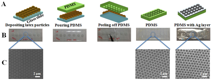
The combination of nanosphere lithography and soft lithography was used to fabricate tunable and flexible plasmonic nanostructures. Figure 1 A–C shows the schematic, photographs, and SEM images illustrating the fabrication steps of plasmonic nanostructures. First, colloidal latex particles (1600 nm, 1400 nm, 1200 nm, 1000 nm, 800 nm, and 600 nm in diameter) were assembled from a droplet on a regular glass slide. The dropped latex particles were quickly dried in the oven to eliminate preferential accumulation of particles on the outside of the droplet (a phenomenon known as the coffee ring effect), and obtain a uniform assembly of particles on the surface. More than one layer of particles can be obtained in this way, which is not critical for this approach. Next, viscous PDMS elastomer was poured onto the deposited latex particles and cured in an oven for 2 hours at 100°C. The PDMS filled all the voids and covered the latex particles. The PDMS was then peeled off from the surface. Depending on size of the latex particles, bowl–shaped nanovoids with different diameters and depths were obtained at the bottom surface of PDMS. The peeled PDMS was washed to remove the latex residues and was then used as mold for the fabrication of nanovoid plasmonic structures by Ag (60 nm thickness) or Cr (5 nm) + Ag (60 nm) layer sputtering. Cr was used as adhesion layer between PDMS and Ag.
Figure 1. Schematic (A), photographs (B), and SEM images (C) of the preparation steps of bowl-shaped nanovoidplasmonic nanostructures.
SEM characterization of the structures
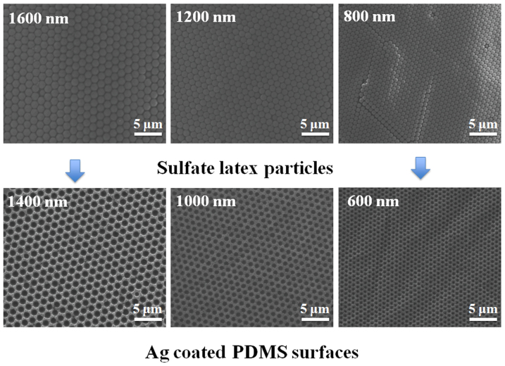
SEM was used to characterize the self-assembly of latex particles and plasmonic nanostructures on PDMS surfaces. Figure 2 shows the SEM images of latex particles with three different sizes (1600 nm, 1400 nm, and 800 nm) assembled on the glass slide and plasmonic nanovoids obtained on the PDMS surface using these latex particles. The assembled latex particles are very uniform and closely packed on the glass slide, as seen in the Figure 2. The diameter of metal-coated voids produced on the PDMS surface was approximately 200 nm smaller then the size of the latex particles, due to the thickness of the added metal layer. For example, when the 1200 nm latex particles were used as mold for the PDMS, the diameter of coated PDMS was around 1000 nm. As shown in Figure 2, bowl-shaped nanovoids with different diameters and depths can easily be prepared by using different sizes of latex particles.
Figure 2. SEM images of the assembled latex particles (1600 nm, 1200 nm, and 800 nm in diameter) on the glass slides and Ag coated PDMS surface prepared using the corresponding size of latex particles.
Please note that, due to the metallic layer, the size of nanovoids is smaller than the size of the latex particles.
AFM characterization
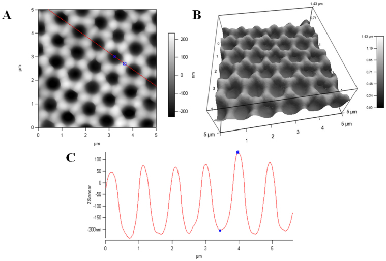
Next we used AFM to determine the depth of the nanovoids on the PDMS surfaces. Figure 3 shows representative AFM 2D and 3D images (5 μm x 5 μm), as well as a line profile (depth scan) of the coated PDMS surfaces prepared using 1000 nm latex particles.
Figure 3. AFM images of Ag coated PDMS prepared with 1000 nm latex particles (A), 3D image of the A (B), and line scan obtained across the red line shown in A (C).
The size of voids was measured to be around 800 nm, which is also consistent with SEM images (200 nm smaller). The nanovoids can easily be seen on 3D AFM image (Figure 3B). The line analysis was performed to demonstrate the uniformity and measure the depths of the voids. The depth of Ag coated PDMS was around 300 nm when the 1000 nm latex particles were used, and it appears to be very uniform across many voids (Figure 3 C). The summary results of structural characterization can be found on the Table 1.
Table 1. Structural characterization results obtained from SEM and AFM images.
 |
||||||
| Diameter of Latex Particles (nm) | 1600 | 1400 | 1200 | 1000 | 800 | 600 |
| Diameter of Ag Coated PDMS (nm) | 1400 | 1200 | 1000 | 800 | 600 | 400 |
| Depth of Ag Coated PDMS (nm) | 600 | 500 | 400 | 300 | 200 | 100 |
Optical characterization of plasmonic nanostructures
We used several techniques for optical characterization of plasmonic nanostructures: UV/Vis absorption spectroscopy, dark field microscopy, and SERS.
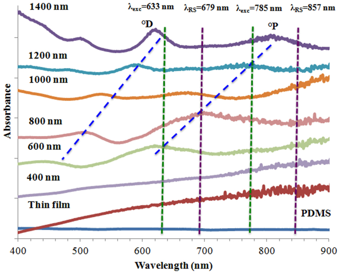
UV/Vis absorption spectroscopy is routinely used for the characterization of plasmonic structures. The absorption spectra helped us determine the spectral position of the plasmon resonance. The PDMS plasmonic surface area was cut with a scalpel and placed inside a disposable plastic cuvette to perform a wavelength scan (400–900 nm). Figure 4 shows the absorption spectra of prepared nanovoids on PDMS surface having six different diameters and depths, as well as a smooth thin film on PDMS and non-coated PDMS surface. The non-coated PDMS is transparent, and therefore no absorption band was observed. However, when the nanovoids were coated with a Ag layer, two main absorption bands were observed. The two dominant absorption maxima (two plasmonic modes) were obtained for all nanostructure sizes, except for the 400 nm voids and Ag thin film on PDMS, which appear to have a similar appearance.
Figure 4. UV/Vis absorption spectra obtained from plasmonic nanovoid structures having different sizes, smooth thin film of Ag on PDMS and uncoated PDMS.
The shift in the position of the absorption bands is indicated with blue lines, and the wavelengths of excitation and Raman signal are marked as vertical lines with green and purple, respectively.
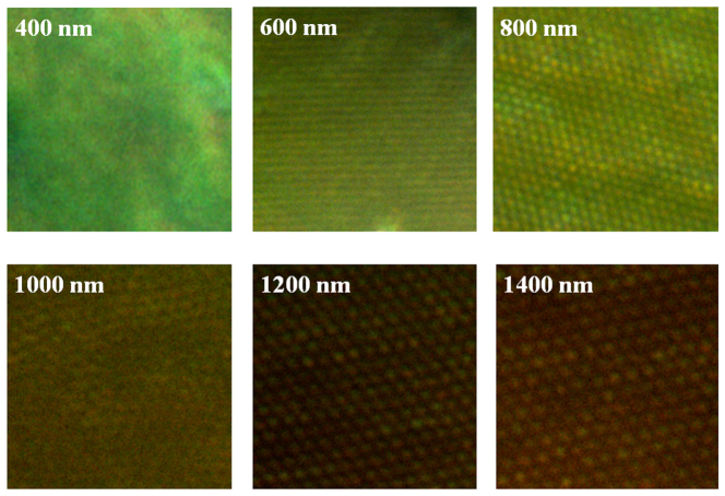
Dark field microscopy was also used for the optical characterization of the plasmonic nanostructures. The color obtained from the dark field microscope is correlated to the scattering of the light by the nanostructures. The dark field images of the plasmonic structures with different void sizes are presented in Figure 5. The voids having larger sizes appear red under the dark field microscope. However, when the void size decreases, the color of the surfaces transitions from brown to yellow, then green, suggesting that the scattering wavelength of the plasmonic structures shifts to shorter wavelengths. This is consistent with the results obtained from the absorption spectra of the nanostructures.
Figure 5. Dark-field microscopy images of plasmonic nanostructures with different sizes (from 400 nm to 1400 nm).
SERS measurements
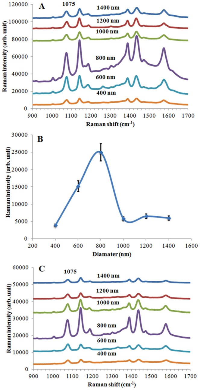
Finally, the optical characterization of fabricated nanostructures was performed using SERS. It is well known that the SERS enhancement is strongly dependent on the plasmonic properties of the nanostructures. Tunability of the structures allows maximization of the SERS enhancement, which is critical for analytical purposes where detection of low concentrations of analytes of interest is desired. It is well documented that the maximum enhancement is achieved when λLSPR of the nanostructures is between λexc (laser) and λRS of analyte49,50,51,52,53. Two different laser wavelengths (633 nm and 785 nm) were used to excite the analyte on the nanostructures. The SERS signal from self-assembled 4-ATP molecules was measured and used to evaluate the SERS performance of the Ag coated, flexible, bowl-shaped nanovoid plasmonic structures with different sizes and depths. Figure 6 shows the SERS spectra obtained from 4-Aminothiophenol (4-ATP) molecules (A) and peak intensity changes at 1075 cm−1 for different void sizes (B). The SERS intensity of the spectra is completely different depending on the size of the nanovoids which is related to λexc, λRS and λLSPR (marked as vertical lines in Figure 4). The peak at around 1075 cm−1 was used to evaluate the SERS performance of the structures. λRS was calculated and found to be 679 nm when the λexc is 633 nm. The maximum enhancement should be obtained when the λLSPR is approximately 656 nm, which is close to the λLSPR of plasmonic structures having 800 nm void sizes. Thus, when the nanovoid structures (800 nm) are used, maximum SERS enhancement should be obtained. The experimental results confirmed this, as maximum SERS intensity was observed for 800 nm nanovoid structure. In order to promote the adhesion of the Ag layer on PDMS, we explored the use of an additional Cr layer underneath Ag. This layer is approximately 5 nm thick and prevents the delamination of Ag during vigorous washing steps such as acid treatment. SERS spectra were obtained from 4-ATP molecules assembled on the PDMS surface coated with a Cr (5 nm) and Ag (60 nm) layer (see Figure 6C). The same trend for SERS intensity versus void size was obtained compared to Ag coated PDMS surfaces. The maximum intensity for the 1075 cm−1 peak was observed when the void size of the structure is 800 nm.
Figure 6. SERS spectra obtained from assembled 4-ATP molecules on plasmonic nanovoid structures (coated with a 60 nm Ag layer) having different sizes and depths (A) and SERS intensity changes of the 1075 cm−1 peak depending on the diameter of the nanovoids (B), and SERS spectra obtained from self-assembled 4-ATP molecules on plasmonic nanovoid structures (coated with a 5 nm Cr and a 60 nm Ag layer) having different sizes (C).
The excitation wavelength is 633 nm.
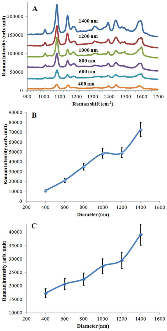
SERS spectra are also obtained using a 785 nm laser from all nanostructures coated with Ag, or Cr and Ag. The maximum enhancement conditions are different due to the use of a different λexc. λRS is 857 nm (for the 1075 cm−1peak) when the λexc is 785 nm. The maximum enhancement should be obtained when the plasmonic structures have a λLSPR at around 821 nm. When the absorption spectra of nanostructures are examined, the maximum enhancement can be obtained using nanovoids of approximately 1400 nm in size. Figure 7 shows the SERS spectra obtained from 4-ATP molecules assembled on the plasmonic nanostructures (Cr and Ag coated) having different sizes and depths (A) and peak intensity changes at 1075 cm−1depending on the size differences (B), and SERS spectra of 4-ATP assembled on the plasmonic structures (Ag coated) (C). The experimental results demonstrate that the maximum intensity was observed when the nanostructures have a diameter of 1400 nm. When the size of the nanostructures was reduced, the SERS intensity decreased (see Figure 7 B). Similar experimental results were obtained when only Ag was used to coat the PDMS surfaces (see Figure 7C).
Figure 7. SERS spectra obtained from assembled 4-ATP molecules on plasmonic nanovoid structures coated with Cr (5 nm) and Ag (60 nm) layer having different sizes and depths (A) and SERS intensity changes for the 1075 cm−1 peak depending on the diameters of nanovoids (B), and SERS intensity changes at 1075 cm−1 depending on the diameters of nanovoids coated with a Ag layer (60 nm) (C).
The excitation wavelength is 785 nm.
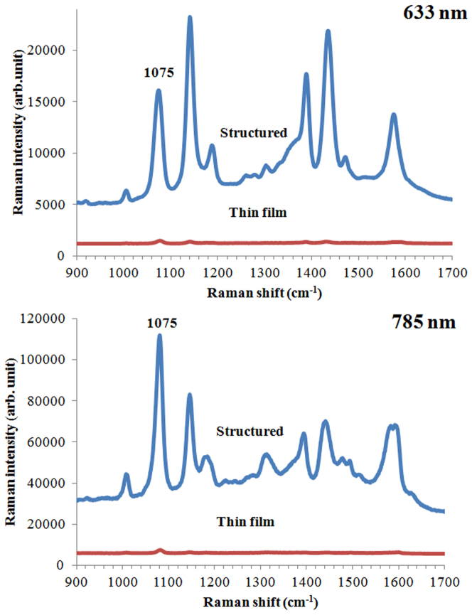
Next, SERS spectra were obtained from Cr and Ag coated thin film PDMS surfaces and compared with SERS of structured PDMS surfaces. Figure 8 shows the SERS spectra of 4-ATP molecules assembled on these surfaces. The improvement in SERS spectra obtained with smooth thin film versus structured (nanovoids) surfaces was calculated based on the peak height measured at 1075 cm−1. The SERS intensity of 4-ATP molecules on the structured surface (void diameter of 800 nm) was approximately 25 times higher than the intensity on the thin film when the 633 nm laser was used. On the other hand, a 46 times higher SERS intensity was measured for 1400 nm nanovoids when the 785 nm laser was used. A small increase in SERS intensity is expected due to larger area of the nanovoid structures, which provides a larger biding surface for the 4-ATP molecules. However, the surface area of nanovoids is only approximately 2 times higher than the area of the thin film, accounting for only a factor of two increase in intensity. When the SERS intensities obtained at the two different excitation wavelengths are compared, lower improvement is observed for 633 nm excitation. These results demonstrate that the well-defined nanovoid structures can increase electromagnetic field confinement in the voids, and can thus contribute to the enhancement of the Raman signal.
Figure 8. Comparison of SERS spectra obtained from 4-ATP assembled on plasmonic nanostructured area and smooth thin film of Ag on PDMS using 633 nm and 785 nm lasers.
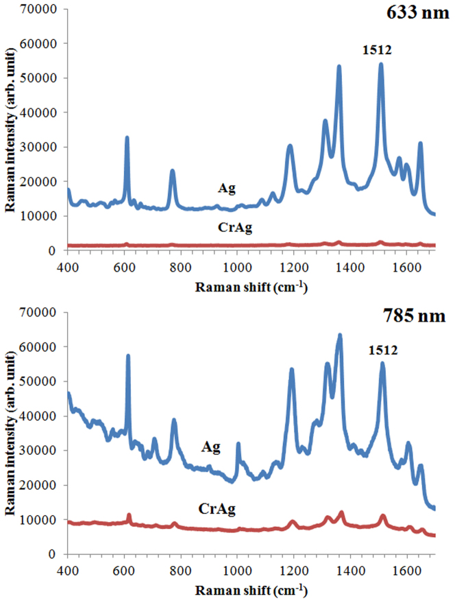
A recent report demonstrates that adhesion layers can decrease the SERS enhancement due to the deterioration of surface plasmons depending on the type and thickness of the adhesion layers using a 633 nm laser70. The SERS spectra were obtained from the Ag (60 nm) coated structures and Cr (5 nm) and Ag (60 nm) coated PDMS surfaces having 800 nm void size for 633 nm laser excitation and 1400 nm void size for 785 nm excitation wavelength to evaluate the deterioration of surface plasmons in the proposed structures using 1.0 × 10⁻⁶ M Rhodamine 6G molecules (see Figure 9). When the SERS spectra are examined, it is found that the dampening of the enhancement is larger when the 633 nm laser is used compared with an experiment where a 785 nm laser generates excitation of the Raman signal. The dampening in the enhancement is around 45 times on the Cr coated surface for 633 nm laser excitation and only approximately 10 times on the Cr coated surface when the 785 nm laser is used. The same experimental results were obtained for all sizes of structures. We found that the dampening of the surface plasmons is dependent not only on the thickness of the adhesion layers, but also on the excitation wavelength, a fact that was not previously reported. This allows us to conclude that if an adhesion layer is necessary, longer wavelengths will be more suitable for the SERS experiments.
Figure 9. SERS spectra obtained from Rhodamine 6G dropped onto structured areas coated with only Ag (60 nm), or Cr (5 nm) and Ag (60 nm) layers using 633 nm (800 nm void size) and 785 nm (1400 nm void size) lasers.
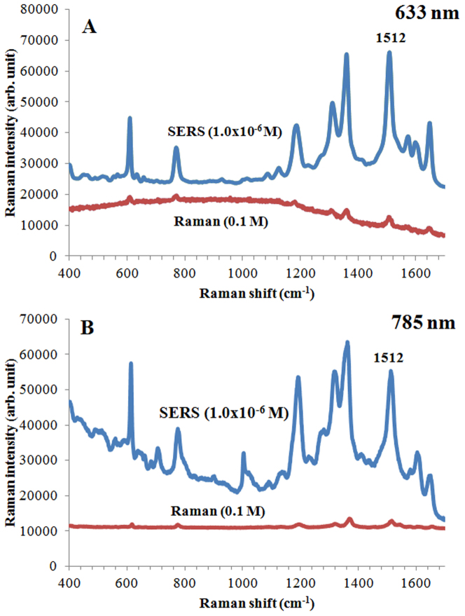
Finally, the SERS enhancement factor was calculated using Rhodamine 6G. The peak at 1512 cm−1 was used to calculate the enhancement factor for the fabricated nanostructures. Rhodamine 6G solutions at concentrations of 1.0 × 10⁻¹ M and 1.0 × 10⁻⁶ M are used for the bulk Raman and SERS experiments, respectively, using laser at 633 and 785 nm. The enhancement factor was estimated by using the formula ISERS/IBulkxCBulk/CSERS. Figure 10 shows the spectra of bulk Raman and SERS spectra of Rhodamine 6G dropped on a CaF2 slide and on nanovoid structures. Based on previous results (Figure 5 and 6) that demonstrate the maximum SERS intensity for different size PDMS structures at different excitation wavelengths, we choose 800 nm void structures for 633 nm excitation (Figure 10A) and 1400 nm void structures for the 785 nm laser (Figure 10B). The concentration factor (the ratio of the Rhodamine 6G concentration used for spontaneous Raman vs SERS) was 1.0 × 10⁵, and the intensity ratios were 14.2 and 13.1 for 633 and 785 nm lasers, respectively. From here, maximum enhancement factors of 1.42 × 10⁶ (for 800 nm nanovoids and 633 nm excitation) and 1.31 × 10⁶ (for 1400 nm nanovoids and 785 nm excitation) were determined.
Figure 10. Raman and SERS spectra of Rhodamine 6G (0.1 M and 1.0 × 10⁻⁶) dropped on a CaF2 slide and on plasmonic nanovoid structures.
Discussion
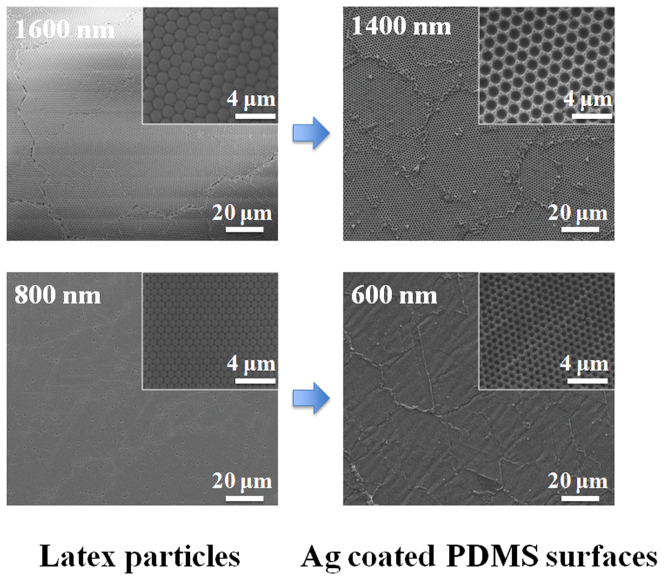
In this study we demonstrated a simple and novel method to fabricate tunable and flexible plasmonic nanostructures based on the combination of nanosphere lithography and soft lithography. We also presented a systematic and comprehensive characterization (structural and optical) of the structures. Structural characterization was performed using SEM and AFM, demonstrating that the diameters of the plasmonic nanostructures were approximately 200 nm smaller than the latex particles used as mold for the structures, due to the thickness of the metallic layer. Furthermore, the size of the structures was tunable both in depth and diameter and followed the size of the latex particles. The total area of nanostructures obtained from a single drop, while maintaining a uniform structure, is around 5 mm in diameter, which is significantly larger than the area that can be obtained with other lithography techniques. Lower magnification SEM images that demonstrate the uniformity of the structures in a larger area are shown in Figure 11 for surfaces prepared using 1600 nm and 800 nm latex particles. This demonstrates the potential for scaling up the technology. The latex particle can also be deposited on larger areas using other assembly techniques, such as convective assembly. Another important observation is that in our study the void size changes in both diameter and depth when different particle sizes are used. This is not the case in previous studies, where different particle sizes produce only changes in the diameter of the voids. The advantages of this approach are the simplicity of the method, uniformity, larger area, and flexibility of the structures.
Figure 11. SEM images of large area assembled latex particles (1600 nm and 800 nm) on the glass slides and Ag coated PDMS surface prepared using that size of latex particles.
Insets show the structures at higher magnification.
Plasmonic properties of these structures were characterized using UV/Vis absorption spectroscopy, dark field microscopy, and SERS. We observed two dominant surface plasmon absorption bands of the plasmonic structures that originated from near to bottom (°D mode) and near to center (°P mode) of the structures. Both surface plasmon modes shifted towards shorter wavelengths when the diameter of the structures was decreased. An interesting observation is that the absorbance corresponding to the °P and °D modes depends on both the size and depth of the plasmonic structures. The °D mode is more dominant at larger size and deeper structures. However, when the size and depth are reduced, the °P mode becomes more dominant. The plasmonic properties of nanovoid structures were extensively studied in the literature67,68,69. These reports suggest that the band at the shorter wavelengths is due to the surface plasmons confined near the bottom of the void, and is called °D mode. The absorption band appearing at longer wavelengths in the absorption spectra is due to surface plasmons generated near to the center of the void, and is called °P mode. The absorption of the °P mode is always at longer wavelengths compared with the °D mode68. The spectral position of these two modes is strongly dependent on the size of voids and correlates linearly with the void size. When the size of void is decreased, the absorption wavelength shifts to shorter wavelengths for both modes68. The spectra we show in Figure 4 exhibit a similar behavior (marked as blue lines), with the exception of very small voids, where the spectrum resembles the absorption profile of a thin, which is consistent with other data reported in the literature54,61,67,68.
We also obtained dark field microscopy images that confirmed the UV/Vis absorption measurements. The largest and smallest sizes of plasmonic nanostructures appeared as red and green, respectively.
Finally, SERS spectra were obtained to evaluate the plasmonic properties of the structures using Raman reporter molecules. The experimental results showed that the maximum SERS intensity was obtained when the size of nanostructures was 800 nm for 633 nm excitation and 1400 nm for 785 nm excitation. In addition, the SERS performance of nanovoid plasmonic structures was compared with that of Ag coated thin films on PDMS surfaces. At least 25 times improvement in the SERS signal was observed on the nanovoid structured surfaces vs smooth thin film. Overall, the maximum intensity (SERS enhancement) was obtained using nanovoids with 1400 nm size for 785 nm laser excitation, and 800 nm size for 633 nm laser excitation. It should be noted that, since °P mode produces the strongest electric field distribution near the center of the voids68, the SERS enhancement factor should be more dependent on the wavelength of °P mode. Indeed, the maximum SERS enhancement was obtained when the °P mode absorption wavelength is close to the calculated λLSPR.
A comparison of SERS activity of Ag coated nanovoids and Cr (adhesion layer) and Ag coated nanovoids was also performed. We noted that the expected dampening effect of the adhesion layer was dependent on the excitation wavelength, with lower dampening at longer excitation wavelengths. Finally, the SERS enhancement factor was calculated for the structures giving highest SERS intensity, using Rhodamine 6G as probe molecule. Maximum enhancement factors (1.31 × 10⁶ and 1.42 × 10⁶) were obtained for nanostructures coated with a Ag layer having 1400 nm diameter (for 785 nm laser excitation) and 800 nm diameter (for 633 nm laser excitation).
In conclusion, these nanostructures are simple to fabricate and their plasmonic properties can easily be tuned by changing the size of the latex particles used as mold. In addition, physical forces such as stretching, bending and twisting of the flexible PDMS structure can further tune their plasmonic properties. These properties combined with the high SERS enhancement factors offer great promise for their use in SERS-based sensing and characterization of biological and chemical structures. Due to the large surface area of these structures (comparable to smooth thin films), their plasmonic tunability and mechanical flexibility, they can also be used in other plasmonic-based applications such as photovoltaic devices and catalytic processes.
Methods
Chemicals
Dichloromethane, 4-ATP, ethanol, and Rhodamine 6G were purchased from Sigma-Aldrich (USA). PDMS elastomer kit was purchased from Dow Corning (USA). Sulfate latex particles (8% w/v) were purchased from Invitrogen (USA).
Fabrication of plasmonic nanostructures
A 10 μL of spherical sulfate latex particles (8% w/v) with diameters of 1600 nm, 1400 nm, 1200 nm, 1000 nm, 800 nm, 600 nm were dropped onto the cleaned regular glass slide and desiccated in the oven (at 100°C) for approximately 3 minutes to quickly dry and eliminate the coffee ring effect. The viscous PDMS elastomer was poured on the assembled latex particles and cured for 2 hours in the oven at 100°C. The cured PDMS was peeled off and washed with dichloromethane to remove the latex residues on the surface. The bowl-shaped nanovoid structures that were obtained on the PDMS surfaces were coated with 60 nm Ag layer or 5 nm Cr and 60 nm Ag layer using a sputtering instrument (Kurt J. Lesker Company).
Structural characterization
SEM and AFM were used for the structural characterization of the latex particle coatings, PDMS surfaces, and plasmonic nanostructures. All SEM images were obtained using a FEI NanoSEM instrument with an accelerating voltage of 10 kV. All AFM images were taken with an Asylum Research MFP-3D AFM (Oxford Instrument).
Optical measurements
UV/Vis absorption spectra of the plasmonic nanostructures were recorded by a Varian Cary 50 Bio UV/Visible spectrophotometer. Dark field microscopy images were performed at 100× optical magnification using a CytoViva dark field condenser coupled to an upright Olympus microscope. SERS measurements were performed with a Renishaw InVia Raman microscope with excitation wavelengths at 633 nm and 785 nm. 4-ATP and Rhodamine 6G were used as SERS probe molecules to evaluate the SERS performance of the structures. The plasmonic nanostructures (Ag coated or Cr and Ag coated) were incubated in an ethanolic solution of 4-ATP (1 mM) for 2 h to form a self-assembly monolayer (SAM) of molecules on the surface. Then, the surfaces were washed with ethanol to remove the unbound molecules from the surfaces. When the 633 nm laser is used for Ag coated nanostructures, the exposure time and laser power were 10 s and 80 μW. However, when the surfaces were coated with a adhesion layer (Cr) and a Ag layer, the exposure time and laser power were 10 s and 800 μW. When the 785 nm laser is used, the exposure time and laser power were 10 s and 100 μW for Ag coated nanostructures. However, when the surfaces were coated with an adhesion layer (Cr) and a Ag layer, the exposure time and laser power were 10 s and 1000 μW. A 10 μL of rhodamine 6G (1.0 × 10⁻⁶) was dropped on the Ag coated and Cr/Ag coated surfaces to evaluate the dampening properties of the structures. The exposure time and laser power were 10 s and 800 μW for the 633 nm laser and the exposure time and laser power were 10 s and 1000 μW for the 785 nm laser. Finally, a 10 μL of rhodamine 6G (1.0 × 10⁻¹ M) was dropped on the CaF2 slide to obtain Raman spectra, and 1.0 × 10⁻⁶ M of rhodamine 6G was dropped on the nanostructured area to obtain a SERS spectra to estimate the enhancement factor of the plasmonic structures. The exposure time and laser power were 10 s and 800 μW for 633 nm laser, and 10 s and 1000 μW for 785 nm laser. In this study, all presented SERS spectra of 4-ATP and Rhodamine 6G are the average of ten spectra obtained from arbitrarily chosen areas under the microscope for each sample. The percent coefficient of variation (CV%) of the SERS spectra was in the range of 7–12% for all structures and both lasers.
Author Contributions
M.K. and S.W.H. designed the study, interpreted the data, and wrote the manuscript. M.K. performed the experiments and analyzed the data. P.D., O.K. and E.S. performed the thin film deposition and helped writing the manuscript.
Acknowledgments
This work was supported by Agilent Technologies and NSF through NSF grant #1068109, University of California Laboratory Fees Research Program Award 12-LR-237197, University of California Davis Research Investments in the Sciences & Engineering (RISE) Award, and by the Center for Biophotonics Science and Technology, a designated NSF Science and Technology Center managed by the University of California Davis, under Cooperative Agreement no. PHY0120999. We thank Ms. An Nguyen for the help with the drawings and Dr. Ian McAlexander of Agilent Technologies for insightful comments.
References
- Stewart M. E. et al. Nanostructured Plasmonic Sensors. Chem. Rev. 108, 494–521 (2008). [DOI] [PubMed] [Google Scholar]
- Atwater H. A. The Promise of Plasmonics. Scientific American 296, 56–63 (2007). [PubMed] [Google Scholar]
- Ozbay E. Plasmonics: Merging Photonics and Electronics at Nanoscale Dimensions. Science 311, 189–193 (2006). [DOI] [PubMed] [Google Scholar]
- Maier S. A. & Atwater H. A. Plasmonics: Localization and Guiding of Electromagnetic Energy in Metal/Dielectric Structures. J. Appl. Phys. 98, 011101 (2005). [Google Scholar]
- Van Duyne R. P. Molecular Plasmonics. Science 306, 985–986 (2004). [DOI] [PubMed] [Google Scholar]
- Barnes W. L., Dereux A. & Ebbesen T. W. Surface Plasmon Subwavelength Optics. Nature 424, 824–830 (2003). [DOI] [PubMed] [Google Scholar]
- Haynes C. L. et al. Nanoparticle Optics: The Importance of Radiative Dipole Coupling in Two-Dimensional Nanoparticle Arrays. J. Phys. Chem. B 107, 7337–7342 (2003). [Google Scholar]
- Maier S. A. et al. Local Detection of Electromagnetic Energy Transport Below the Diffraction Limit in Metal Nanoparticle Plasmon Waveguides. Nature Materials 2, 229–232 (2003). [DOI] [PubMed] [Google Scholar]
- Ma R.-M. Oulton R. F., Sorger V. J. & Zhan X. Plasmon Lasers: Coherent Light Source at Molecular Scales. Laser Photonics Rev. 7, 1–21 (2013). [Google Scholar]
- Schatz G. C. & Van Duyne R. P. Handbook of Vibrational Spectroscopy. Wiley: New York, MA, 2002: Vol. 1, pp. 759.
- Anker J. N. et al. Biosensing with Plasmonic Nanosensors. Nature Materials 7, 442–453 (2008). [DOI] [PubMed] [Google Scholar]
- Haes A. J. & Van Duyne R. P. A Unified View of Propagating and Localized Surface Plasmon Resonance Biosensors. Anal. Bioanal. Chem. 379, 920–930 (2004). [DOI] [PubMed] [Google Scholar]
- Brockman J. M., Nelson B. P. & Corn R. M. Surface plasmon resonance imaging measurements of ultrathin organic films. Ann. Rev. Phys. Chem. 51, 41–63 (2000). [DOI] [PubMed] [Google Scholar]
- Bohren C. F. & Huffman D. R. Absorption and Scattering of Light by Small Particles. Wiley, New York, MA, 1983.
- Reinhard B., Sheikholeslami S., Mastroianni A., Alivisatos A. P. & Liphardt J. Use of Plasmon Coupling to Reveal the Dynamics of DNA Bending and Cleavage by Single EcoRV Restriction Enzymes. Proc. Natl. Acad. Sci. U.S.A. 104, 2667–2672 (2007). [DOI] [PMC free article] [PubMed] [Google Scholar]
- Sönnichsen C., Reinhard B. M., Liphardt J. & Alivisatos A. P. A Molecular Ruler Based on Plasmon Coupling of Single Gold and Silver Nanoparticles. Nat. Biotechnol. 23, 741–745 (2005). [DOI] [PubMed] [Google Scholar]
- El-Sayed I. H., Huang X. & El-Sayed M. A. Surface Plasmon Resonance Scattering and Absorption of Anti-EGFR Antibody Conjugated Gold Nanoparticles in Cancer Diagnostics: Applications in Oral Cancer. Nano Lett. 5, 829–834 (2005). [DOI] [PubMed] [Google Scholar]
- Alivisatos A. P. The Use of Nanocrystals in Biological Detection. Nat. Biotechnol. 22, 47–52 (2004). [DOI] [PubMed] [Google Scholar]
- Rosi N. L. & Mirkin C. A. Nanostructures in Biodiagnostics. Chem. Rev. 105, 1547–1562 (2005). [DOI] [PubMed] [Google Scholar]
- El-Sayed I. H., Huang X. & El-Sayed M. A. Selective Laser Photo-Thermal Therapy of Epithelial Carcinoma Using Anti-EGFR Antibody Conjugated Gold Nanoparticles. Cancer Lett. 239, 129–135 (2006). [DOI] [PubMed] [Google Scholar]
- O'Neal D. P., Hirsch L. R., Halas N. J., Payne J. D. & West J. L. Photo-Thermal Tumor Ablation in Mice Using near Infrared-Absorbing Nanoparticles. Cancer Lett. 209, 171–176 (2004). [DOI] [PubMed] [Google Scholar]
- Willets K. A. & Van Duyne R. P. Localized Surface Plasmon Resonance Spectroscopy and Sensing. Annu. Rev. Phys. Chem. 58, 267–297 (2007). [DOI] [PubMed] [Google Scholar]
- Haes A. J. et al. Plasmonic Materials for Surface-Enhanced Sensing and Spectroscopy. MRS Bulletin 30, 368–375 (2005). [Google Scholar]
- Henzie J., Lee J., Lee M. H., Hasan W. & Odom T. W. Nanofabrication of Plasmonic Structures. Annu. Rev. Phys. Chem. 60, 147–65 (2009). [DOI] [PubMed] [Google Scholar]
- Lu X., Rycenga M., Skrabalak S. E., Wiley B. & Xia Y. Chemical Synthesis of Novel Plasmonic Nanoparticles. Annu. Rev. Phys. Chem. 60, 167–192 (2009). [DOI] [PubMed] [Google Scholar]
- Jain P. K., Lee K. S., El-Sayed I. H. & El-Sayed M. A. Calculated Absorption and Scattering Properties of Gold Nanoparticles of Different Size, Shape, and Composition: Applications in Biological Imaging and Biomedicine. J. Phys. Chem. B 110, 7238–7248 (2006). [DOI] [PubMed] [Google Scholar]
- Kelly K. L., Coronado E., Zhao L. L. & Schatz G. C. The Optical Properties of Metal Nanoparticles: The Influence of Size, Shape, and Dielectric Environment. J. Phys. Chem. B 107, 668–677 (2003). [Google Scholar]
- Hutter E. & Fendler J. H. Exploitation of Localized Surface Plasmon Resonance. Adv. Mater. 16, 1685–1706 (2004). [Google Scholar]
- Ly N., Foley K. & Tao N. Integrated Label-Free Protein Detection and Separation in Real Time Using Confined Surface Plasmon Resonance Imaging. Anal. Chem. 79, 2546–2551 (2007). [DOI] [PubMed] [Google Scholar]
- Ko S. H. et al. Direct Nanoimprinting of Metal Nanoparticles for Nanoscale Electronics Fabrication. Nano Lett. 7, 1869–1877 (2007). [DOI] [PubMed] [Google Scholar]
- Herderick E. D., Tresback J. S., Vasiliev A. L. & Padture N. P. Template-Directed Synthesis, Characterization and Electrical Properties of Au-Tio(2)-Au Heterojunction Nanowires. Nanotechnology 18, 155204 (2007). [Google Scholar]
- Lee J. S., Han M. S. & Mirkin C. A. Colorimetric Detection of Mercuric Ion (Hg2+) in Aqueous Media Using DNA-Functionalized Gold Nanoparticles. Angew. Chem., Int. Ed. 2007, 46, 4093–4096. [DOI] [PubMed] [Google Scholar]
- Storhoff J. J., Elghanian R., Mucic R. C., Mirkin C. A. & Letsinger R. L. One-Pot Colorimetric Differentiation of Polynucleotides With Single Base Imperfections Using Gold Nanoparticle Probes. J. Am. Chem. Soc. 120, 1959–1964 (1998). [Google Scholar]
- Stewart M. E., Motala M. J., Yao J. T., L B. & Nuzzo R. G. Unconventional Methods for Forming Nanopatterns. Proc. ImechE, Part N: J. Nanoeng. Nanosyst. 220, 81–138 (2007). [Google Scholar]
- Su C. H., Wu P. L. & Yeh C. S. Sonochemical Synthesis of Well Dispersed Gold Nanoparticles at the Ice Temperature. J. Phys. Chem. B 107, 14240–14243 (2003). [Google Scholar]
- Liz-Marzan L. M. Tailoring Surface Plasmons Through the Morphology and Assembly of Metal Nanoparticles. Langmuir 22, 32–41 (2006). [DOI] [PubMed] [Google Scholar]
- Frens G. Controlled Nucleation For Regulation Of Particle-Size in Monodisperse Gold Suspensions. Nat. Phys. Sci. 241, 20–22 (1973). [Google Scholar]
- Gunnarsson L. et al. Confined Plasmons in Nanofabricated Single Silver Particle Pairs: Experimental Observations of Strong Interparticle Interactions. J. Phys. Chem. B 109, 1079–1087 (2005). [DOI] [PubMed] [Google Scholar]
- Su K. H. et al. Interparticle Coupling Effects on Plasmon Resonances of Nanogold Particles. Nano Lett. 3, 1087–1090 (2003). [Google Scholar]
- Rechberger W. et al. Optical Properties of Two Interacting Gold Nanoparticles. Opt. Commun. 220, 137–141 (2003). [Google Scholar]
- Grigorenko N. A. A. et al. Nanofabricated Media with Negative Permeability at Visible Frequencies. Nature 438, 335–338 (2005). [DOI] [PubMed] [Google Scholar]
- Wang S., Pile D. F. P., Sun C. & Zhang X. Nanopin Plasmonic Resonator Array and its Optical Properties. Nano Lett. 7, 1076–1080 (2007). [DOI] [PubMed] [Google Scholar]
- Ohno T., Bain J. A. & Schlesinger T. E. Observation of Geometrical Resonance in Optical Throughput of Very Small Aperture Lasers Associated with Surface Plasmons. J. Appl. Phys. 101, 083107 (2007). [Google Scholar]
- Chang C. K. et al. Experimental Analysis of Surface Plasmon Behavior in Metallic Circular Slits., Appl. Phys. Lett. 2007, 90, 061113. [Google Scholar]
- Dintinger J., Klein S. & Ebbesen T. W. Molecule-Surface Plasmon Interactions in Hole Arrays: Enhanced Absorption, Refractive Index Changes, and All-Optical Switching. Adv. Mater. 18, 1267–1270 (2006). [Google Scholar]
- Murray W. A. & Barnes W. L. Plasmonic Materials. Adv. Mater. 19, 3771–3782 (2007). [Google Scholar]
- Zhang X., Yonzon C. R. & Van Duyne R. P. Nanosphere Lithography Fabricated Plasmonic Materials and Their Applications. J. Mater. Res. 21, 1083–1092 (2006). [Google Scholar]
- Rogers J. A. & Nuzzo R. G. Recent Progress in Soft Lithography. Materialstoday 8, 50–56 (2005). [Google Scholar]
- Haynes C. L., Yonzon C. R., Zhang X. & Van Duyne R. P. Surface-Enhanced Raman Sensors: Early History and the Development of Sensors for Quantitative Biowarfare Agent and Glucose Detection. J. Raman Spectrosc. 36, 471–484 (2005). [Google Scholar]
- Grand J. et al. Role of Localized Surface Plasmons in Surface-Enhanced Raman Scattering of Shape-Controlled Metallic Particles in Regular Arrays. Phys. Rev. B 72, 033407 (2005). [Google Scholar]
- Haynes C. L. & Van Duyne R. P. Plasmon-Sampled Surface-Enhanced Raman Excitation Spectroscopy. J. Phys. Chem. B 107, 7426–7433 (2003). [DOI] [PubMed] [Google Scholar]
- Felidj N. et al. Controlling the Optical Response of Regular Arrays of Gold Particles for Surface-Enhanced Raman Scattering. Phys. Rev. B 65, 075419 (2002). [Google Scholar]
- McFarland A. D., Young M. A., Dieringer J. A. & Van Duyne R. P. Wavelength-Scanned Surface-Enhanced Raman Excitation Spectroscopy. J. Phys. Chem. B 109, 11279–12285 (2005). [DOI] [PubMed] [Google Scholar]
- Tognalli N. G., Fainstein A., Calvo E. J., Abdelsalam M. & Bartlett P. N. Incident Wavelength Resolved Resonant SERS on Au Sphere Segment Void (SSV) Arrays. J. Phys. Chem. C 116, 3414–3420 (2012). [Google Scholar]
- Lee S. H., Bantz K. C., Lindquist N. C., Oh S.-H. & Haynes C. L. Self-Assembled Plasmonic Nanohole Arrays. Langmuir 25, 13685–13693 (2009). [DOI] [PubMed] [Google Scholar]
- Yu Q., Guan P., Qin D., Golden G. & Wallace P. M. Inverted Size-Dependence of Surface-Enhanced Raman Scattering on Gold Nanohole and Nanodisk Arrays. Nano Lett. 8, 1923–1928 (2008). [DOI] [PubMed] [Google Scholar]
- Brolo A. G., Arctander E., Gordon R., Leathem B. & Kavanagh K. L. Nanohole-Enhanced Raman Scattering. Nano Lett. 4, 2015–2018 (2004). [Google Scholar]
- Baca A. J. et al. Molded Plasmonic Crystals for Detecting and Spatially Imaging Surface Bound Species by Surface-Enhanced Raman Scattering. Appl. Phys. Lett. 94, 243109 (2009). [Google Scholar]
- Cinel N. A., Bütün S., Ertas G. & Özbay E. ‘Fairy Chimney'-Shaped Tandem Metamaterials as Double Resonance SERS Substrates. Small 9, 531–537 (2013). [DOI] [PubMed] [Google Scholar]
- Yu Q. et al. Surface-Enhanced Raman on Gold quasi-3D Nanostructure and 2D Nanohole Arrays., Nanotechnology 21, 355301 (2010). [DOI] [PubMed] [Google Scholar]
- Cintra S. et al. Sculpted Substrates for SERS. Faraday Discuss. 132, 191–199 (2006). [DOI] [PubMed] [Google Scholar]
- Baumberg J. J. et al. Angle-Resolved Surface-Enhanced Raman Scattering on Metallic Nanostructured Plasmonic Crystals. Nano Lett. 5, 2262–2267 (2005). [DOI] [PubMed] [Google Scholar]
- Wu H.-Y., Choi C. J. & Cunningham B. T. Plasmonic Nanogap-Enhanced Raman Scattering Using a Resonant Nanodome Array. Small 8, 2878–2885 (2012). [DOI] [PubMed] [Google Scholar]
- Yao J. et al. Functional Nanostructured Plasmonic Materials. Adv. Mater. 22, 1102–1110 (2010). [DOI] [PubMed] [Google Scholar]
- Lang X. et al. Silver Nanovoid Arrays for Surface-Enhanced Raman Scattering. Langmuir 28, 8799–8803 (2012). [DOI] [PubMed] [Google Scholar]
- Cole R. M., Mahajan S. & Baumberg J. J. Stretchable metal-elastomer nanovoids for tunable plasmons. Applied Physics Letters 95, 154103 (2009). [Google Scholar]
- Cole R. M. et al. Understanding Plasmons in Nanoscale Voids. Nano Lett. 7, 2094–2100 (2007). [Google Scholar]
- Huang F. M. et al. Dressing Plasmons in Particle-in-Cavity Architectures. Nano Lett. 11, 1221–1226 (2011). [DOI] [PubMed] [Google Scholar]
- Cintra S. et al. Faraday Discuss. 132, 191–199 (2006). [DOI] [PubMed] [Google Scholar]
- Siegfried T., Ekinci Y., Martin O. J. F. & Sigg H. Engineering Metal Adhesion Layers That Do Not Deteriorate Plasmon Resonances. ACS Nano 7, 2751–2757 (2013). [DOI] [PubMed] [Google Scholar]


