Abstract
A number of atomic-resolution structures of membrane proteins (better than 3Å resolution) have been determined recently by electron crystallography. While this technique was established more than 40 years ago, it is still in its infancy with regard to the two-dimensional (2D) crystallization, data collection, data analysis, and protein structure determination. In terms of data collection, electron crystallography encompasses both image acquisition and electron diffraction data collection. Other chapters in this volume outline protocols for image collection and analysis. This chapter, however, outlines detailed protocols for data collection by electron diffraction. These include microscope setup, electron diffraction data collection, and troubleshooting.
Keywords: Electron cryomicroscopy (Cryo-EM), Electron crystallography, Electron diffraction
1. Introduction
In the mid 1970s Henderson and Unwin published their pioneering work using electron crystallography to determine the structure of bacteriorhodopsin. This work established electron crystallography as a bona fide technique for membrane protein structure determination (1). In electron crystallography, the membrane protein of interest is crystallized in two dimensions (2D) within a membrane. The environment experienced by the protein closely mimics the native environment of the protein in a cellular membrane (2, 3). Often the protein is functional in these 2D crystals, allowing researchers to investigate both structure and functional rearrangements directly from the very same membranes, as beautifully illustrated in a number of examples (4–6). The methods employed for growing 2D crystals are discussed in detail elsewhere in this volume. Once two-dimensional (2D) crystals are obtained, structure determination ensues either from image analysis of the 2D crystals and/or from analysis of electron diffraction data. Images of 2D crystals contain both phase and amplitude information that are modulated by the contrast transfer function and can be used to determine structures directly, provided the resolution is sufficient. Electron diffraction, however, is not influenced by the CTF nor is it affected by charging effects and drift artifacts, so typically higher resolution data is obtained in diffraction studies.
A number of recent studies used electron diffraction data for the determination of protein structures without the use of image data (7–9), yielding structures whose levels of resolution rival X-ray crystallographic studies. The highest resolution reported to date is 1.7Å anisotropically and 1.9Å isotropically recorded from double-layered 2D crystals of the water channel AQP0 (8). While electron crystallography is capable of delivering atomic resolution information, many of the techniques used to generate such data require years of practice and fine-tuning to master.
In this chapter we outline, in detail, sample preparation protocols for electron diffraction (ED) as well as procedures for collecting high-resolution electron diffraction data. Furthermore, we elaborate upon technical issues including modifications made to the electron microscope itself, the selection and setup of all apertures, and setup for low-dose data collection. Later chapters in this volume concern protocols for phase determination by molecular replacement and structure determination.
2. Materials
2.1. Equipment
An electron microscope (EM) capable of low-dose (minimal dose) protocols (10) and equipped with a cryo box, and a charge-coupled device (CCD) camera. A number of modifications to the standard EM are recommended for electron diffraction studies. Some of these include custom Selected Area (SA) apertures, a slimline beam stopper, and a free-lens control for selecting the diffraction camera length. The data presented here were recorded on an FEI Tecnai 200 kV EM equipped with a field emission electron source (field emission gun, FEG) and a bottom mount Gatan CCD camera. The setup also includes a bottom mount on axis TV rate camera used for search and focusing functions. If a 200 or 300 kV microscope is not easily available, data can also be collected on a lower kV instrument equipped for cryo. The slim-line beam stopper was manufactured by Fischione (www.fischione.com). Typical SA apertures supplied with FEI EMs are 800, 200, 40, and 10 μm. It is recommended to install different apertures such as 200, 150, 70, and 40 μm. These sizes are usually large enough to record ED from biological 2D crystals and offer the user fine control over data quality and intensity (discussed in Subheading 3.3.4). A cryo holder is also required for these experiments. While the Gatan 626 cryo holder is robust and can tilt to ±70°, the Gatan CT3500 (also known as the Oxford CT3500 cryo holder) is lighter, and thus more stable. The latter can only tilt to ±55°.
2.2. Consumables
The following consumables are required for sample preparation:
Tweezers (anti-capillary and hooked).
Glass petri dish.
Thin layer of carbon evaporated onto a layer of mica.
MilliQ water, freshly filtered.
Cryogenic embedding solutions (glucose, trehalose, tannic acid, various PEGs).
1–10 μl pipette with tips.
Filter paper.
Electron microscopy grids (copper grids are acceptable for untilted specimens, molybdenum grids are recommended for tilt-data collection—see Subheading 3.1).
3. Methods
In this section we outline, in detail, the method used for ED data collection on biological specimens. First we discuss sample preparation, followed by the initial setup of the electron microscope, and finally the actual data-collection process. Examples will be provided, as well as common problems and troubleshooting tips.
3.1. Grid Preparation
Once 2D crystals are grown they must initially be screened by negative staining. Typically 2 μl of the crystalline sample is applied to a freshly glow-discharged electron microscopy grid, washed three times with water and stained with two drops of 0.75% uranyl formate (see Chapters 5 and 15 for additional protocols for negative staining). The grid is then air-dried and viewed in the electron microscope. A sample that is suitable for ED studies should have many crystalline vesicles or sheets containing coherent crystalline areas of ∼1 × 1 μm or more in size. The power spectrum of such an area in negative stain should exhibit strong and sharp reflections to at least 20Å resolution (the resolution limit in negative staining). An example is presented in Fig. 1 (5). Once these conditions are met, the sample should be prepared for cryo-EM and ED studies as described below.
Fig. 1.
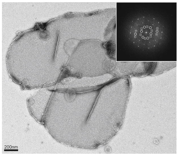
Negatively stained two-dimensional crystals of the galactose/H+ transporter GalP. The crystals are large and highly ordered. Inset, Fourier transform of the image shows strong and sharp spots to ∼18Å resolution. The crystals are vesicular and two sets of spots can be seen in the Fourier transforms (squares and circles). These crystals are suitable for analysis by cryo-EM and electron crystallography because the crystals are large and the spots in the Fourier transforms are sharp and extend to the resolution limit in negative stain. Figure adapted from (5).
Arguably the most critical step in cryo-EM is the preservation of the sample's finer structure. For electron crystallography, the crystalline vesicles or sheets must be frozen in such a way that preserves the crystalline order within the crystals. Even the very best 2D crystals will not diffract well if the crystals are not frozen properly in a hydrated state (discussed further in Subheading 3.3.1). Two methods are widely used: sugar embedding and vitrification. Our laboratory typically employs sugar embedding, and in the next section we describe the protocol for sample preparation by this method.
In the sugar embedding method, the 2D crystals are mixed with a sugar solution (Note 1) and then applied to an electron microscopy grid. Excess solution is blotted off and the sample is frozen (Fig. 2). The freezing can be done either slowly or very fast. Slow freezing is by far the easiest method. Here the blotted grid is placed into the cryo holder, then inserted into the electron microscope at room temperature, and viewed prior to freezing. An ideal grid should have very few broken grid windows. Each intact grid window should have ideally ten or more usable crystals, and the crystals should appear flat. One can tilt the stage to ∼40° to assess whether or not the carbon support is indeed flat. Any wrinkles in the carbon support will affect tilt data (Note 2). If the grid is intended for tilted data collection, it should be discarded if wrinkles are seen. Untilted data are not affected by micro-wrinkles, but grids with very large wrinkles should be discarded. The quality of the embedding is then assessed prior to freezing. A well-embedded crystal will exhibit strong and sharp reflections in power spectra, while a poorly embedded crystal will display smeared reflections, or no spots at all. From good crystals, one should expect to obtain strong reflections to at least ∼6Å resolution prior to freezing (Fig. 3). When such a preparation is encountered, liquid nitrogen (LN2) can be added to the dewar on the cryo holder. This will slowly freeze the grid at the cryoholder tip, a process that usually takes ∼30 min.
Fig. 2.
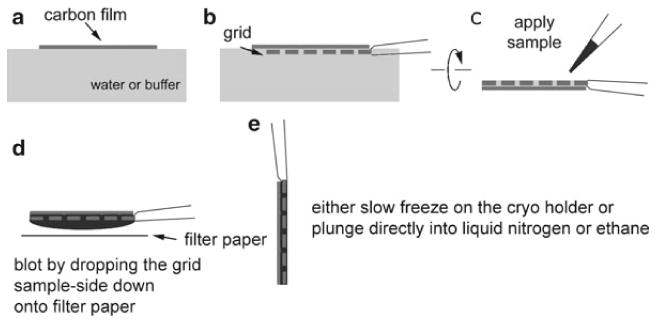
Preparation of the continuous carbon grid for cryo-EM. (a) A thin layer of carbon film evaporated onto mica is floated onto a glass petri dish filled with water or buffer of choice. The buffer can include the cryo protectant of choice such as trehalose, glucose, glycerol, etc. (b) The carbon is lifted onto an electron microscopy grid such as that composed of molybdenum or copper. (c) The tweezers are turned upside-down and the sample applied via pipette. The grid is then incubated for a few seconds at room temperature to allow the 2D crystals to settle and adhere to the carbon support. (d) The preparation is then turned upside-down and blotted directly by dropping the grid onto filter paper. At this stage one can control the eventual embedding by changing the blotting time. (e) When blotting is complete, the grid is picked up with tweezers and either placed onto the cryo holder for slow freezing or plunged into liquid nitrogen or liquid ethane for fast freezing.
Fig. 3.
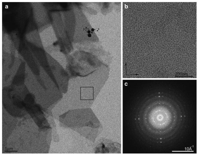
Cryo EM of two-dimensional crystals. (a) Crystals of the water channel aquaporin-0 are large and have sharp edges attesting to the degree of order within. (b) High-resolution image of the crystal area highlighted by a box in (a). (c) Fourier transform of the image in (b) showing strong and sharp spots to ∼6Å resolution. These crystals are ready for analysis by electron diffraction because the crystals appear uniformly grey on the grid. The spots in the Fourier transform are sharp and extend to ∼6Å resolution without unbending. At this stage the sample should be frozen and the microscope setup should be changed to diffraction and data collected.
Alternatively, with the fast-freeze method the blotted grid can be manually plunged into either LN2 or supercooled ethane immediately after blotting. The grid is then placed into a precooled cryo holder. The temperature of the cryo holder should be lower than −160°C, and preferably stabilized to lower than −180°C for longer than 5 min prior to insertion into the EM (Note 3). The sample preparation can then be viewed and assessed as above. This method is a little more cumbersome because ice buildup on the holder can be problematic, especially in very humid laboratories. Ice buildup can crash the vacuum on the microscope upon holder insertion.
3.1.1. Protocol for Sample Preparation
A thin layer of carbon is evaporated onto a layer of mica in a Cressington 208°Ccarbon evaporator in a vacuum greater than 2 × 10⁻⁶ Torr. An approximately 5 mm × 5 mm square of carbon-coated mica is then cut and floated onto a sugar solution, with the carbon facing up. The mica separates from the carbon leaving behind a thin layer of carbon floating on the water surface (Fig. 2a). An EM grid, grasped on its edge by a pair of anti-capillary tweezers, is then used to pick up the carbon (Fig. 2b). The grid is then turned over and the sample applied directly onto the grid (Fig. 2c). Excess solution is blotted off by dropping the grid face-down onto a piece of filter paper (Fig. 2d). The blotting time can be assayed but a good starting point is 10 s. The grid is then picked up with a pair of tweezers and either cooled in the EM using the slow method or directly plunged into LN2 or supercooled ethane (Fig. 2e) (Note 4).
3.2. Setup of the Electron Microscope for ED and Data Collection
Most of the data in our laboratory are collected using low-dose electron diffraction on an FEI Tecnai TF20 (200 kV cryo-TEM equipped with an FEG). Low-dose features three settings: search, focus, and exposure (10). The search mode is set as an overfocused diffraction mode allowing the user to examine a relatively large grid area with very little radiation damage to the sample. The beam is set to the smallest possible spot size (on our microscope it is spot size 11). The focus is identified and then overfocused from there to yield a highly contrasted image. Focus mode is an imaging mode (not diffraction) and done at 250,000× magnification at the specimen level. Exposure is in diffraction mode typically using a very small spot size such as 9 or 10. The focus mode is only used once or twice in a session for untilted specimens. For tilted specimens, it is recommended to refocus and realign directly adjacent to the target crystal prior to every ED collected.
When a crystal is identified the Selected Area aperture is inserted in the search mode and diffraction recorded in the exposure mode. The SA aperture is centered over a flat area of the crystal, and data that are recorded will only originate from the area of the crystal that was selected by the SA aperture. Because a small spot size is used, in addition to a small SA aperture, the electron count is quite low. As a result, diffraction data must be recorded over tens of seconds, typically up to 60 s.
Setup of the microscope for diffraction (Note 5):
Setting up the search mode:
Choose the smallest spot size.
Set magnification in imaging mode to ∼15,000×.
Turn diffraction on.
Change the diffraction length to the largest setting (e.g., 6,000 mm).
Focus the beam until you obtain a very sharp spot at the very center of the screen.
If the spot is not sharp, use the diffraction astigmators to sharpen the spot.
At the end of this procedure (if done properly) the beam should appear as a triangle with a sharp spot at its very center.
Overfocus the beam until an image appears on the screen.
Setting up focus mode (Note 6):
In search mode use the wobbler to find the eucentric Z-height.
Switch to focus mode.
Choose spot size 10.
Magnification should be set to 250,000×.
Set up the distance to ∼1.5 μm from the target.
Focus the beam crudely at first by using the eucentric focus feature.
Focus the beam more finely.
Reset focus when the focus is reached (do not defocus at this stage).
Setting up exposure mode:
Choose spot size 10.
Magnification should be set to ∼15,000×.
Spread the beam to ∼2 cm diameter on the viewing screen.
Turn diffraction on.
Choose the appropriate diffraction length (see Subheading 3.3.3).
Focus the beam until you get a sharp spot at the very center.
If the spot is not sharp, use the diffraction astigmators to sharpen the spot.
Insert the beam stopper (Subheading 3.3.2).
Use diffraction shift to align the diffraction beam with the beam stopper (Subheading 3.3.2).
Insert the CCD and record an image to determine the appropriate exposure time (Subheading 3.3.4).
Data collection in ED:
Find a crystal that appears flat and not folded in search mode.
Place the chosen crystal area at the center of the screen.
Insert the SA aperture and center the SA aperture over the chosen crystal area.
Insert the beam stopper (see Subheading 3.3.2).
Blank the beam.
Switch to exposure mode.
Raise the screen and cover the camera chamber with the rubber cover that was supplied with the microscope.
Unblank the beam.
At this stage the CCD is controlling the shutter, so the crystal is not exposed to radiation damage.
Record the diffraction using the appropriate exposure time (Subheading 3.3.4).
Once the diffraction is recorded, retract the camera.
Lower the screen.
Realign the beam behind the beam stopper.
Remove the beam stopper.
Check the beam for focus and diffraction astigmatism.
Remove the SA aperture.
Return to search mode.
Use the diffraction shift to align the exposed area of the crystal with the center of the screen.
Go back to step 1 above and repeat the process for collecting ED data of the next crystal.
3.3. Optimization of ED Data Collection
In this section we discuss specific items that need to be optimized for every ED experiment. When conditions for data collection are optimized, the obtainable resolution is far better. We begin by discussing specimen embedding and common problems with crystal flatness, and how to detect these during the ED experiment (Subheading 3.3.1). Next we discuss how the beam stopper is aligned so that maximum information is obtained (Subheading 3.3.2). We discuss the selection of diffraction length as a function of obtainable resolution (Subheading 3.3.3) and the selection of exposure time/saturation of the CCD (Subheading 3.3.4).
3.3.1. Assessment of Crystal Flatness and Embedding by Electron Diffraction
Optimum samples for ED are embedded properly in a cryoprotectant, and the crystals also lay flat against the carbon support. This allows accurate intensities to be recorded and subsequently measured. It is important to identify early in the ED experiment if the crystals are properly embedded, and if the preparation is sufficiently flat. Otherwise hours can be spent on the collection of suboptimal data.
An important objective of sample preparation for analysis by cryo-EM is to ensure the complete preservation of the finer structure of crystals in the sample. This is done by embedding the crystals in a thin layer of a cryoprotectant, as described in Subheading 3.1. Once the grid is prepared and the crystals behave as presented in Fig. 3, the user can set up the microscope for ED and begin recording electron diffraction data according to the protocol in Subheading 3.2.
It is advisable to first record diffraction patterns from untilted crystals to assess the overall quality of the preparation. The best data are always obtained from untilted crystals because these data are not affected by crystal flatness. Indeed, for well-ordered 2D crystals, if quality data are not obtained from untilted crystals the problem is almost certainly from the embedding and cryo preservation of the sample. In such cases, a new grid must be prepared. Once the diffraction from untilted crystals exhibits intense and sharp spots to high resolution, the user can then tilt the stage to 40–60° to assess grid flatness prior to data collection.
There are distinct features one can seek in the electron diffraction patterns of highly tilted crystals that can expedite the identification of flatness and/or embedding issues. Examples are presented in Fig. 4. The tilt axis is indicated as a dashed line. Any data along this line represent information at low tilt angle. The quality of data along the tilt axis provides information about crystal embedding. When a crystal is optimally embedded, spots along the tilt axis will be strong and sharp. The tilt data can be found perpendicular to the tilt axis, represented by a solid line in Fig. 4. Data along this axis provide information about crystal flatness. When the crystal is perfectly flat, the spots along this axis will be strong and sharp. With such information in hand, one can immediately identify when a crystal is both poorly embedded and not flat (Fig. 4a). If more than 20 consecutive crystals provide this sort of information, it is advisable to prepare a new grid and modify the embedding conditions. Using the guidelines above it is also straightforward to distinguish between crystals that are flat but poorly embedded (Fig. 4b) and crystals that are not flat yet embedded well (Fig. 4c). Crystals that are flat but poorly embedded will have sharp diffraction spots along both axes but the spots will not appear strong (Fig. 4b). Crystals that are not flat but are embedded well will have strong spots in all directions. The spots along the tilt axis will appear sharp but the ones perpendicular to the tilt axis will appear smeared (Fig. 4c). Finally, when the perfect grid is obtained the diffraction spots will appear strong and sharp, both on the tilt axis and in the direction perpendicular to the tilt axis (Fig. 4d).
Fig. 4.
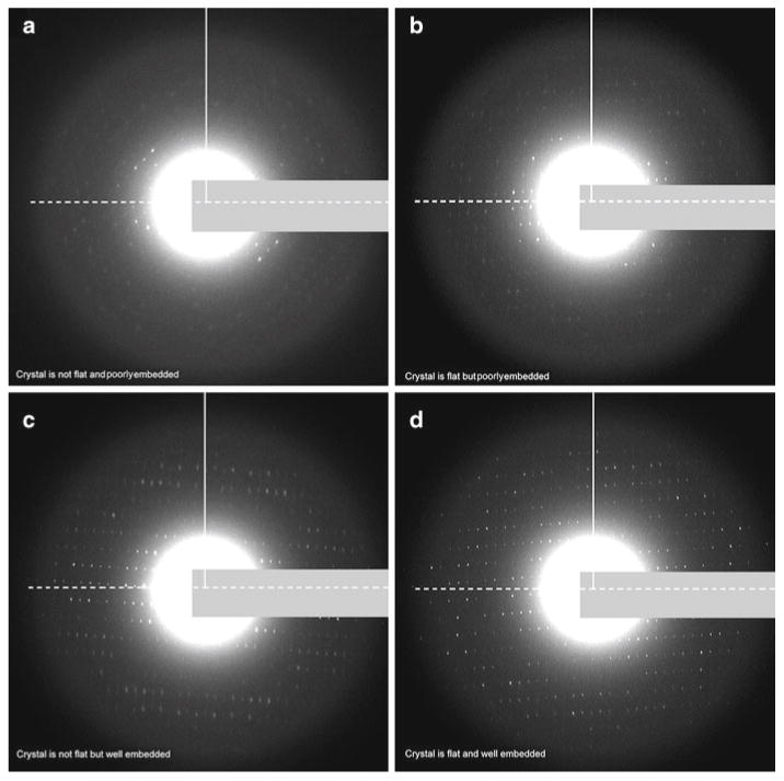
Assessment of crystal flatness and embedding by electron diffraction. (a–d) The flatness of the crystal will affect the attainable resolution. If crystals are not flat the resolution will be cut off in the direction perpendicular to the tilt axis (tilt axis in dashed line, perpendicular to the tilt axis in solid line). Likewise, a well-embedded crystal will show strong and sharp spots in the diffraction pattern but a poorly embedded crystal will have limited resolution. (a) An example of a crystal that is not flat and also poorly embedded. No sharp spots are visible perpendicular to the tilt axis, indicating that this crystal is not flat. Only a limited number of spots are visible on the tilt axis, indicating that the crystal is not embedded properly and was damaged during grid preparation. (b) An example of a crystal that is flat but poorly embedded. It is flat because many spots are visible in all directions, even perpendicular to the tilt axis. The crystal, however, is poorly embedded because most of the spots are not sharp and have a weak intensity. (c) An example of a crystal that is not flat but is embedded well. The crystal is well embedded because most spots in the diffraction patters appear strong. However, the crystal is not flat because only the spots on the tilt axis are sharp, while the spots perpendicular to the tilt axis are smeared. (d) An example of a crystal that is both flat and well embedded. All of the spots in this diffraction pattern are intense and sharp. In all figures the beam stop is masked by the grey rectangle.
3.3.2. Alignment of the Beam with the Beam Stop and with the CCD
When an optimal grid is obtained one must ensure that all possible data are recorded, and none are lost to simple alignment issues. There are three things that need to be perfectly aligned with respect to one another: the beam, the beam stop, and the center of the CCD (Note 7). The beam stop must be directly in front of the central beam. In electron diffraction the intensity of the central spot is much larger than all of the diffracted spots, so it is important to protect the CCD from overexposure and saturation that can cause bleeding and damage. The alignment of the central beam with the beam stop therefore ensures that the beam stop will protect the CCD from damage. The beam and the beam stop then need to be placed at the center of the recordable area of the CCD so that all possible information will be recorded evenly in all directions. Common alignment problems are illustrated in Fig. 5. In the first two examples, the beam (indicated by ×) and the beam stop are well aligned with respect to one another, but not with the recordable area of the CCD. In the first example the beam and the beam stop are too far to the right and information is lost on the x-axis (Fig. 5a). In the second example the beam and the beam stop are aligned too far to the top and information is lost in the y-axis (Fig. 5b). The beam can be centered in respect to the CCD by using diffraction shift, while the beam stop can be centered using the manual controls on the microscope. In Fig. 5c, both the beam and the beam stop are roughly at the center of the recordable area of the CCD but the beam is not aligned with the beam stop. As a result, the CCD is oversaturated and “bleeding” is observed. The diffraction shift can then be used again to center the beam behind the beam stop for perfect alignment, as presented in Fig. 5d.
Fig. 5.
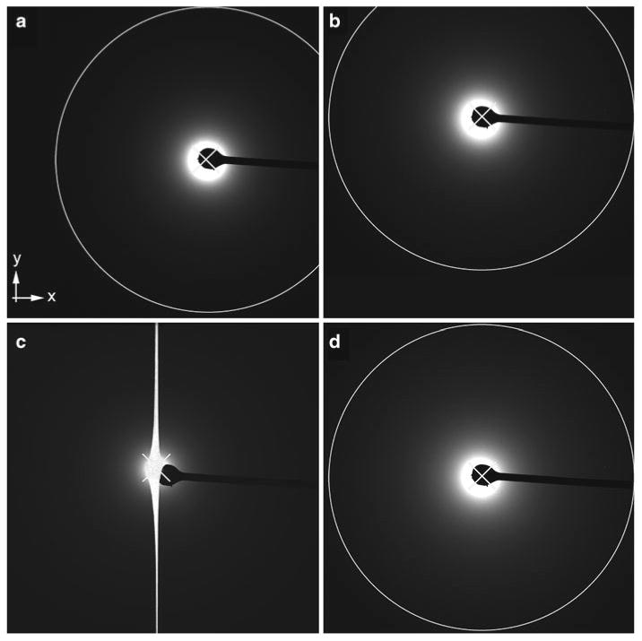
Alignment of the beam with the beam stop and with the CCD. It is important to align all three elements well; the beam must be at the center of the recordable area of the CCD so that no information will be lost, and the beam stop must be aligned with the beam to prevent damage to the CCD. (a and b) An example of a beam (indicated by an “x”) that is well aligned with the beam stop. The beam, however, is not at the center of the recordable area of the CCD and information on the x-axis or the y-axis is lost (a and b, respectively). (c) An example where the beam is aligned roughly at the center of the recordable area of the CCD but is not aligned with the beam stop. As a result the CCD is oversaturated and bleed-through in the y-axis is observed. (d) Perfect alignment. The beam is at the center of the recordable area of the CCD and directly behind the beam stop. Data to the same resolution can be recorded in all directions as indicated by the circle. In all panels the white X marks the center of the beam.
3.3.3. Selection of Diffraction Length
Another critical factor to consider in an ED experiment is the selection of the diffraction length (Note 8). Once the beam and the beam stop are aligned with the center of the recordable area of the CCD, one must select the correct diffraction length to optimize the quality of the obtainable data. The larger the diffraction length the lower the recordable resolution; however, the spaces between diffraction spots become larger, which facilitates indexing and background subtraction during data processing. Figure 6 illustrates three examples of diffraction data collected from aquaporin-0 2D crystals with three different camera lengths. The white circle indicates the resolution cutoff. Using the 4,000 mm diffraction length, the attainable resolution is ∼10Å (Fig. 6a). The diffraction spots are well separated, and accurate intensities can be extracted. However, it is clear that the crystals can diffract to even higher resolution because there are some strong and sharp spots that extend all the way to the edge of the recordable area of the CCD.
Fig. 6.
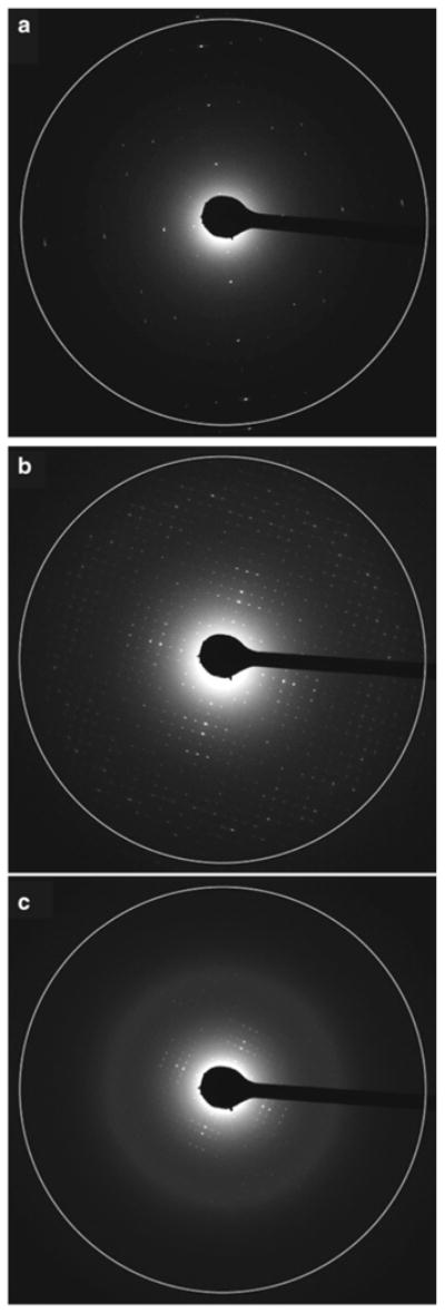
Selection of diffraction length. As with X-ray crystallography, the diffraction length in electron diffraction influences the attainable results. The longer the length, the lower the recordable resolution is. (a–c) Electron diffraction patterns recorded from untilted aquaporin-0 2D crystals with 4,000 mm, 3,000 mm, and 1,750 mm diffraction length lenses, respectively. The attainable resolution is 10Å, 3Å, and 1.5Å, respectively, as indicated by the white circle. As the camera length changes the diffraction spots also spread apart or condense. In this particular example the 3,000 mm lens is the ideal one to use because these particular crystals do not appear to diffract significantly better than 3Å under these embedding conditions. Data are therefore lost in (a) and no additional data are gained in (c).
The resolution cutoff becomes ∼3Å when the 3,000 mm diffraction length is used (Fig. 6b). The diffraction spots appear much closer together but are still separated enough to allow accurate determination of the intensities. No spots are visible at the edge of the recordable area of the CCD. The attainable resolution limit is ∼1.5Å when the 1,750 mm diffraction length is used (Fig. 6c). The spots appear much closer together, rendering indexing and intensity estimation difficult. Diffraction spots do not extend all the way to the edge of the white circle, so nothing is gained by changing the camera length from 3,000 to 1,750 mm. It is recommended to consider the camera length very carefully so that the best resolution is obtained and the extracted intensities are accurate. In the example presented here, the 3,000 mm diffraction length is ideal because the spots are well separated yet do not extend to the edge of the CCD, so no information is lost (Fig. 6b).
3.3.4. Optimization of Electron Dose and CCD Saturation in Electron Diffraction
A final consideration is electron dose and CCD saturation. When the electron dose is high, the CCD is saturated and accurate determination of spot intensities from diffraction patterns becomes impossible, thus rendering data useless. On the other hand, if the dose is low the beam becomes very weak and background noise increases, so the determination of spot intensity yet again becomes difficult. Moreover, high-resolution data that usually appear as weak spots may vanish in the high noise.
Different CCD cameras have different saturation points that the manufacturer should be able to provide upon request. However, these saturation points can, and should, be determined experimentally during setup of the electron beam prior to ED data collection. Once the beam is set up for diffraction and is aligned with the beam stop and with the CCD, one should record an exposure over 1 s, as illustrated in Fig. 7a. The intensity can then be displayed as a plot of counts versus distance (Fig. 7a, Inset). A dose that is not oversaturated will appear as a Gaussian curve. In this particular example, however, the counts are very low and the background noise is rather high. Without adjusting the beam settings one can increase the dose by increasing the exposure to 30 s or longer (Fig. 7b). Now the background appears more uniform and the counts are quite high, yet the CCD is not oversaturated and the dose plot still appears as a Gaussian curve (Fig. 7b, Inset). When the exposure is increased to 60 s the CCD is clearly oversaturated, as bleeding is observed. The dose plot here no longer appears Gaussian. In these examples the ideal setting was 30 s, as in Fig. 7b.
Fig. 7.
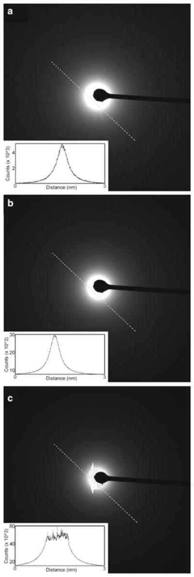
Optimization of electron dose and CCD saturation in electron diffraction. (a–c) The intensity over the line drawn is presented in the inset as counts versus distance. (a) Undersaturation. The beam is weak and as a consequence the background is noisy. The peak intensity inset is symmetric but appears noisy and is below the saturation, as indicated by the low counts. (b) Optimal dose. The peak intensity inset appears symmetric and has high counts. (c) Oversaturation. The peak intensity is too high and the CCD is oversaturated. No accurate intensities can be obtained with such settings.
4. Notes
Any number of sugars and sugar combinations can be assayed. A good starting point is 3–20% glucose or 3–20% trehalose.
Molybdenum grids are recommended for tilted data collection. Molybdenum shrinks less at low temperatures than copper, resulting in fewer micro-wrinkles on the carbon support. Copper grids are acceptable for untilted data collection.
Ensure that a beam is visible before inserting a cryo grid into the microscope. This makes it easy to distinguish problems with too thick ice (that result in the beam not being visible) from problems with the alignment or the electron source.
The double-carbon, or carbon-sandwich, technique (11) is described in detail elsewhere in this volume.
You will need to repeat this entire process three to four times because of hysteresis. Once the optics are stable, there should not be much variation as one changes from search to focus to exposure.
For data collection from untilted specimens the focus is only used once per grid. For tilted specimens repeat the entire procedure with focus before performing ED on every single crystal.
The SA also needs to be aligned with the beam, the beam stop, and the center of the CCD. See also Subheading 3.3.4—optimization of beam intensity.
The intensity and exposure time are affected by the size of the SA that is used. The larger the SA, the higher the dose at a constant exposure time.
Acknowledgments
We thank Noah Shuart (University of Washington) for critically reading this manuscript. Research in the Gonen laboratory is supported by the American Diabetes Association Award # 1-09-CD-05 and by the National Institutes of Health R01GM079233 and U54GM094598 as well as the Howard Hughes Medical Institute.
References
- 1.Henderson R, Unwin PN. Three-dimensional model of purple membrane obtained by electron microscopy. Nature. 1975;257:28–32. doi: 10.1038/257028a0. [DOI] [PubMed] [Google Scholar]
- 2.Andrews S, Reichow SL, Gonen T. Electron crystallography of aquaporins. IUBMB Life. 2008;60:430–436. doi: 10.1002/iub.53. [DOI] [PMC free article] [PubMed] [Google Scholar]
- 3.Reichow SL, Gonen T. Lipid-protein interactions probed by electron crystallography. Curr Opin Struct Biol. 2009;19:560–565. doi: 10.1016/j.sbi.2009.07.012. [DOI] [PMC free article] [PubMed] [Google Scholar]
- 4.Miyazawa A, Fujiyoshi Y, Unwin N. Structure and gating mechanism of the acetylcholine receptor pore. Nature. 2003;423:949–955. doi: 10.1038/nature01748. [DOI] [PubMed] [Google Scholar]
- 5.Zheng H, Taraska J, Merz AJ, Gonen T. The prototypical H+/galactose symporter GalP assembles into functional trimers. J Mol Biol. 2010;396:593–601. doi: 10.1016/j.jmb.2009.12.010. [DOI] [PMC free article] [PubMed] [Google Scholar]
- 6.Murata K, Mitsuoka K, Hirai T, Walz T, Agre P, Heymann JB, Engel A, Fujiyoshi Y. Structural determinants of water permeation through aquaporin-1. Nature. 2000;407:599–605. doi: 10.1038/35036519. [DOI] [PubMed] [Google Scholar]
- 7.Gonen T, Sliz P, Kistler J, Cheng Y, Walz T. Aquaporin-0 membrane junctions reveal the structure of a closed water pore. Nature. 2004;429:193–197. doi: 10.1038/nature02503. [DOI] [PubMed] [Google Scholar]
- 8.Gonen T, Cheng Y, Sliz P, Hiroaki Y, Fujiyoshi Y, Harrison SC, Walz T. Lipid-protein interactions in double-layered two-dimensional AQP0 crystals. Nature. 2005;438:633–638. doi: 10.1038/nature04321. [DOI] [PMC free article] [PubMed] [Google Scholar]
- 9.Ho JD, Yeh R, Sandstrom A, Chorny I, Harries WE, Robbins RA, Miercke LJ, Stroud RM. Crystal structure of human aquaporin 4 at 1.8 A and its mechanism of conductance. Proc Natl Acad Sci USA. 2009;106:7437–7442. doi: 10.1073/pnas.0902725106. [DOI] [PMC free article] [PubMed] [Google Scholar]
- 10.Fujiyoshi Y. The structural study of membrane proteins by electron crystallography. Adv Biophys. 1998;35:25–80. doi: 10.1016/s0065-227x(98)90004-1. [DOI] [PubMed] [Google Scholar]
- 11.Gyobu N, Tani K, Hiroaki Y, Kamegawa A, Mitsuoka K, Fujiyoshi Y. Improved specimen preparation for cryo-electron microscopy using a symmetric carbon sandwich technique. J Struct Biol. 2004;146:325–333. doi: 10.1016/j.jsb.2004.01.012. [DOI] [PubMed] [Google Scholar]


