Abstract
The present paper describes the results related to the optical and electrochemical characterization of thin carbon films fabricated by spin coating and pyrolysis of AZ P4330-RS photoresist. The goal of this paper is to provide comprehensive information allowing for the rational the selection of the conditions to fabricate optically-transparent carbon electrodes (OTCE) with specific electro-optical properties. According to our results, these electrodes could be appropriate choices as electrochemical transducers to monitor electrophoretic separations. At the core of this manuscript is the development and critical evaluation of a new optical model to calculate the thickness of the OTCE by variable angle spectroscopic ellipsometry (VASE). Such data was complemented with topography and roughness (obtained by AFM), electrochemical properties (obtained by cyclic voltammetry), electrical properties (obtained by electrochemical impedance spectroscopy), and structural composition (obtained by Raman spectroscopy). Although the described OTCE were used as substrates to investigate the effect of electrode potential on the real-time adsorption of proteins by ellipsometry, these results could enable the development of other biosensors that can be then integrated into various CE platforms.
Keywords: Carbon, Electrochemical, Optical, OTCE
1. Introduction
Among other materials that have been used to develop electrochemical and opto-electrochemical systems [1-3], carbon-based materials offer significant advantages towards the design of analytical applications [4]. Although the reasons for the selection of one particular allotrope over another are largely influenced by experience and cost, a variety of carbon-based materials [4, 5] are currently available. Besides offering good electrical conductivity, low background currents, and the possibility to catalyze pertinent reactions [6], nanostructured carbon-based materials display a unique density of functional groups [7], can promote the attachment of biorecognition elements, and can enhance the electron transfer rate, in some cases even with a direct transfer process [8-14]. Though not typically considered among those having unique properties resulting from the presence of nanosized features, thin carbon films (in the nm range) offer remarkable advantages with respect to more traditional materials. It is also important to highlight that these carbon-based films are transparent (due to the thickness) [15, 16], amenable to standard microfabrication procedures [17, 18], and allow tailoring their properties by selecting the appropriate starting material [19] and/or fabrication conditions [1, 20]. Furthermore, these electrodes (typically referred to as optically-transparent carbon electrodes, OTCE) are valuable for a number of applications ranging from basic spectroelectrochemical research to top-end technological applications involving light-emitting diodes and photovoltaic cells [21]. Furthermore, due to their optical and electrochemical properties OTCE could enable the integration separation science with multiple detection schemes, including optical, electrochemical, and spectroelectrochemical [17, 22, 23]. Such versatility is key to the integration of OTCE with CE and microchip-CE and the development of additional applications [17, 22] and integration procedures [24, 25].
An extensive body of literature related to the fabrication [15, 19, 26] and characterization [1, 16, 27, 28] of OTCE is currently available. However, most of these studies have focused on either the optical (mostly in the visible region of the electromagnetic spectrum) or electrochemical properties of OTCE. Aiming to provide rational guidelines for the development of OTCE, this manuscript provides a comprehensive description of the optical and electrochemical properties of these electrodes. In order to allow other researchers to build upon the results presented in this manuscript, standard materials and fabrication procedures were selected. In order to demonstrate their potential application, selected electrodes were then used to investigate the adsorption process of proteins upon the application of an electric field. These results could enable the development of biosensors that can be then integrated into various CE platforms.
2. Materials and Methods
Reagents and Solutions
Optically transparent carbon electrodes were fabricated by spin coating and pyrolysis of photoresist (AZ P4330-RS, AZ Electronic Materials USA Corp; Somerville, NJ). In order to control the thickness of the electrodes, dilutions of the commercial photoresist were prepared with propylene glycol monomethyl ether acetate (PGMEA, 99% Alfa Aesar; Ward Hill, MA) at a concentration of 20, 40, 60, 80, or 100% v/v of the as-received material. In all cases, the photoresist (and the corresponding dilutions) was stored in the dark until use. Aqueous solutions used to perform electrochemical experiments were prepared using 18 MΩ·cm water (NANOpure Diamond, Barnstead; Dubuque, IA) and analytical-grade reagents. Sulfuric Acid (ACS/FCC, BDH ARISTAR, 95.0-98.0%) was purchased from VWR (Pittsburgh, PA). Potassium hexacyanoferrate (III) and bovine serum albumin (BSA) were obtained from Sigma-Aldrich (Saint Louis, MO).
Fabrication of the OTCE
OTCE were prepared using either <111> silicon wafers (Si/SiO2, Sumco; Phoenix, AZ) or quartz glass slides (Technical Glass Inc., Painesville, OH) as substrates. The wafers were initially scored using a computer-controlled engraver (Gravograph IS400, Gravotech; Duluth, GA) and then manually cut. The process defined silicon substrates of 1 cm in width and 3 cm in length and square quartz substrates of 2.5 cm × 2.5 cm that were then cleaned by immersion in piranha solution (30% hydrogen peroxide and 70% sulfuric acid) at 90 °C for 30 min. After thorough rinsing, the substrates were stored in ultrapure water until use. In order to coat the substrates, a procedure developed by Donner et al [15] was slightly modified and used. Briefly, the clean substrates were first dried at 80 °C for 30 min and then placed in the spin coater (WS-400-6NPP, Laurel Technologies; North Wales, PA). Next, the atmosphere of the spin-coater chamber was saturated with PGMEA. Preliminary experiments showed that this step avoids the rapid evaporation of the solvent in the film during the coating process, yielding more uniform films. Then, 1 mL of the corresponding solution of photoresist was dispensed on the substrate and spun at 6000 rpm for 30 s. The substrates were then placed in a convection oven to evaporate the solvent at 110 °C for 60 s, and finally transferred to a tube furnace (Thermolyne F21135, Barnstead International; Dubuque, IA) for carbonization. In order to avoid combustion reactions that could ultimately remove all carbon from the surface, the pyrolysis step began by flushing the system with the forming gas (5% H2 / 95% Ar) at 1 L·min−1 for 5 min at room temperature. Next, the temperature was increased to 1000 °C using a ramp of 20 °C·min−1. The temperature was held at 1000 °C for 1 h while the forming gas was flowing continuously at 1 L·min−1 through the quartz tube. Finally, the system was allowed to cool down back to room temperature, maintaining a constant flow of forming gas. The OTCE were stored before use in a Petri dish for a minimum of 3 days to allow stabilization of the surface by spontaneous oxidation [15]. Electrical contact to the OTCE was achieved by sputtering a gold contact (60 sec at 0.2 mA, Cressington 108 Auto; Watford, England). Finally, a standard copper wire was fixed to the OTCE with a drop of silver paint (SPI Supplies; West Chester, PA). For all experiments, electrodes of 1 cm x 1 cm were defined by either wrapping the electrode with Teflon tape or applying an insulating spray (cat. # 422, MG Chemicals).
Spectroscopic Ellipsometry (SE) and Transmittance (T)
Ellipsometry is an optical technique that measures changes in the reflectance and phase difference between the parallel (RP) and perpendicular(RS) components of a polarized light beam upon reflection from a surface. Using Equation 1, the intensity ratio of RP and RS can be related to the amplitude ratio (tan (Ψ)) and the phase difference (∆) between the two components.
| Equation 1 |
Therefore, ellipsometry can be used to determine the optical properties (index of refraction (n) and extinction coefficient (k)) and film thickness (d) of both single- and multi-layer systems. Ellipsometric and transmittance experiments were performed using a variable angle spectroscopic ellipsometer (WVASE, J.A. Woollam Co.; Lincoln, NE) following a procedure described elsewhere [29-32]. The experimental results were then interpreted using an ad-hoc optical model, also developed using the WVASE software package (J.A. Woollam Co.; Lincoln, NE). The model (that describes the substrate microstructure in terms of n, k, and d) consisted in three uniaxial layers with optical axes parallel to the substrate surface. The dielectric functions of each layer were described by a layer of Si (bulk; d = 1 mm), a layer of SiO2 (d = 2.1 ± 0.5 nm), and a layer of carbon. The optical constants of the latter were calculated from a combination of transmittance and ellipsometric experiments, also carried out using the WVASE system. The accuracy between the experimental and model-general data was evaluated using the mean square error (MSE) [33], a built-in function in WVASE based on Equation 2,
| Equation 2 |
where N is the number of Ψ and ∆ pairs used in the measurement, M is the number of parameters varied in the regression analysis, and σ is the standard deviation of the experimental data points. In agreement with previous reports [34, 35], MSE < 15 were considered acceptable.
Atomic Force Microscopy (AFM)
AFM was used to verify the thickness of the OTCE and evaluate the topography of the substrates. Experiments were performed using a Veeco diMultimode Nanoscope V scanning probe microscope operating in tapping and non-contact mode. The thickness of the OTCE layer was measured by performing a depth profile of a groove created by removing a portion of the carbon film with a scalpel.
Raman Spectroscopy
A confocal Raman automated imaging spectrometer (iHR320, Horiba Jobin Yvon) was used to study the molecular morphology of the OTCE. The Raman spectrometer was equipped with a Synapse CCD detector, with 785 nm wavelength of the excitation laser. The Raman spectra were collected in the 800-2000 cm−1 range, with an exposure time of 2 sec, an accumulation factor of 2, and with a 100X objective.
Electrochemical techniques
Cyclic voltammetry (CV) was used to investigate the electrochemical performance of the OTCE. Experiments were performed using 100 mmol·L−1 H2SO4 as supporting electrolyte and 1.0 mmol·L−1 Fe(CN)63−/Fe(CN)64−, as the redox couple. All solutions were deoxygenated by bubbling N2 for at least 5 min. CV experiments were carried out using a CHI812 Electrochemical Analyzer (CH Instruments, Inc.; Austin, TX), a silver/silver chloride (Ag/AgCl, saturated KCl) reference electrode, and a platinum wire as the counter electrode. Electrochemical impedance spectroscopy (EIS) was used to investigate the evolution of the electrochemical properties of the OTCE and complement the information collected by CV. Impedance measurements were also performed using 1.0 mmol·L−1 Fe(CN)63−/Fe(CN)64− dissolved in 100 mmol·L−1 H2SO4 as supporting electrolyte, at −0.4 V and between 10−2 and 105 Hz. The applied potential was selected to maximize the faradaic current (under the selected experimental conditions). To determine the contribution of each electrical element, a Randles-type equivalent circuit (vide infra) was used and fit with the simulation software Zview-Impedance®, version 2.4a.
Safety considerations
The described procedure for the preparation of OTCEs involves the use of heat (1000 °C) and a mixture of 5% H2 / 95% Ar; consequently, should be carefully handled. Hydrogen can form a flammable mixture with air over a wide range of concentrations, and very low energy is needed to ignite hydrogen-air mixtures. Extreme care should be taken while handling the tube furnace, as the quartz may be very hot even though it is no longer glowing. Piranha solution (30% H2O2 and 70% sulfuric acid) is a strongly oxidizing cleaning solution used to remove organic residues from substrates. As such, piranha solution is extremely corrosive, reactive, and potentially explosive so that should be also carefully handled.
3. Results and Discussion
Thickness of the OTCE
As it generally defines the transparency and electrical resistance of the OTCE, one of the critical parameters to investigate is the thickness of the formed films. In the experiments herein described, the thickness of the OTCE was controlled by using different dilutions of the selected photoresist in PGMEA. As the previous models [30, 31, 36-38] were not able to accurately describe the optical properties of the resulting OTCE (therefore precluding the calculation of the thickness by ellipsometry), the thickness of the substrates was initially investigated by AFM. Figure 1A shows a representative image of the film and the location of the groove used to calculate the thickness of the film.
Figure 1A.
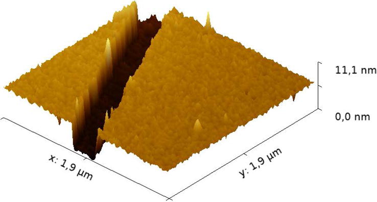
AFM micrograph of the OTCE fabricated by spin coating a 20% dilution of photoresist onto silicon wafers. The micrograph also shows the groove created to measure the thickness of the film by AFM.
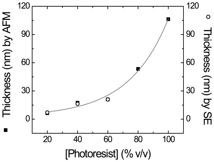
It is worth mentioning that at least five grooves were analyzed in each substrate, discarding those that did not reach the underlying Si/SiO2 substrate. As it can be observed in Figure 1B, increasing the concentration of the photoresist resulted in significant changes in the thickness of the electrodes. As expected, the thickness of the OTCE layer shows an exponential dependence with respect to the concentration of photoresist. It is also important to note that although preliminary experiments performed by SEM rendered similar thickness values, the limited precision of such measurements did not allow performing additional calculations.
Figure 1B.
Relationship between the thicknesses of carbon films (obtained by AFM and SE) versus the concentration of photoresist used to prepare the OTCE. Data points and error bars (contained within the points) represent the average and standard deviation, respectively, of at least five measurements.
AFM was also used to measure the topography of the surface of the OTCE. In agreement with previous reports, all images showed continuous structures of OTCE on the Si/SiO2 substrates, with abundant nanostructured features throughout the surface. The overall roughness of the surface was calculated to be ± 0.5 nm, for all the investigated films.
Resistance and Transmittance
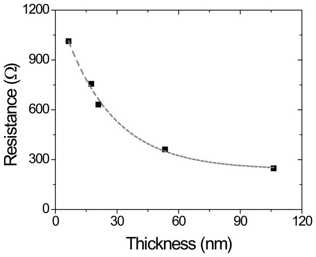
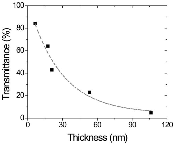
OTCE are interesting substrates in the field of adsorption science and nanotechnology because they enable performing both electrochemical and optical experiments. However, the film resistance and transparency must be carefully balanced. As previously reported, although thicker electrodes display lower resistance, significant decreases in transparency are often associated with thick films [15, 16, 28, 39, 40]. Therefore, and aiming to rationally select the most suitable OTCE for both electrochemical and ellipsometry measurements, the carbon films obtained were characterized in terms of resistance and optical transparency. The electrical behavior of OTCEs as a function of thickness was initially assessed by measuring the resistance of each carbon film between two gold contacts (sputtered with a 1 cm gap) using a standard multimeter (2-point probe). As can be observed in Figure 2A, a gradual decay in the resistance of the carbon films was observed as the film thickness increases, reaching 248 Ω for the OTCE fabricated with 100% photoresist (thickness = 106.2 ± 0.3 nm). This trend, which is good agreement with previous literature reports [41, 42], has been attributed to a progressive restriction of hopping conductivity (low temperature conduction in systems composed of localized and disordered domains) [15]. As previously stated, there is a trade-off between transparency and resistivity of the films. Consequently, the transparency of the electrodes was evaluated in the 200-1000 nm wavelength range using OTCE deposited on quartz substrates from different dilutions of the photoresist. All substrates showed a slight decrease in transmittance as the wavelength decreases, leading to a well-defined absorption peak at 250 nm (see Supplementary Information). Similar profiles have been previously reported for other carbon-based nanomaterials [21]. Figure 2B shows a summary of the overall trend observed, where the overall light transmittance of the substrates was significantly influenced by the thickness of the OTCE deposited.
Figure 2A.
Dependence of the resistance as a function of the thickness of the OTCE. Conditions as described in the Experimental section.
Figure 2B.
Dependence of the transmittance at 600 nm as a function of the thickness of the OTCE deposited on quartz glass slides. Other conditions as described in the Experimental section.
It is also worth noting that, under the conditions selected for the preparation of this OTCE, a linear relationship between the transmittance and the resistance was obtained (R(Ω) = 962.6 T(%) + 180), enabling the estimation of % transmittance from much simpler, electrical measurements.
Optical Characterization
In order to describe the optical behavior of the OTCE, the optical constants (n and k) of the film should be extracted. However, fitting for those parameters in thin films is rather challenging because the models tend to couple those parameters with the film thickness, potentially leading to wrong interpretations. Aiming to minimize the chances of obtaining an inaccurate set of optical constants, three independent approaches were applied to calculate the optical constants of the films. In all cases, the built-in WVASE software package (J.A. Woollam Co.; Lincoln, NE) was used to fit the experimental data and calculate the optical constants. In the first case, the optical properties of arc-evaporated carbon [36, 43] were used as reference material to fit the data obtained from the ellipsometric and transmittance experiments, performed on OTCE deposited on quartz substrates. It is worth noting that thicker films (> 30 nm, see Figure 2B) exhibited very low transmittance (< 30%), greatly reducing the signal/noise, and therefore precluding their analysis. Consequently, the optical properties of the selected films were modeled by a layer of SiO2 (bulk; d = 1 mm) and the layer of optically transparent carbon. Although the constants calculated by this method were in agreement with respect to those reported for other carbon films [41], they were only used as a first approximation to the model parameters.
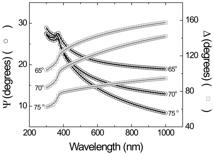
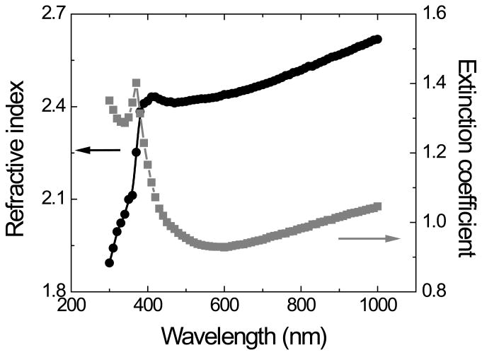
In the second approach, the spectroscopic ellipsometry data (Ψ and ∆ vs λ) obtained from films deposited in silicon wafers were used to refine the preliminary model obtained by the first approach. In this case, the model was composed of a layer of Si (bulk, d = 1 mm), a layer of SiO2 (d = 2.1 ± 0.5 nm), the layer of optically transparent carbon, and a fourth layer accounting for the roughness of the films (also observed by AFM). As it can be observed in Figure 3A, a good agreement (MSE < 10) between the experimental and the model-generated data was obtained. Such agreement allowed calculating the thickness of the OTCE and extracting the optical constants for the carbon layer (Figure 3B). This refined optical model should allow the calculation of the thickness of other OTCE fabricated under similar conditions. As it can be observed in Figure 1B, an excellent agreement (R2 = 0.99) was obtained between the thickness calculated by AFM and those values calculated by ellipsometry, further confirming the appropriateness of the model.
Figure 3A.
Dependence of the ellipsometric angles (Ψ and ∆) as a function of the wavelength (nm) of the incident light beam, collected at three different angles (as noted in the figure). Data points correspond to experimental data and lines correspond to model-generated values. Other conditions as described in the Experimental section.
Figure 3B.
Dependence of the refractive index (n) and extinction coefficient (k) of the films as a function of the wavelength (nm) of the incident light beam. Other conditions as described in the Experimental section.
The third approach used to calculate the optical constants of the OTCE consisted in feeding the model with the thickness values obtained by AFM and letting the optical constants fluctuate. This strategy yielded identical optical constants (data not shown) and was only used to confirm the results. It is also important to mention that the three selected approaches rendered similar results (within their corresponding errors) and were considered to be complementary with each other.
Microstructure of the Films
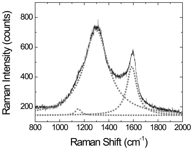
It is well known that carbon has several allotropes and can exist in a wide range of disordered forms. Raman spectroscopy was found to be sensitive to the presence of such structures and to changes that perturb the translational symmetry of the sample [44]. For this reason, Raman spectroscopy was used to obtain structural information related to the OTCE produced with different concentrations of photoresist. A representative example of the spectra obtained is shown in Figure 4. The results were then analyzed to calculate the intensity of the G band (at 1587 cm−1) and the D band (at 1296 cm−1), which have been attributed to the breathing of C-C bonds in graphite-like carbon (sp2) and the breakdown of such symmetry, respectively. Additionally, a shoulder at 1151 cm−1 assigned to the presence of nanocrystalline diamond phases (sp3 carbon) [45] was also observed. Therefore, the Raman spectra were deconvoluted into three Lorentzian [46] peaks centered at 1151 cm−1, 1296 cm−1, and 1587 cm−1. In agreement with previous reports performed under similar conditions (785 nm) [47], the D/Eg2 ratio was found to be (4.2 ± 0.1). This ratio, which has been previously reported for pyrolytic carbon substrates [48], suggests that the disorder of the layer could avoid the proper alignment of atomic orbitals of the graphene sheets and consequently preclude the formation of a large π-conjugated systems [49]. These results not only support the necessity of performing an accurate characterization of the films but also are in agreement with the previously-discussed electrical properties of the OTCE.
Figure 4.
Raman spectrum of OTCE produced with 100% of photoresist in PGMEA. Data line corresponds to experimental data and points correspond to deconvoluted Lorentzian peaks. Other conditions as described in the Experimental section.
Electrochemical Characterization
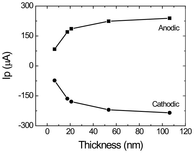
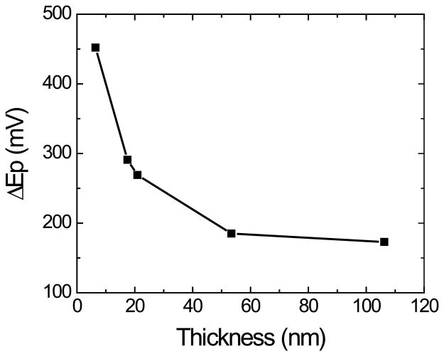
The electrochemical performance of the produced OTCE was initially studied by steady-state cyclic voltammetry. Experiments were performed in 100 mmol·L−1 H2SO4 solution, as supporting electrolyte, containing 1.0 mmol·L−1 K3Fe(CN)6/K4Fe(CN)6, as a model electrochemically-reversible redox couple. The working-potential window of the OTCE ranged (under normal operational conditions) from −0.6 V to 1.5 V, and it was slightly narrower than the value reported for other carbon electrodes [50]. In all cyclic voltammetry experiments (performed in the −0.4 / 1.2 V range), well-defined peaks for the oxidation and reduction of the redox couple were observed during the anodic and cathodic sweeps, respectively. Initially, the effect of the electrode thickness (which affects the resistance and transparency of the layer, see Figure 2) on the peak current (IP) and peak potential (EP) was investigated using a sweep rate of 50 mV·s−1. As it can be observed in Figure 5A, increasing the thickness of the OTCE resulted in systematic improvements in the peak current of both processes. The ratio between the anodic and cathodic IP showed only slight improvements, decreasing from 1.15 to 1.01 for the 6.5 nm and 106.2 nm OTCE, respectively. As shown in Figure 5B, increasing the thickness of the OTCE also decreased the peak potential difference, reaching a minimum of 173 mV, for the 106.2 nm OTCE. In agreement with Nicholson [51], this value (which is almost three times the ideal ∆Ep = 0.059 V/n), suggests that the oxidation and reduction process are not related and can be treated separately, just like any other irreversible process.
Figure 5A.
Dependence of the anodic and cathodic peak current (lp) as a function of the thickness of the OTCE. Conditions as described in the Experimental section.
Figure 5B.
Dependence of the peak potential difference (∆Ep) as a function of the thickness of the OTCE. Conditions as described in the Experimental section.
Based on these results, and considering that the one of the advantages of the proposed substrates is the possibility to perform experiments coupling spectroscopic and electrochemical techniques, OTCE prepared from 40% and 60% dilutions of photoresists were considered more appropriate and further characterized. As a representative example, the results obtained with the OTCE prepared from the 60% dilution of photoresist in PGMEA (d = 20.9 nm, T = 43%, and R = 631 Ω) are herein discussed. For these experiments, the peak current and peak potential obtained from cyclic voltammograms performed at different scan rates (in the 10-200 mV·s−1 range, 1.0 mmol·L−1 K3Fe(CN)6/K4Fe(CN)6 in 100 mmol·L−1 H2SO4) are discussed. The results showed a linear dependence of both the peak current (anodic and cathodic) as well as the peak potential with respect to the square root of the scan rate (v1/2). However, the large ∆Ep and its dependence with respect to the scan rate (∆Ep(mV) = 13.3 v1/2 + 92.4) indicates a decreasing degree of reversibility as scan rates increase, approaching the limit for irreversible electrochemical behavior (ψ = 0) [52]. In order to confirm that these limitations can be attributed to the resistive nature of the OTCE films (IR drop); the effect of the concentration of the electroactive species was investigated. In this case, decreasing the concentration of K3Fe(CN)6/K4Fe(CN)6 from 1.0 mmol·L−1 to 0.5 mmol·L−1 produced a decrease in the anodic peak potential of 42 mV and an increase in the anodic peak potential of the same magnitude. These resistive effects are a common drawback of many carbon-based electrodes [53].
In order to characterize the prepared electrodes in terms of their electrical behavior, the OTCE prepared from the 60% dilution of photoresist in PGMEA (d = 20.9 nm, T = 43%, and R = 631 Ω) was investigated by electrochemical impedance spectroscopy. Figure 6 shows a representative example of a Nyquist plot obtained with the selected electrode.
Figure 6.
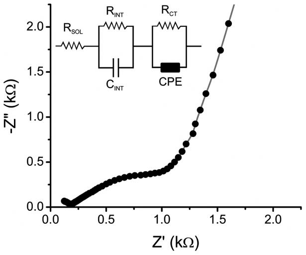
Nyquist plot obtained from OTCE prepared with 60% photoresist in PGMEA. Data points correspond to experimental data and line correspond to model-generated values. The insert show the equivalent circuit used to fit experimental data. Conditions as described in the experimental section.
In order to calculate the value of each component of the equivalent circuit, the spectrum was simulated with the equivalent circuit included in Figure 6 (see insert), where RSOL, RINT, RCT, and CINT corresponds to the resistance of the electrolyte, the internal resistance of the film, the charge-transfer resistance and the internal capacitance of the film. The circuit also included a constant phase element (CPE) with an exponent (α = 0.59 ± 0.01) in order to account for the roughness of the surface [54]. The values calculated for each element were: RSOL, kΩ = 0.18 ± 0.01, RINT, kΩ = 13.7 ± 0.6, RCT, kΩ = 1.24 ± 0.02, CINT, μf/s = 262 ± 1, and CPE μF/s = 0.71 ± 0.03. The quality of the fitting was evaluated using a built-in function in the software (% error < 5%), which was considered adequate. The difference between the values obtained under AC conditions and those obtained under DC conditions, suggests that the OTCE show the typical frequency dependence observed in other thin films [55, 56].
Adsorption of Bovine Serum Albumin (BSA)
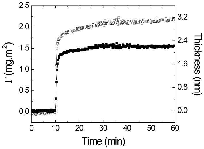
As previously discussed, the OTCE herein described were conceived as an alternative option towards the development of electrochemical biosensors. The particular importance of OTCE is that (besides being conductive, nanostructured, and uniform in terms of thickness) they enable the simultaneous use of optical and electrochemical techniques. Following previous papers from our group [30, 36, 38, 57, 58], it was considered important to investigate the adsorption of proteins at various the electrode surfaces. This information could lead to the rational development of biosensors with improved sensitivity. Although the development of biosensors is outside the scope of the present manuscript, the possibility of applying the OTCE for such experiments is herein demonstrated. For these experiments, a previously described procedure was followed [30, 36, 38, 57]. Briefly, the ellipsometry cell [59] was filled with buffer (10 mmol·L−1 phosphate buffer, pH = 4.7) and aligned. Solution was pumped through the cell for 10 min and the ellipsometric angles measured to establish the baseline. Then, a solution containing the selected protein was injected in the cell at a flow rate of 1 mL·min−1 until a plateau was observed (typically within 60 min). During that time, the ellipsometric angles (ψ and ∆) were measured as a function of time, using 500 nm as the incident wavelength. The collected data was then used to determine the thickness (d, expressed in nm) of the protein layer adsorbed to the OTCE. Finally, the amount of adsorbed BSA (Γ, expressed in mg·m−2) can be calculated using Equation 3,
| Equation 3 |
where n and no are the refractive index of the protein and of the ambient (aqueous buffer), respectively and dn/dc is the increment of refractive index for the proteins in the adsorbed layer. As a representative example, Figure 7 shows the dynamic adsorption experiment of BSA on the surface of the OTCE. As expected, a rather fast process was observed in both cases leading to the formation of a compact layer of protein on the surface of the OTCE. As it can also be observed in Figure 7, the containing either 1.54 ± 0.04 or 2.18 ± 0.04 mg·m−2 of BSA depending on the applied potential at the OTCE-solution interface (OCP and 650 mV, respectively). Experiments involving a wider selection of proteins and experimental conditions are currently underway and will be reported separately.
Figure 7.
Adsorption kinetic of 0.5 mg·mL−1 BSA on the OTCE fixed with 60% of photoresist at OCP (full square) and 650 mV (empty square). The experiment was performed in 10 mmol.L−1 phosphate buffer at pH = 4.7 and a flow rate of 1 mL·min.
4. Conclusions
Uniform thin carbon films of different thicknesses were obtained by pyrolysis of different dilutions of AZ P4330-RS photoresist coating silicon wafers. The electrodes were characterized by atomic force microscopy, cyclic voltammetry, electrochemical impedance spectroscopy and Raman spectroscopy. That information allowed the development of a simple model to describe the optical properties of both the OTCE and the subsequent protein layer, enabling other researchers to build upon this information. Furthermore, and as a balance between electrochemical properties and optical transparency, the carbon film prepared with 60% of photoresist was selected as the most appropriate substrate to investigate the effect of electrode potential on the adsorption of BSA. The obtained results demonstrate that the potential applied to the surface has a significant effect on the adsorption process (kinetics and saturation amount) of BSA. Finally, the wide operational potential window of these electrodes (from −0.6 V to 1.5 V) can be used to investigate the effect of the applied potential on the OTCE in the molecular adsorption processes as well as to bolster the development of other opto-electrical devices such as detectors for microchip devices.
Supplementary Material
Acknowledgments
Financial support for this project has been provided in part by the University of Texas at San Antonio and the National Institutes of Health through the National Institute of General Medical Sciences (2SC3GM081085) and the Research Centers at Minority Institutions (G12MD007591).
Footnotes
The authors have declared no conflict of interests.
References
- 1.Schreiber M, Lutz T, Keeley GP, Kumar S, Boese M, Krishnamurthy S, Duesberg GS. Appl Surf Sci. 2010;256:6186–6190. [Google Scholar]
- 2.Su M, Wei W, Liu S. Anal Chim Acta. 2011;704:16–32. doi: 10.1016/j.aca.2011.07.016. [DOI] [PubMed] [Google Scholar]
- 3.Szyszka B, Dewald W, Gurram SK, Pflug A, Schulz C, Siemers M, Sittinger V, Ulrich S. Curr Appl Phys. 2012;12(4):S2–S11. [Google Scholar]
- 4.Scida K, Stege PW, Haby G, Messina GA, Garcia CD. Anal Chim Acta. 2011;691:6–17. doi: 10.1016/j.aca.2011.02.025. [DOI] [PMC free article] [PubMed] [Google Scholar]
- 5.Kumar CSSR, editor. Carbon Nanomaterials. John Wiley & Sons, Inc; Weinheim, Germany: 2011. [Google Scholar]
- 6.Sanford AL, Morton SW, Whitehouse KL, Oara HM, Lugo-Morales LZ, Roberts JG, Sombers LA. Anal Chem. 2010;82:5205–5210. doi: 10.1021/ac100536s. [DOI] [PMC free article] [PubMed] [Google Scholar]
- 7.Roberts JG, Moody BP, McCarty GS, Sombers LA. Langmuir. 2010;26:9116–9122. doi: 10.1021/la9048924. [DOI] [PubMed] [Google Scholar]
- 8.Pumera M, Escarpa A. Electrophoresis. 2009;30:3315–3323. doi: 10.1002/elps.200900008. [DOI] [PubMed] [Google Scholar]
- 9.Vandaveer WR, Pasas-Farmer SA, Fischer DJ, Frankenfeld CN, Lunte SM. Electrophoresis. 2004;25:3528–3549. doi: 10.1002/elps.200406115. [DOI] [PubMed] [Google Scholar]
- 10.Vandaveer WRT, Pasas-Farmer SA, Fischer DJ, Frankenfeld CN, Lunte SM. Electrophoresis. 2004;25:3528–3549. doi: 10.1002/elps.200406115. [DOI] [PubMed] [Google Scholar]
- 11.Wang J. Electroanalysis. 2005;17:1133–1140. [Google Scholar]
- 12.Escarpa A, González MC, Crevillén AG, Blasco AJ. Electrophoresis. 2007;28:1002–1011. doi: 10.1002/elps.200600412. [DOI] [PubMed] [Google Scholar]
- 13.Crevillen AG, Pumera M, Gonzalez MC, Escarpa A. Lab Chip. 2009;9:346–353. doi: 10.1039/b809963d. [DOI] [PubMed] [Google Scholar]
- 14.Vilela D, Garoz J, Colina Á, González MC, Escarpa A. Anal Chem. 2012;84:10838–10844. doi: 10.1021/ac303049x. [DOI] [PubMed] [Google Scholar]
- 15.Donner S, Li HW, Yeung ES, Porter MD. Anal Chem. 2006;78:2816–2822. doi: 10.1021/ac052244d. [DOI] [PubMed] [Google Scholar]
- 16.Dai Y, Swain GM, Porter MD, Zak Jerzy. Anal Chem. 2008;80:14–22. doi: 10.1021/ac085996r. [DOI] [PubMed] [Google Scholar]
- 17.Hebert NE, Snyder B, McCreery RL, Kuhr WG, Brazill SA. Anal Chem. 2003;75:4265–4271. doi: 10.1021/ac026425g. [DOI] [PubMed] [Google Scholar]
- 18.Gonzalez CF, Cropek DM, Henry CS. Electroanalysis. 2009;21:2171–2174. [Google Scholar]
- 19.Matsuo Y, Iwasa K, Sugie Y, Mineshige A, Usami H. Carbon. 2010;48:4009–4014. [Google Scholar]
- 20.Kostecki R, Schnyder B, Alliata D, Song X, Kinoshita K, Kötz R. Thin Solid Films. 2001;396:36–43. [Google Scholar]
- 21.Weber CM, Eisele DM, Rabe JP, Liang Y, Feng X, Zhi L, Müllen K, Lyon JL, Williams R, Bout DAV, Stevenson KJ. Small. 2010;6:184–189. doi: 10.1002/smll.200901448. [DOI] [PubMed] [Google Scholar]
- 22.Fischer DJ, Vandaveer WR, Grigsby RJ, Lunte SM. Electroanalysis. 2005;17:1153–1159. [Google Scholar]
- 23.Hebert NE, Kuhr WG, Brazill SA. Anal Chem. 2003;75:3301–3307. doi: 10.1021/ac0262457. [DOI] [PubMed] [Google Scholar]
- 24.Ding Y, Ayon A, Garcia CD. Anal Chim Acta. 2007;584:244–251. doi: 10.1016/j.aca.2006.11.064. [DOI] [PubMed] [Google Scholar]
- 25.Johnson AS, Selimovic A, Martin RS. Electrophoresis. 2011;32:3121–3128. doi: 10.1002/elps.201100433. [DOI] [PMC free article] [PubMed] [Google Scholar]
- 26.Walker EK, Vanden Bout DA, Stevenson KJ. Langmuir. 2011;28:1604–1610. doi: 10.1021/la2042394. [DOI] [PubMed] [Google Scholar]
- 27.Henke L, Piunno PAE, Nagy N, Wust CC, Krull UJ. Anal Chim Acta. 2001;433:31. [Google Scholar]
- 28.Kummer M, Kirchhoff JR. Electroanalysis. 1996;8:524–528. [Google Scholar]
- 29.Mora MF, Giacomelli CE, Garcia CD. Anal Chem. 2009;81:1016–1022. doi: 10.1021/ac802068n. [DOI] [PMC free article] [PubMed] [Google Scholar]
- 30.Felhofer JL, Caranto J, Garcia CD. Langmuir. 2010;26:17178–17183. doi: 10.1021/la103035n. [DOI] [PMC free article] [PubMed] [Google Scholar]
- 31.Soetedjo H, Mora MF, Garcia CD. Thin Solid Films. 2010;518:3954–3959. doi: 10.1016/j.tsf.2010.02.037. [DOI] [PMC free article] [PubMed] [Google Scholar]
- 32.Wehmeyer J, Bizios R, Garcia CD. Mat Sci Eng C. 2010;30:277–282. doi: 10.1016/j.msec.2009.11.002. [DOI] [PMC free article] [PubMed] [Google Scholar]
- 33.Alterovitz SA, Johs B. Thin Solid Films. 1998:313–314. 124-127. [Google Scholar]
- 34.Barnes TM, van de Lagemaat J, Levi D, Rumbles G, Coutts TJ, Weeks CL, Britz DA, Levitsky I, Peltola J, Glatkowski P. Phys Rev B. 2007;75:23541001–22354110. [Google Scholar]
- 35.Shrestha RP, Yang D, Irene EA. Thin Solid Films. 2006;500:252–258. [Google Scholar]
- 36.Mora MF, Giacomelli CE, Garcia CD. Anal Chem. 2009;81:1016–1022. doi: 10.1021/ac802068n. [DOI] [PMC free article] [PubMed] [Google Scholar]
- 37.Carot ML, Torresi RM, Garcia CD, Esplandiu MJ, Giacomelli CE. J Phys Chem C. 2010;114:4459–4465. doi: 10.1021/jp9085359. [DOI] [PMC free article] [PubMed] [Google Scholar]
- 38.Nejadnik MR, Francis L, Garcia CD. Electroanalysis. 2011;23:1462–1469. doi: 10.1002/elan.201000758. [DOI] [PMC free article] [PubMed] [Google Scholar]
- 39.Mattson JS, Smith CA. Anal Chem. 1975;47:1122–1125. doi: 10.1021/ac60354a022. [DOI] [PubMed] [Google Scholar]
- 40.Anjo DM, Brown S, Wang L. Anal Chem. 1993;65:317–319. doi: 10.1021/ac00051a022. [DOI] [PubMed] [Google Scholar]
- 41.McCreery RL. Chem Rev. 2008;108:2646–2687. doi: 10.1021/cr068076m. [DOI] [PubMed] [Google Scholar]
- 42.Donner S, Li HW, Yeung ES, Porter MD. Anal Chem. 2006;78:2816–2822. doi: 10.1021/ac052244d. [DOI] [PubMed] [Google Scholar]
- 43.Palik ED, editor. Handbook of Optical Constants of Solids. Academic Press; New York, NY: 1997. [Google Scholar]
- 44.Jawhari T, Roid A, Casado J. Carbon. 1995;33:1561–1565. [Google Scholar]
- 45.Gupta S, Weiner BR, Morell G. Diamond Relat Mater. 2001;10:1968–1972. [Google Scholar]
- 46.Antunes EF, Lobo AO, Corat EJ, Trava-Airoldi VJ, Martin AA, Veríssimo C. Carbon. 2006;44:2202–2211. [Google Scholar]
- 47.Ferrari AC, Robertson J. Phys Rev B. 2001;64:075414. [Google Scholar]
- 48.Morton KC, Morris CA, Derylo MA, Thakar R, Baker LA. Anal Chem. 2011;83:5447–5452. doi: 10.1021/ac200885w. [DOI] [PMC free article] [PubMed] [Google Scholar]
- 49.Ferrari AC, Robertson J. Phys Rev B. 2000;61:14095–14107. [Google Scholar]
- 50.Jia J, Kato D, Kurita R, Sato Y, Maruyama K, Suzuki K, Hirono S, Ando T, Niwa O. Anal Chem. 2006;79:98–105. doi: 10.1021/ac0610558. [DOI] [PubMed] [Google Scholar]
- 51.Nicholson RS. Anal Chem. 1965;37:1351–1355. [Google Scholar]
- 52.Brett CMA, Brett AMO. Electrochemistry: Principles Methods, and Applications. Oxford University Press; Oxford, UK: 2005. [Google Scholar]
- 53.Langley CE, Scaron Ljukic B, Banks CE, Compton RG. Anal Sci. 2007;23:165–170. doi: 10.2116/analsci.23.165. [DOI] [PubMed] [Google Scholar]
- 54.Szroeder P. Physica E. 2011;44:470–475. [Google Scholar]
- 55.McIntyre JF, Leidheiser H. Ind Eng Chem Prod R D. 1985;24:348–353. [Google Scholar]
- 56.Barrau S, Demont P, Peigney A, Laurent C, Lacabanne C. Macromolecules. 2003;36:5187–5194. [Google Scholar]
- 57.Chumbimuni-Torres KY, Coronado RE, Mfuh AM, Castro-Guerrero C, Silva MF, Negrete GR, Bizios R, Garcia CD. RSC Advances. 2011:706–714. doi: 10.1039/C1RA00198A. [DOI] [PMC free article] [PubMed] [Google Scholar]
- 58.Cabral MF, Barrios JD, Kataoka EM, Machado SAS, Carrilho E, Garcia CD, Ayon AA. Colloids Surf B. 2013;103:624–629. doi: 10.1016/j.colsurfb.2012.08.039. [DOI] [PubMed] [Google Scholar]
- 59.Mora MF, Reza Nejadnik M, Baylon-Cardiel JL, Giacomelli CE, Garcia CD. J Colloid Interface Sci. 2010;346:208–215. doi: 10.1016/j.jcis.2010.02.019. [DOI] [PMC free article] [PubMed] [Google Scholar]
Associated Data
This section collects any data citations, data availability statements, or supplementary materials included in this article.


