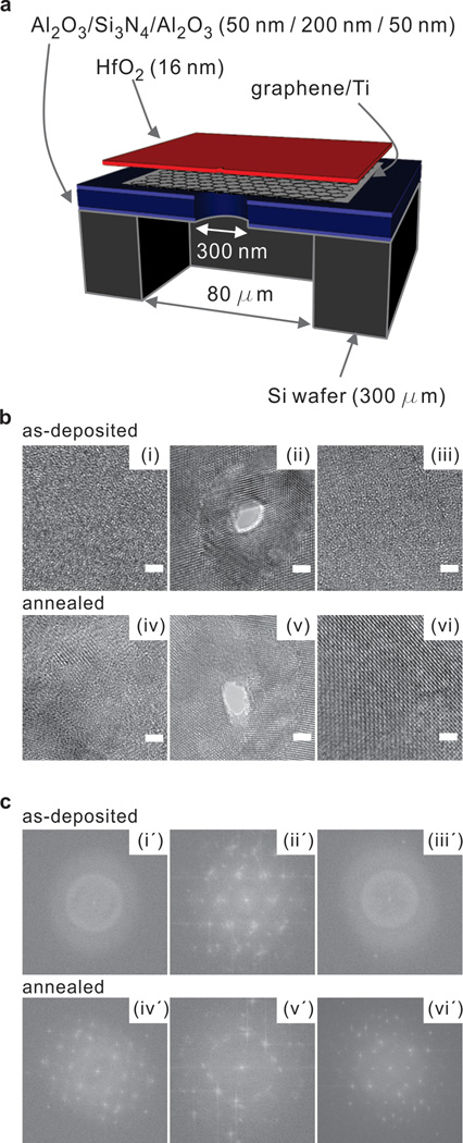
Figure 1. Schematic of membrane fabrication and TEM images with its corresponding FFT images.
a) Schematic cross-section of our membrane architecture. b) TEM phase contrast images of as-deposited amorphous (i~iii) and annealed (iv~vi) HfO2 films deposited on a graphene supported membrane. (i) As-deposited HfO2 membrane before being exposed to a focused electron beam for drilling a nanopore. (ii) A nanopore drilled in amorphous HfO2 film showing electron beam induced crystallinity in the vicinity of the pore. (iii) HfO2 bulk phase which is ~70 nm away from a focused electron beam remains amorphous after a nanopore formation. (iv) Annealed HfO2 membrane before being exposed to a focused electron beam. (v) A nanopore was drilled in annealed HfO2 membrane. (vi) Annealed HfO2 bulk phase which is ~70 nm away from a focused electron beam. (iv~vi) Annealed HfO2 membrane showed crystallinity at all stages. c) FFTs of corresponding TEM image found in Figure 1a confirming amorphous (i’, iii’) and crystallized (ii’, iv’, v’, vi’) phases before and after nanopore formation.

