Abstract
Biosensors are used for the detection of biochemical molecules such as proteins and nucleic acids. Traditional techniques, such as Enzyme-linked Immuno-sorbent Assay (ELISA) are sensitive but require several hours to yield an assay and usually require attaching a fluorophore molecule to the target molecule. Micromachined biosensors that employ electrical detection are now being developed. Here we describe one such device, which is ultrasensitive, real time, label-free and localized. It’s called the nanoneedle biosensor and shows promise to overcome some of the current limitations of biosensors. The key element about this device is a 10nm wide annular gap at the end of the needle, which is the sensitive part of the sensor. The total diameter of the sensor is about 100nm. Any change in the population of molecules in this gap results in a change of impedance across the gap. Single molecule detection should be possible because the sensory part of the sensor is in the range of bio molecules of interest. To increase throughput we can flow the solution containing the target molecules over an array of such structures, each with its own integrated readout circuitry to allow ‘real-time’ detection (i.e. several minutes) of label free molecules without sacrificing sensitivity. To fabricate the arrays we used electron beam lithography together with associated pattern transfer techniques. Preliminary measurements on individual needle structures in water are consistent with the design. Since the proposed sensor has a rigid nano-structure, this technology, once fully developed, could ultimately be used to directly monitor protein quantities within a single living cell, an application that would have significant utility for drug screening and studying various intracellular signaling pathways.
II. INTRODUCTION
Conventional means to detect infectious agents rely on growth cultures. These methods are based on the ability of pathogenic species to multiply in nutrient-rich medium containing selective agents that inhibit the growth of non-target organisms and are particularly useful for differentiating target from non-target organisms. These procedures are sensitive and accurate, but can take as long as several days. More recent techniques such as Polymerase Chain Reaction (PCR) and Enzyme-linked Immunosorbant Assay (ELISA) can directly detect pathogen-specific DNA and proteins, respectively, and can be completed in a matter of hours [1–3]. PCR is extremely sensitive and has been shown to detect as few as 10 or fewer organisms, whereas ELISA, although less sensitive, has the ability to detect proteinaceous toxins that PCR cannot [4–5]. Together, these techniques can provide highly sensitive and specific detection of pathogens and are currently the commonly used techniques in both clinics and research laboratories. While advances in-vitro diagnostics continue to push the limit of sensitivity and specificity, an emerging theme in the field of biosensors has been to make the real-time and multiplex detection of pathogens possible. A multiplex assay is a type of laboratory procedure that simultaneously measures multiple analytes in a single assay and a biomarker is a characteristic that is objectively measured and evaluated as an indicator of normal biologic processes, pathogenic processes, or pharmacologic responses to a therapeutic intervention. Recent development in nanotechnology has further provided the necessary tools for the miniaturization of sensing and transducing elements so that complicated electronic circuits can be integrated into a miniature device that allows real-time, multiplex detection of pathogens from a small sample volume. Biosensors that detect events such as binding of single cells or molecules use either optical (usually fluorescent) or electrical detections. Optical techniques are very sensitive and can detect single molecule events but require the attachment of a fluorophore molecule to the target. Electrical techniques do not require the attachment of fluorophores or other labels but are less sensitive. Optical techniques are more sensitive compared to thermal and electrical techniques because in optical detection, a single or few photons excitement in a process such as photoelectric or avalanche phenomena can be amplified and is sufficient to initiate a detectable flow of electrons (current) [6–8].
Even though the fluorescent platforms usually have higher sensitivity and signal to noise ratio (SNR) compared to the electrical biosensors, the electrical biosensors have the advantages of ease of use, as well as direct, label free and real-time monitoring of events. Impedance biosensors are one class of the electrical biosensors which show promise for point-of-care and some other applications [9–20]. Being low cost, easy to miniaturize, and label-free detection are some advantages of impedance biosensors. Nanopores, electrode-gated system and Semiconductor Nanowire Field Effect Transistors (SiNW) are some types of biosensors that are working based on electrical detection. As of now the best performance for the electrical biosensors is reported for the SiNW Field Effect Transistors [23–26]. They have achieved an SNR ratio of ~3 for the concentration of 90 fg/ml or 2.5 fM for PSA protein while the monoclonal anti-PSA receptor (10–100 µg/ml) is immobilized into a PDMS channel. Here we describe a novel and new nanoneedle biosensor, which shows promise to overcome some of the current limitations of biosensors. Fabrication of the nanoneedles arrays with state-of-the-art nanofabrication techniques allows us to monitor an event instantaneously in a large area, similar to optical detection techniques. The nano-size sensing area of the nanoneedle biosensor results in a high sensitivity detection platform. Furthermore, with the current microfabrication techniques, on-chip amplification of read-out signals from the nanoneedle devices is achievable. Since the proposed sensor has a rigid nano-structure, it can ultimately be used to directly monitor protein quantities in a single living cell, once fully developed.
III. NANONEEDLE BIOSENSOR CONCEPT
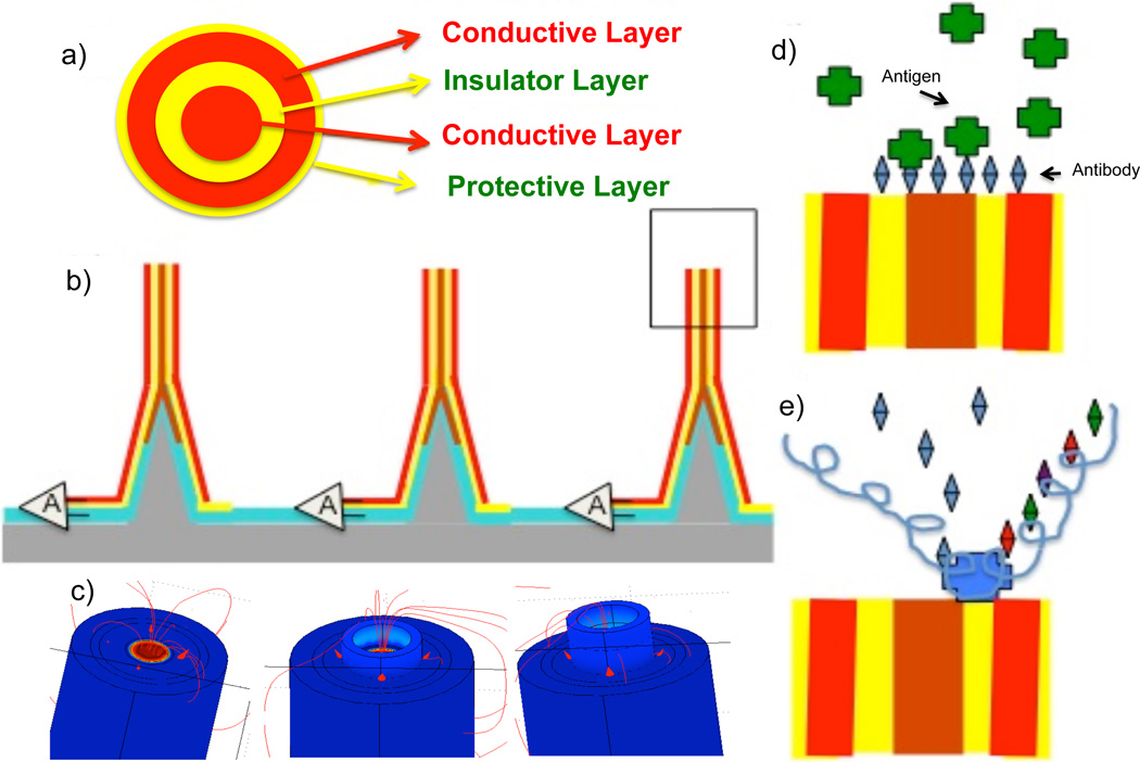
There are two different configurations of nanoneedle biosensors: vertical and horizontal structures. The basic configuration of the vertical nanoneedle consists of four thin-film layers (figure 1). The middle core is made of a metal or a highly doped semiconductor (20 nm diameter). There is an insulator layer (~10nm thick)[21–22], surrounded by another metal layer (~10nm thick), followed by a protective insulator layer. The sensor length can be varied from 350 to 400 nm. The top region of the middle insulator layer is the sensing area of the sensor. This region is in the range of bio-molecules of interest; therefore the binding of just few biomolecules at the sensing area can cause a significant change in impedance.
Figure 1.
Nanoneedle schematic: a) top view of the annular nano-gap; b) array of vertical nanoneedles with on-chip amplification read-out, c) the three different binding Phases: 1) bare needle 2) w/ probe molecule 3) target + probe molecule; d) detection of protein or anti-body-antigen interaction e) DNA sequencing through the impedance modulation (pH/conductance sequencing) detection in direct binding or bead-based systems. Here shown is a polymerase molecule binding to the annular nano-gap area and reading the polymerization binding of different nucleotides. Similarly the assay can be used for a DNA coated bead system with an array of annular nanogaps laid in the channel.
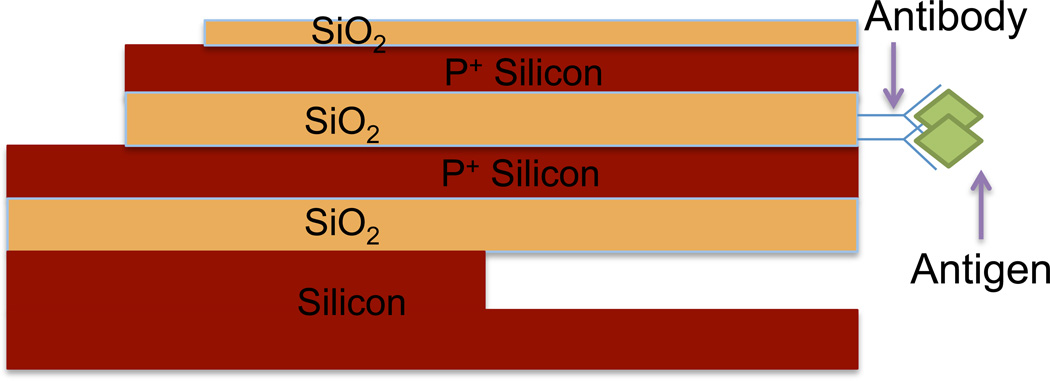
The structure of the horizontal nanoneedle biosensors consists of four thin-film layers (figure 2). There are two conductive layers with an insulator layer in between. An additional oxide layer acts as a protective layer above the sensor. This layer is to prevent the exposure of the conductive electrodes to the solution. Underneath the bottom electrode is another oxide layer, which can be a thermally grown oxide. This layer insulates the first electrode from the substrate. We fabricated and tested various thicknesses and geometrical designs of nanoneedle biosensors. The thickness of the electrodes is 100 nm; and the middle oxide layer thickness is 20 nm. Top protective oxide layer is 30 nm thick and the bottom oxide layer thickness is 250nm. The width of the sensor is 5 µm. The mechanism of operation for both structures is as follow: first the probe molecule is immobilized at the sensor surface and then the target analyte is introduced to the sensor. The probe molecule captures the target analyte, which modulates the impedance at the sensitive part of the sensor.
Figure 2.
Schematic of a horizontal nanoneedle biosensor.
IV. NANONEEDLE BIOSENSOR ADVANTAGES
The detection limit, or the minimum detectable concentration of bio-species in an injected media, is a key figure of merit for biosensors. This depends on the sensitivity (the minimum number of similar binding events to occur to get a detectable signal), flow rate, diffusion time of target molecules, and sensor geometry. This figure of merit is improved in the nanoneedle devices because only a few binding events in the nano-size sensing area of the sensor are enough for impedance modulation in the device. In most practical cases, the system is reaction limited. Since the main concept of high sensitivity array based detection with an annular gap doesn’t require it to be on a shaft, the selection of nanoneedle structure was based on fabrication considerations for application to in-vivo monitoring of events inside of a cell and the three dimensional diffusion.
-
▪
3D vs. 2D diffusion: Most of the current electrical biosensors are planar (two dimensional) and the diffusion phenomena of bio-species take place in two dimensions. Since the nanoneedle devices have a suspended geometry, diffusion takes place in three dimensions in a channel, which results in a higher hit rate of target molecules to the probe molecule per sensor, and thus a faster detection platform.
-
▪
In vivo Monitoring: Most of the current biosensors cannot be mobile over a sample, due to their planer fixed structure. Since the proposed nanoneedle sensor has a rigid nano-structure, a thin functionalized needle can ultimately be used inside of a single living cell to directly monitor protein quantities.
-
▪
Parallel processing: The array processing and multiplexing is an important feature to enable high throughput proteomics and genomics on a large scale. Fabrication of an array of parallel nanoneedle sensors in a microfluidic channel with their individual on-chip amplifier and read out system is a feature that improves the detection limit and speed of detection for this sensor.
-
▪
Impervious to the environment noise in fluidics: The environmental noise due to the perturbation in fluidics has a smaller effect in the nanoneedle structure, especially when real clinical samples (e.g. blood) are used. One figure of merit in biosensors would be how impervious the readout signal is to random motion and movement of the large macromolecule in the solution. Since the sensing area of the sensor is the nano-size region on top of the nanoneedle sensors, the movement of macromolecules in the solution does not affect the device performance.
-
▪
Integrated Handheld Device: On-chip amplification of the electrical signal as well as on-chip microfluidic units can be integrated with arrays of thousands of nanoneedls in microfluidic channels in a single portable device with clinical application for detection of a number of biomarkers in parallel for improved early stage diagnoses.
V. SIMULATION RESULTS
Vertical Nanoneedle Biosensor
The most important issues in biosensor development for the past several decades have been the sensitivity and the selectivity of the detector. Most of the devices usually suffer from small SNR due to different sources of noise (e.g. electrical, thermal, Flicker, Johnson, etc.) and low signal detection (e.g. the signal generated due to a reaction or binding event of a target molecule to the probe molecule is not large enough). Especially compared to most optical techniques, electrical biosensors have suffered from lack of high sensitivity, which is very critical in early stage diagnosis. Study of impedance modulation in the nanoneedle was used to study the operation of the device. We studied several capacitances and resistances within the device and their dependence on geometry. Figure 3a shows the impedance modulation results of the device by using FEM modeling (COMSOL) and double layer capacitance calculation (e.g. 0.20 uF/mm2).
Figure 3.
a) Finite element modeling (COMSOL) of impedance modulation of a nanoneedle and a double layer capacitance calculation for a core needle ~30nm diameter, insulator layer ~20nm, second conducting layer ~7nm and outside insulator protective layer ~15nm. b) FEM COMSOL modeling of a vertical nanoneedle with an applied electric potential.
COMSOL simulation was a static analysis in 3D space dimensions. Mesh setting was as below. Sequence type was physics-controlled mesh with the fine element size. Number of vertex elements was 133; number of edge elements was 1283, number of boundary elements was 8943, free meshing time was 3.50s and minimum element quality was 0.2397. For the computation of the model by using linear geometry shape order for the mesh element near the coordinates and the linear solver, solution time was 26 s. Number of degrees of freedom solved for 79624. Object type for all the layers defined as solids. For this simulation, the diameter of core needle was set to 30nm and the material was defined as a gold (Au) layer with the electrical conductivity of 45.6*106 [S/m]. The boundary initial voltage for the inner core was set to 100 mV. For the all other boundaries, the boundary settings were set to Electrical Shielding, Continuities or Ground, depending on their relevance. An insulator layer was defined around the core needle as a 30 nm thick SiO2 with the relative permittivity of 4.2. Another gold layer with the thickness of 7nm was defined as the second conductive layer with the same electrical conductivity as the core needle. This layer was surrounded by a defined 15 nm SiO2 protective layer. The length of needle was set to 250 nm. To obtain the bode plot; the needle was simulated at different frequencies. First, the bare needle was simulated. Then a hollow ring was placed on the sensor surface to simulate the immobilization of the probe biomolecules. The impedance response of the sensor was distinguished. Then another ring was defined and placed on top of the “probe bio molecules” to simulate a target binding and the new impedance response was distinguished. For the impedance simulation the time harmonic Electrical Currents application mode within the AC/DC Module was used. To allow the COMSOL to generate an impedance value for the nanoneedle, the boundary settings of the core needle were set to Port using a Fixed Current Density and the top of the needle was set as the input port. The scalar frequency variable associated with the Electric Currents application mode was changed with each simulation to obtain the impedance at different frequencies.
The change of impedance for different concentrations of ionic solutions, which corresponds to the ionic solution resistance and the change during binding of the bio-species to the needle, was also simulated. For the shown simulation results in figure 3, 20% of the sensor surface was covered with the proteins, which were defined in boxes of 5×5×20 nm. Based on the simulation results, the binding of protein molecules to the sensor surface resulted in 92µV signal generation (with 20% coverage). Total noise (e.g. thermal, ADC and amplifier noise) is about 6 µV rms, which results in a SNR = 15/per protein molecule. In order to have SNR ~ 3 as reported for the SiNW Field Effect Transistors [23–26], theoretically only 4% coverage of the sensors surface by proteins is required to generate such a signal. As a result, binding of only 15 proteins (defined in boxes of 5×5×20 nm) is theoretically enough to have such an SNR.
Horizontal Nanoneedle Biosensor
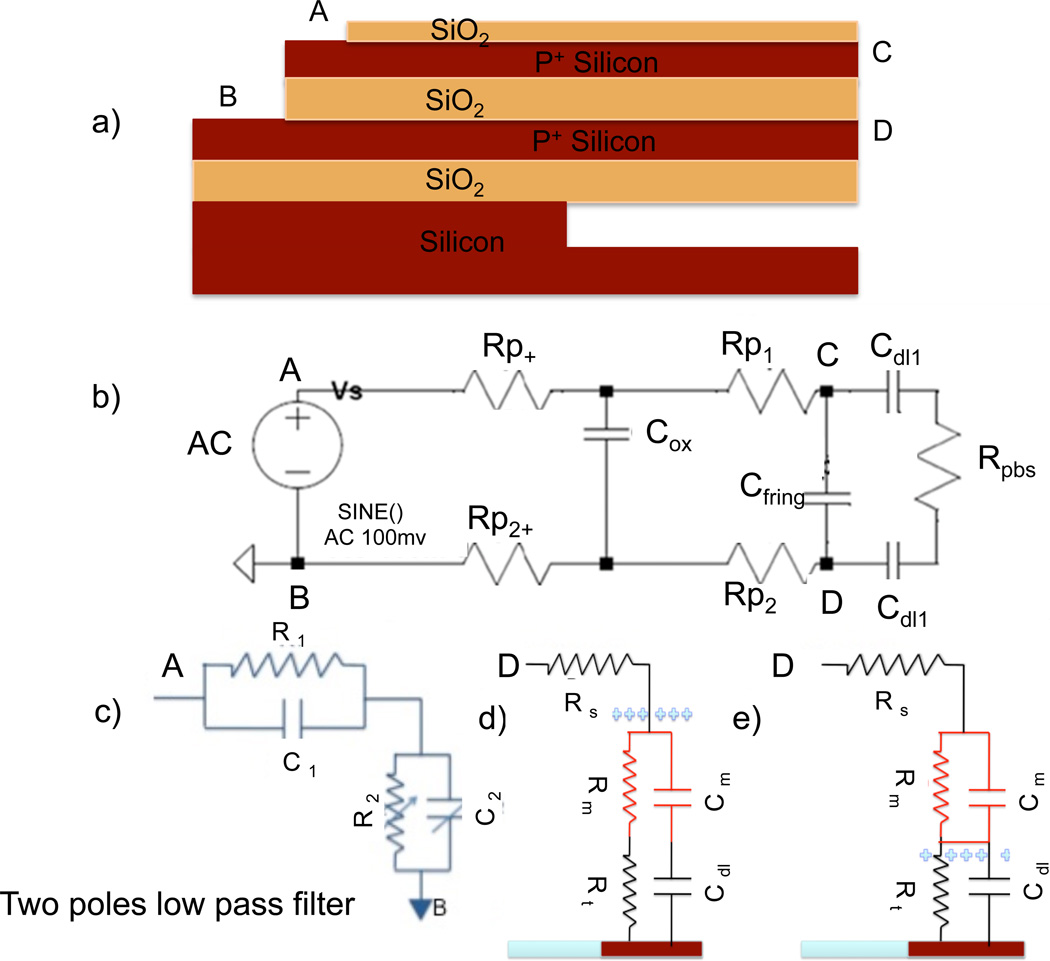
The electrical modeling of the horizontal nanoneedle biosensor is shown in figure 4. The schematic illustration of the fabricated horizontal nanoneedle is shown in figure 4a and the electrical modeling of the device is shown in figure 4b. The resistances of conductive layers are shown as Rpx. Cox and Cfirg correspond to the bulk layer capacitance and fringing capacitance respectively. The sensitive part of the sensor (middle oxide layer) experiences a double layer capacitance (Cdl) at the electrode interfaces with the ionic solution. Double layer capacitance depends on the ionic concentration and conductive surface area [e.g. 0.20 µF/mm2 for PBS 50mM]. Rpbs is representing the ionic resistance of the solution, which varies with the type and concentration of ionic solutions, bio-molecules concentration, geometry and the thickness of middle oxide layer.
Figure 4.
Electrical circuit model for a naoneedle biosensor. a) Schematic of a horizontal nanonneedle sensor b) Electrical modeling corresponding to the top device, b) Equivalent two-pole low pass filter; c) Electrical modeling of top of nanoneedle with bio-molecule bound to the sensor surface and in close approximately to the surface, d) Model when the molecule is in the double layer region and e) when the molecule is outside of the doublelayer region (3–10 nm).
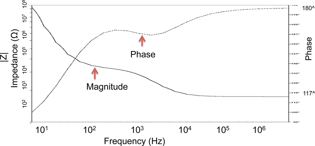
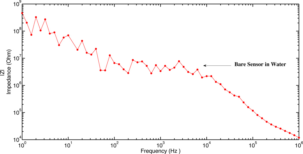
Two steps of operation for the nanoneedle biosensors are the loading step and detection step. In the loading step, the probe bio-molecule binds to the nanoneedle tips. The capturing and binding of the target bio-molecule with the probe molecule is called the detection step. Two possible scenarios depending on the size of bio-molecules and ionic concentration are shown in figure 4c and figure 4d. As it’s shown in figure 4c, a small molecule binds to the surface of the nanoneedle and sits in the double-layer area. The modulation in the impedance and the detection scheme is dependent on the relocation of the ions shielding the surface of the electrode (Cdl). The other possibility, which is more common in the practical biosensing applications, is that the molecule binding occurs outside of the 3–10nm shielded layer from the needle’s surface (figure 4d). In this case the detection is based on the impedance modulation due to the addenda molecule’s RC model, while the biomolecule binds to either the surface of the needle (loading phase) or the probe biomolecule (detection phase). In both cases, in addition to the change of double-layer capacitance, the ionic resistance of the solution may change due to a change of local ionic concentration around the needle’s surface while the charged biomolecules are present. Therefore the depletion or accumulation of cation or anion concentration changes the Rpbs. The proposed electrical model of the device was simulated with the circuit design simulator, TSPICE. Simulation results of impulse response for this structure are shown in figure 5. These simulation results were confirmed with the impulse response of the fabricated and characterized sensor (figure 13a), which will be explained in details in the sensor characterization section.
Figure 5.
Simulation modeling with T-Spice for impedance vs. frequency for the modified device.
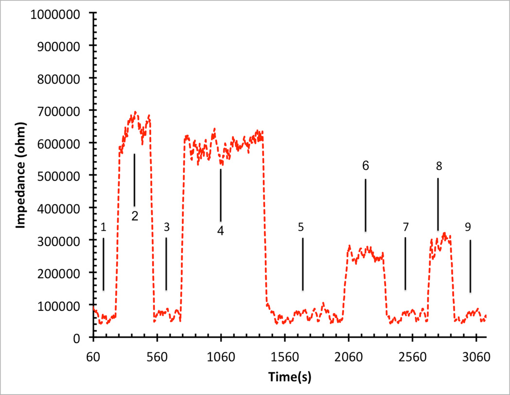
Figure 13.
a: Experimental result of impulse response for a fabricated horizontal nanoneedle biosensor
b: Impedance versus time for horizontal nanonnedle assay with the test solutions when 10X PBS, water, 10X PBS, water, 10X PBS, 1X PBS, 10X PBS, 1X PBS and 10X PBS was injected to the channel in steps 1,2,3,4,5,6,7,8 and 9 respectively.
VI. FABRICATION APPROACHES
Below we describe the fabrication process details for both vertical and horizontal nanoneedle biosensors.
Horizontal Nanoneedle Array Fabrication
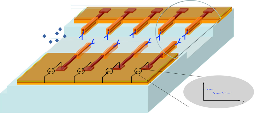
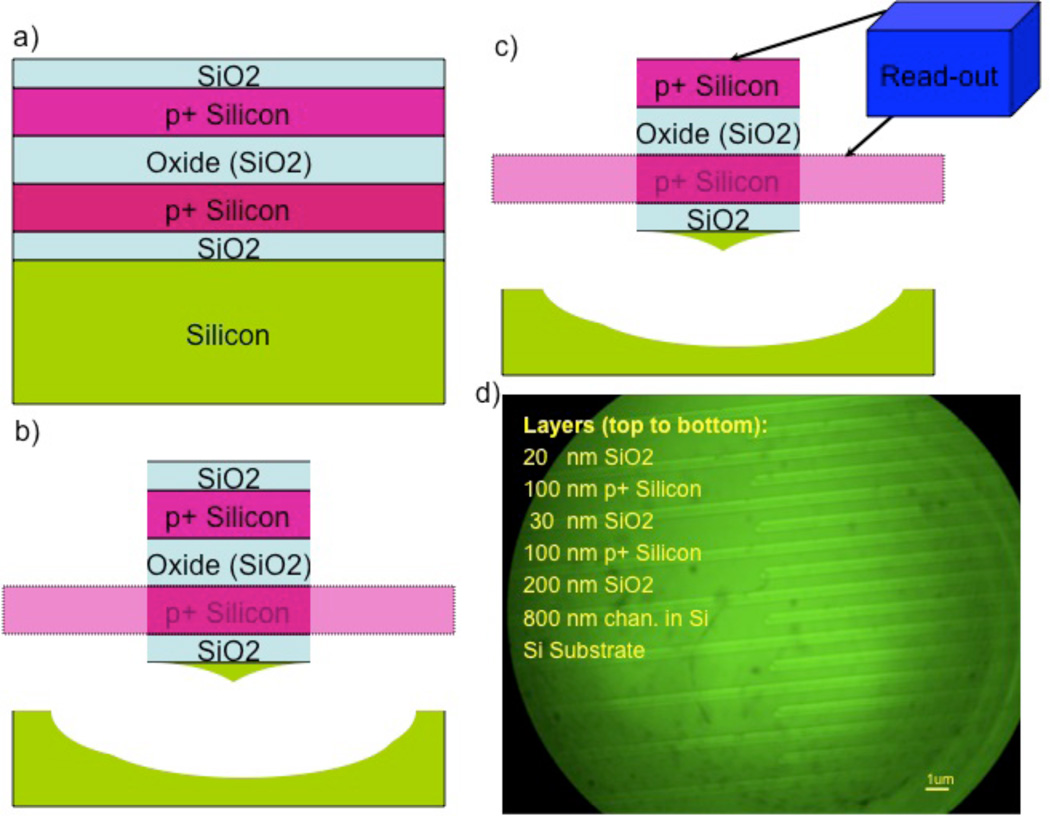
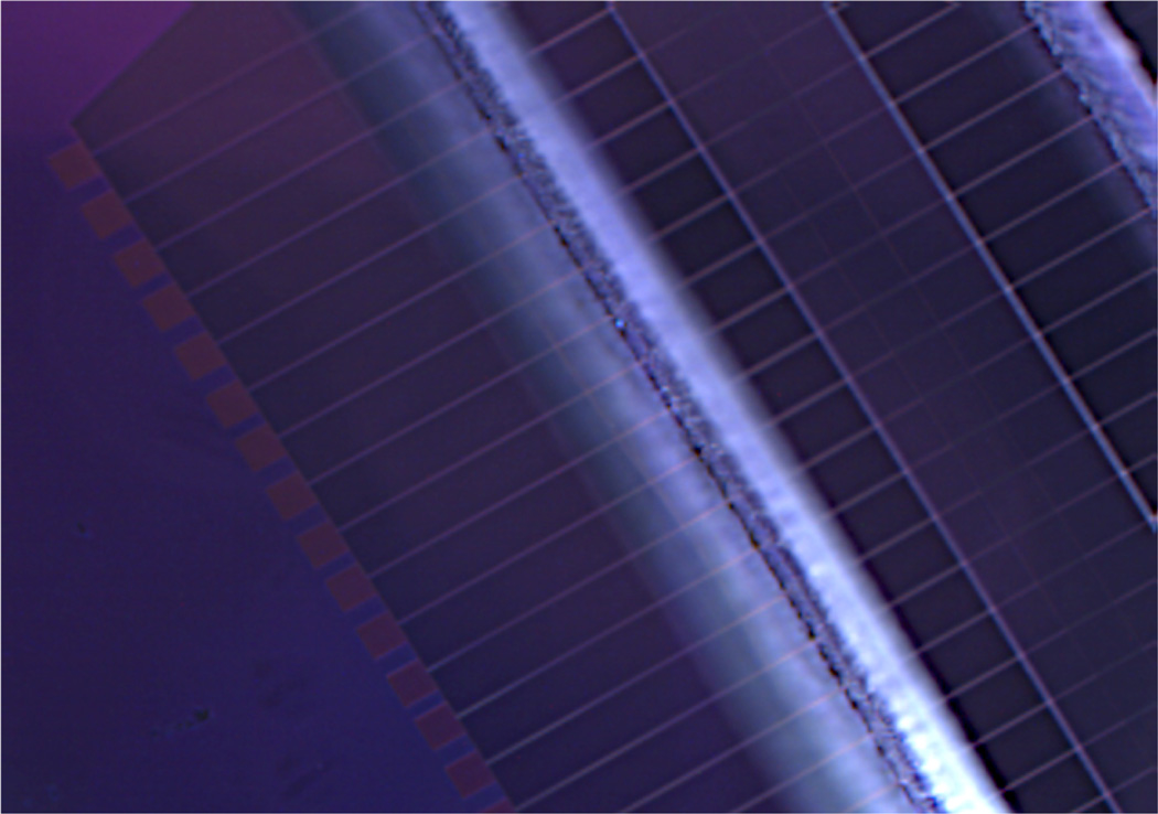
600 individual nanoneedle devices in 15 bundles of 40 nanoneedle sensors per bundle were fabricated on a 4 inch silicon wafer. A schematic of the nanoneedle biosensor array is shown in figure 6. The fabrication process of these devices was designed for a minimum number of steps. First, 250nm of silicon dioxide was thermally grown on a silicon substrate to insulate the first electrode from the substrate. This was followed by low-pressure vapor deposition (LPCVD) of a 100 nm thick poly-silicon layer, which forms the bottom electrode. This electrode was then doped with phosphorus to achieve a sheet resistance of 210 ohm per square. This p+-silicon layer was then coated with a 30nm thick SiO2 layer deposited by the Plasma Enhanced CVD (PECVD) technique. This was followed by another LPCVD p+-silicon layer deposition to form the second electrode followed by a phosphorus doping to achieve the same conductivity as the bottom electrode. Finally a 20 nm PECVD protective SiO2 layer covers the top electrode. This is followed by three lithography and etching processes. First, 1.6 um SHIPLEY 3612 resist was spin-coated (SVG coat), exposed (Karlsuss), baked for 120 sec, and developed (SGV Develop). Then 20nm top-SiO2, 100nm top p+-silicon, and 30nm middle oxide layer were etched down to bottom p+-silicon layer by dry-etching (P5000). After a second lithography process, the remaining 100nm bottom p+-silicon and 200nm bottom SiO2 were etched as well as 1µm into the Si substrate to produce a structure similar to the first layer (figure 7c), except for the electrical pad sections. This was followed by XeF2 dry etch to open the channel underneath the nanoneedle devices. Finally the silicon dioxide was removed from the electrical pad areas to enable access to the contacts for measurements. The schematic of this fabrication process is shown in figures 8a and 8b. In figure 8d, a micrograph of the nanoneedle array in an interdigitate structure is shown. Finally, a premade PDMS micro-channel was thermally bonded on top of the nanoneedle devices. These channels have dimensions of 100µm height, 800µm width and 7.1 mm length located on top of each bundle, while the pad areas are cut and opened for measurement access. Optical micrograph of a fabricated array of horizontal nanoneedles sensors with a PDMS channel on top is shown is figure 9 (bird’s eye view). To optimize the sensor functionality, different thickness of conductive and insulative layers, single, multiple and interdigit structures were fabricated and tested (figure 10).
Figure 6.
Schematic illustration of horizontal nanoneedle array in a microfludic channel. There is an etched silicon channel underneath the parallel nanoneedles and PDMS microfluidic on top of the array. The needles are individually accessible for testing thought the electrical contact pads. The impedance of the nanoneedls is modulated with the attachment of biomolecules.
Figure 7.
SEM image of a) post-exposure and b) post development of SPL study, horizontal nanoneedle structure, 2% 950K MW PMMA-Anisole, d= 102 nm, c) Details of the horizontal nanoneedle structure (top-view), d) the SPL with 8.93nm width post-development, large LER, Image courtesy: J. W. Conway, Stanford Nanofabrication Facility.
Figure 8.
a & b) Schematic of the fabrication process for horizontal nanoeedle array; c) Measurement phase, d) Micrograph of an interdigitated nanoneedle array..
Figure 9.
Optical micrograph of a fabricated array of horizontal nanoneedle sensor from a bird’s eye view. A PDMS channel is located on top of the sensors.
Figure 10.
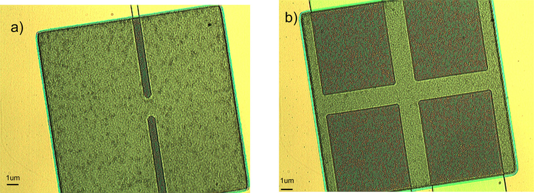
Micrographs of single and double nanoneedle biosensors from a bird’s eye view.
Vertical Nanoneedle Fabrication
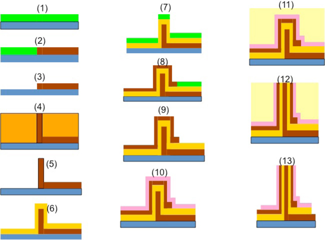
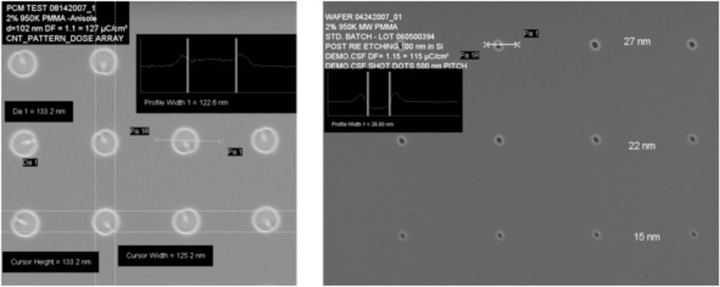
Fabrication of vertical nanoneedle devices includes the fabrication of its core needle, the middle insulator layer and the second conductive layer, which is surrounded by a protective insulative layer. The fabrication process is as follow: Electron-beam Lithography Method: One of the most robust techniques to generate reproducible arrays of nanoneedles is through a combination of electron beam lithography and etching. The schematic of the fabrication process for the array of standing naoneedle sensors with e-beam patterning is shown in figure 11. The patterns for the nanometer-scale structures were fabricated by electron-beam lithography (EBL) using a Raith150 system (Raith GmbH, Dortmund, Germany). After wafer cleaning, the silicon substrates were coated with 100 nm thick 2% 950K Poly Methyl Methacrylate positive electron beam resist (Microchem Corp) and soft baked for 120 s at 200 °C. The resist was then exposed to an electron beam at an acceleration voltage of 10 kV using an electron dose of 100 µC/cm2 to pattern all the area. The beam current measured 0.186 nA. After EBL exposure, the resist was developed by soaking in a methyl isobutyl ketone/ isopropyl alcohol (MIBK/IPA) 1:3 by volume solution for 30 s at 18 °C, and then rinsed with pure 2-propanol for 30 seconds. After lithography, the samples were reactively ion etched (RIE) in an Applied Materials P-5000 MERIE system in a two-step RIE process. The initial etching step removed the intrinsic native silicon dioxide layer over the silicon substrate using CF4 for 5 s (100 mT, 250 W), followed by RIE of the silicon substrate using a 1:1 ratio of Cl2 to HBr for 1 min (100 mT, 250 W 40 G magnetic field). The ZEP-520 thin film was stripped using Piranha etchant (9:1 H2SO4/H2O2, 120 °C). Figure 12 shows the post exposure of the dot array (left) and the post development (right) of the cylindrical holes ion 100nm PMMA resist. The sizes of holes range from 8 to 150 nm in diameter. It was followed by the metal sputtering deposition of Au and lift-off process for the core (right) electrode fabrication, which is shown in steps 1 to 5 in the figure 11. In step (6), the oxide layer (30 nm of SiO2) is deposited on top of the metal (Au) layer. The fabrication of the second electrode (left one in the figure 11) in step 7 to 9 is followed by the deposition of a protective oxide layer (step 10). Then by using CMP (Chemical Mechanical Polishing), the needles tips are opened for functionalization by probe bio-molecules. This process is shown in steps 11 to 13.
Figure 11.
Schematic of the process flow for the fabrication of vertical nanoneedle.
Figure 12.
SEM images of post-exposure (left) and post development (right) of dot array fabrication of vertical nanoneedle structure, 2% 950K MW PMMA-Anisole, d= 102 nm, left: DF= 1.1 = 127 uC.cm2, Right: DF = 0.1 = 0.01 pAsec, Mag = 50,000×, Image courtesy: J. W. Conway, Stanford Nanofabrication Facility.
VII. SENSOR CHARACTERIZATION
In order to electrically characterize horizontal nanoneedle biosensors, the impedance versus frequency of the fabricated sensor in water was measured. The impulse response of the fabricated horizontal nanoneedle biosensor is shown in figure 13a. This experimental measurement follows the same trend as the simulation results, which confirms the modeling results (shown in figure 3a). The difference in magnitude of measured impedance could be due to the difference in solutions salt concentration, conductivity of the electrodes, and not perfectly fabricated sensors compared to what we used for the simulations. As a preliminary study, the impedance of the devices for 10× Phosphate Buffered Saline (PBS), 1× Phosphate Buffered Saline and water were measured and the results are shown in figure 13b. A sinusoidal voltage signal with 100mV RMS (at 10 KHz) was applied to the top polysilicon electrode and the entering current to the bottom electrode was measured by using a Versa STAT3 potentiostat. The ratio of the applied voltage to the passing current gives the value of the measured impedance. 1X Phosphate Buffered Saline solution (PBS) is a water-based salt solution containing 800ml-distilled H2O, 8g of NaCl, 0.2g of KCl, 1.44g of Na2HPO4 and 0.24g of KH2PO4 and its pH is adjusted to 7.4. 10X PBS containins 800ml distilled H2O, 80g of NaCl, 2.0g of KCl, 14.4g of Na2HPO4 and 2.4g of KH2PO4 (pH 7.4). To test the functionality of the sensors, 10X PBS, water, 10X PBS, water, 10X PBS, 1X PBS, 10X PBS, 1X PBS and 10X PBS were injected into the channel in steps 1,2,3,4,5,6,7,8 and 9 respectively. Each solution was injected into the channel in different steps and the experiment was performed several times to test repeatability of the results. It was a real time measurement with continues flow of each buffer to the channel. From impedance vs. time measurements at various ionic concentrations, a significant difference between deionized (DI) water and different concentration of PBS was observed which is due to the change of buffer conductivity due to the presence of free ions in the PBS buffer (which affects Rpbs) and the difference of their relative dielectric permittivity (which affects the Cfirg and Cdl).
VIII. CONCLUSIONS
Two different nanoneedle device structures were proposed as integrated, localized and real time sensors to detect biological molecules in low concentrations. The impedance modulation at the nano-size tip of the sensors with the change in the population of bio-molecules at the sensing area of the sensor results in a high sensitivity detection platform. The proposed nanoneedle devices can be fabricated in an array of thousands for high throughput genomics or proteomics studies. Since the proposed sensor has a rigid nanostructure, this technology once fully developed, could ultimately be used to directly monitor protein quantities within a single living cell, an application that would have significant utility for drug screening and studying various intracellular signaling pathways. The primary devices were fabricated and the details of the fabrication process for both vertical and horizontal structures of the sensors were explained. The finite element modeling and electrical circuit modeling of the system were discussed. As the preliminary study, fabricated horizontal sensors were electrically characterized by using different concentration of Phosphate Buffered Saline solutions and water. Experimental measurements confirmed functionality of the sensors and accuracy of the simulation results.
ACKNOWLEDGMENTS
The authors like to thank J.W. Conway from Stanford Nanofabrication Facility for the SEM Images and Asad Kalantarian for his useful comments and discussions. The fabrication of this works was done in Stanford Nanofabrication Facility and Stanford Microfluidic Foundry. This work was supported under NIH grant No. PO1HG000205.
References
- 1.John Butlera E. Enzyme-Linked Immunosorbent Assay. Journal of Immunoassay. 2000;Volume 21(Issue 2–3):165–209. doi: 10.1080/01971520009349533. [DOI] [PubMed] [Google Scholar]
- 2.ENZYME-LINKED IMMUNOSORBENT ASSAY, ELISA Quantitation of Specific Antibodies by Enzyme-Labeled Anti-Immunoglobulin in Antigen-Coated Tubes. EVA ENGVALL et al. ; JOURNAL OF IMMUNOLOGY. 1972;Vol. 109(No. 1) [PubMed] [Google Scholar]
- 3.Clark Michael F, Adams AN. Characteristics of the microplate method of enzyme-linked immunosorbent assay for the detection of plant viruses. Journal of general virology. 1977;34.3:475–483. doi: 10.1099/0022-1317-34-3-475. [DOI] [PubMed] [Google Scholar]
- 4.Bell CA, Uhl JR, Hadfield TL, et al. Detection of Bacillus anthracis DNA by LightCycler PCR. J Clin Microbiol. 2002;40:2897–2902. doi: 10.1128/JCM.40.8.2897-2902.2002. [DOI] [PMC free article] [PubMed] [Google Scholar]
- 5.Andreotti PE, Ludwig GV, Peruski AH, Tuite JJ, Korse SS, Peruski LF., Jr Immunoassay of infectious agents. BioTechniques”, 35:850-9. Clin. Pharmacol Ther. 2003;69:89–95. doi: 10.2144/03354ss02. 2001. [DOI] [PubMed] [Google Scholar]
- 6.Haes Amanda J, Van Duyne Richard P. A nanoscale optical biosensor: sensitivity and selectivity of an approach based on the localized surface plasmon resonance spectroscopy of triangular silver nanoparticles. Journal of the American Chemical Society. 2002;124.35:10596–10604. doi: 10.1021/ja020393x. [DOI] [PubMed] [Google Scholar]
- 7.Cush R, et al. The resonant mirror: a novel optical biosensor for direct sensing of biomolecular interactions Part I: Principle of operation and associated instrumentation. Biosensors and Bioelectronics. 1993;8.7:347–354. [Google Scholar]
- 8.Haes Amanda J, et al. Detection of a biomarker for Alzheimer's disease from synthetic and clinical samples using a nanoscale optical biosensor. Journal of the American Chemical Society. 2005;127.7:2264–2271. doi: 10.1021/ja044087q. [DOI] [PubMed] [Google Scholar]
- 9.Basuray S, Senapati S, Aijian A, Mahon AR, Chang HC. ACS Nano. 2009;3:1823. doi: 10.1021/nn9004632. [DOI] [PubMed] [Google Scholar]
- 10.Daniels JS, Pourmand N. Electroanalysis. 2007;19:1239. doi: 10.1002/elan.200603855. [DOI] [PMC free article] [PubMed] [Google Scholar]; [24] Ge bala M, Schuhmann W. ChemPhysChem. 2010;11(13) doi: 10.1002/cphc.201000210. [DOI] [PubMed] [Google Scholar]
- 11.Bonanni A, Fernández-Cuesta I, Borrisé X, Pérez-Murano F, Alegret S, Valle M. Mikrochimica Acta. 2010;170(275) [Google Scholar]
- 12.Zhang G, Zhu R. Electroanalysis. 2010;22(3) [Google Scholar]
- 13.Kendall JKR, Johnson BRG, Symonds PH, Imperato G, Bushby RJ, Gwyer JD, van Berkel C, Evans SD, Jeuken LJC. ChemPhysChem. 2010;11(10) doi: 10.1002/cphc.200900917. [DOI] [PubMed] [Google Scholar]
- 14.Chen X, Guo Z, Yang G-M, Li J, Li M-Q, Liu J-H, Huang X-J. Materials Today. 2010;13(28) [Google Scholar]
- 15.Ignat T, Miu M, Kleps I, Bragaru A, Simion M, Danila M. Materials Science and Engineering B. 2010;169(55) [Google Scholar]
- 16.Rajesh V Sharma, Tanwar VK, Mishra SK, Biradar AM. Thin Solid Films. 2010;519:1167. [Google Scholar]
- 17.Chang B-Y, Park S-M. Electrochemical Impedance Spectroscopy. Annual Review of Analytical Chemistry. 2010;3(207) doi: 10.1146/annurev.anchem.012809.102211. [DOI] [PubMed] [Google Scholar]
- 18.Lindholm-Sethson B, Nyström J, Malmsten M, Ringstad L, Nelson A, Geladi P. Analytical and Bioanalytical Chemistry. 2010;398:2341. doi: 10.1007/s00216-010-4027-7. [DOI] [PubMed] [Google Scholar]
- 19.Cunningham S, Gerlach JQ, Kane M, Joshi L. The Analyst. 2010;135:2471. doi: 10.1039/c0an00276c. [DOI] [PubMed] [Google Scholar]; [34] Su B, Tang J, Huang J, Yang H, Qiu B, Chen G, Tang D. Electroanalysis. 2010;22(22) [Google Scholar]
- 20.Su B, Tang J, Huang J, Yang H, Qiu B, Chen G, Tang D. Electroanalysis. 2010;22(22) [Google Scholar]
- 21.Esfandyarpour Rahim, et al. MRS Proceedings. Vol. 1572. Cambridge University Press; 2013. Thin Film Nanoelectronic Probe for Protein Detection. [Google Scholar]
- 22.Esfandyarpour Rahim, et al. MRS Proceedings. Vol. 1414. Cambridge University Press; 2012. Electrical Detection of Protein Biomarkers Using Nanoneedle Biosensors. [Google Scholar]
- 23.Patolsky F, Timko BP, Zheng G, Lieber CM. Nanowire-based nanoelectronic devices in the life sciences. MRS Bulletin-Materials Research Society. 2007;vol. 32(no. 2):142–149. [Google Scholar]
- 24.Patolsky F, et al. Electrical detection of single viruses. Proc Natl Acad Sci U S A. 2004;101:14017–14022. doi: 10.1073/pnas.0406159101. [DOI] [PMC free article] [PubMed] [Google Scholar]
- 25.Zheng G, et al. Multiplexed electrical detection of cancer markers with nanowire sensor arrays. Nat Biotechnol. 2007;23:1294–1301. doi: 10.1038/nbt1138. [DOI] [PubMed] [Google Scholar]
- 26.Yazdanpanah M, Harfenist S, Safir A, Cohn RW. Selective self-assembly at room temperature of individual freestanding Ag2Ga alloy nanoneedles. J. Appl. Phys. 2005;98:0735. J. Appl. Phys. 98, 073510. [Google Scholar]


