Abstract
We report here a successful demonstration of a flip-chip packaging approach for a microelectromechanical systems (MEMS) device with in-plane movable microelectrodes implanted in a rodent brain. The flip-chip processes were carried out using a custom-made apparatus that was capable of the following: 1) creating Ag epoxy microbumps for first-level interconnect; 2) aligning the die and the glass substrate; and 3) creating non-hermetic encapsulation (NHE). The completed flip-chip package had an assembled weight of only 0.5 g significantly less than the previously designed wire-bonded package of 4.5 g. The resistance of the Ag bumps was found to be negligible. The MEMS micro-electrodes were successfully tested for its mechanical movement with microactuators generating forces of 450 μN with a displacement resolution of 8.8 μm/step. An NHE on the front edge of the package was created by patterns of hydrophobic silicone microstructures to prevent contamination from cerebrospinal fluid while simultaneously allowing the microelectrodes to move in and out of the package boundary. The breakdown pressure of the NHE was found to be 80 cm of water, which is significantly (4.5–11 times) larger than normal human intracranial pressures. Bench top tests and in vivo tests of the MEMS flip-chip packages for up to 75 days showed reliable NHE for potential long-term implantation.
Index Terms: Actuators, biomedical microelectromechanical systems (MEMS) (bio-MEMS), flip chip, hydrophobic silicone, microactuators
I. Introduction
Packaging has been a significant challenge in the development of cost-effective microelectromechanical systems (MEMS) devices. Often, packaging issues and processes do not get sufficient attention until the MEMS front-end processes have been completely developed. MEMS packaging costs now typically contribute more than 50% [1]–[6] of the total material/assembly cost. The reasons for the higher packaging cost are partly because MEMS devices typically involve active mechanical structures, requiring stringent packaging constraints [7] and different kinds of unconventional sealing techniques, such as nonhermetic [for pressure sensors and biomedical MEMS (bio-MEMS)] and hermetic (for RF MEMS).
MEMS packaging is still mostly done with wire-bonding technique. However, one of the challenges with this technique is to protect the MEMS mechanical structures throughout the packaging process [6], [8]. Unlike ICs, which have no active mechanical structures and are protected by several barrier layers in the back end of the silicon, MEMS dies have no protective layers on top of their active structures. Once MEMS dies are released from the foundry, MEMS active structures are exposed to the ambient. In the past, several groups have used an encapsulation Si cap [9]–[11] on top of MEMS active structures in the wafer level. This encapsulation cap is usually made from a silicon die etched by a Bosch process [7] to create a cavity that subsequently enclosed the MEMS active structure. This technique enables a MEMS die to be handled like an integrated circuit (IC) chip for further packaging steps [12], such as wafer dicing, die attach, and wire bonding. This capping approach has been commercially used by Analog Devices, Inc., for its products such as monolithic accelerometer MEMS/ASIC ADXL330 [13]. Since wire bonding is used, the overall package size is significantly larger than the die size. Panchawagh et al. [14] introduced a flip-chip encapsulation method for the packaging of MEMS actuators by using surface-micromachined polysil-icon caps in combination with wire bonding. Faheem et al. reported a nonhermetic packaging technique for RF MEMS as an alternative way to reduce MEMS packaging costs [15].
The second challenge in connecting the die and the substrate via flip-chip technique is the first-level interconnects (FLIs). Ideally, such flip-chip processes must not interfere with the active MEMS structures. In the past, thermosonic bonding [16] technique has been used to bond Au stud bumps with the substrate. However, such bonding technique may interfere with highly sensitive MEMS microsensors such as microphone membrane. To mitigate this issue, the bonding bump can be located hundreds of micrometers away from the MEMS active area. Pai and Walsh have used anisotropic conductive film (ACF) to bond Au bumps on the substrate [17]. One challenge with this technique is that the ACF particulates may contaminate the MEMS active area when it is applied to the die. This problem has been mitigated by covering the MEMS active area with encapsulation such as a MEMS cap [8], [18]–[21]. Campabadal et al. flip chipped solder bumps on the die with the Au pads on the substrate [22], and in order to avoid any possible flux contamination, the bond pads were placed along the perimeter of the die, providing clearance on the order of several hundreds of micrometers from the MEMS active pads. This technique of moving the bond pads several hundred micrometers away from the MEMS structures therefore increased the MEMS die size and hence enlarged the package size. Most reported MEMS packaging steps via flip chip also require additional microfabrication steps (such as lithography) to develop its FLIs, which electrically connects the die to the substrate. In our previous report [23], we had demonstrated novel Ag microbumps for FLI structures without any visible contamination of MEMS structures and functional impediment of MEMS operation which required no additional microfabrication process. In this paper, we use the aforementioned technique as the building platform for developing a unique flip-chip-based approach for MEMS packaging that solves the aforementioned challenges.
In addition to addressing the challenges involved in flip-chip packaging of MEMS devices in general, this study also addresses specific packaging challenges involved in the successful development of implantable MEMS devices. In some of these applications, microelectrodes extend off the edge of the die and are implanted in brain tissue, making hermetic encapsulation nonviable. Furthermore, MEMS sensors and/or actuators are exposed to biological environments where NHE technology is a critical packaging need for successful operation [24]. This NHE allows the MEMS sensory part (such as a microelectrode) to be exposed to the biological environment while simultaneously preventing body fluids such as cerebrospinal fluid (CSF) and blood, which contain ions and other biological particles, to enter and contaminate the MEMS active structures. Recent reports have demonstrated the use of flip-chip technique to protect the MEMS active structures and seal the MEMS die nonhermetically. Erismis et al. [25] flip chipped a cap (made of a microfabricated silicon or glass substrate) on the MEMS active electrostatic actuators [26] while leaving a small clearance to let the actuator shuttle extend off the device. A hydrophobic coating was used on the surfaces of the clearance. Dy and Ho [27] also demonstrated a NHE technique for a MEMS device used as a cytomic force transducer for a mechanobiology experiment. The electrical interconnects in both of the aforementioned cases were done through wire bonding.
Generally speaking, flip chip is a preferred packaging method for MEMS (including those for implantable applications) as it reduces the overall package size and provides opportunities to scale the number of MEMS chips through multichip package (MCP) or 3-D stacks (hybrid integration through 3-D). In this paper, we report a novel MEMS packaging process that uses flip-chip technique for the following: 1) electrically connecting the MEMS die to the substrate; 2) protecting the MEMS active area with the MEMS chip itself (without the need for external caps such as MEMS cap or package encapsulation); and 3) providing the clearance necessary to create NHE through patterned microstructures of silicone on one side of the package. The finished MEMS package has no exposed traces or wire and hence requires no additional package encapsulation typically used after wire bonding. The reported MEMS packaging steps were used for MEMS movable microelectrodes which had independently actuated microelectrodes protruding outside the MEMS die. The packaged MEMS device was subsequently implanted and tested in long-term in vivo experiments in rodent brains. To the best of our knowledge, this is the first time that flip-chip-bonded devices containing complex MEMS movable microstructures have been successfully tested on the brain.
II. Methods
A. MEMS Testing Samples
There are three different types of MEMS testing samples that have been used in this study for the development of flip-chip packaging technology: 1) folded beam (chevron) type of actuator; 2) linear actuator; and 3) linear actuator with a rotating gear. Chevron actuator mechanism, as shown in Fig. 1, has the smallest feature size of about 1.5 μm and has the most complex actuation mechanism that finally moves the microelectrode with the size of 50-μm width and 4-μm thickness. Therefore, the results from chevron actuator are reported and discussed more frequently in the study. As the flip-chip technology reported in this paper has been tested successfully in three different complex actuator mechanisms (as shown in Fig. 5), we expect the flip-chip method reported here to be applicable for other MEMS designs.
Fig. 1.

Design layout of the MEMS microactuators and microelectrodes on chip.
Fig. 5.
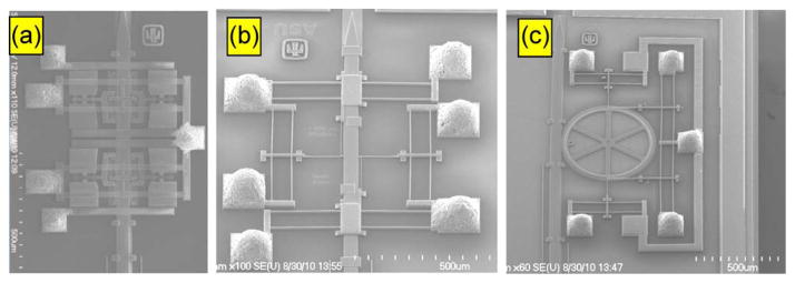
SEM picture showing Ag epoxy bump interconnect on MEMS movable microelectrodes with (a) chevron microactuators, (b) linear actuator, and (c) linear actuators with a gear.
The works presented in this paper are part of our project to develop fully packaged high-density arrays of MEMS movable microelectrodes for single-neuronal recordings. The MEMS chip, as shown in Fig. 1, will be referred to as the testing sample throughout the rest of this paper. The overall MEMS testing die size is 2.8 mm × 6.3 mm. Each die/chip contains three independently actuated electrothermal microactuators, which move the microelectrodes. The MEMS chip is made of polysilicon developed using the SUMMiT V process in Sandia National Laboratories, NM.
The mechanism of movable microelectrode with chevron actuators is shown in Fig. 2. For more details on the operational principles, the reader is referred to our earlier report [28]. Each microelectrode consists of four chevron electrothermal microactuators, two independent microactuators that move the microelectrode either left or right (laterally, along x-axis as shown in Fig. 2), and two independent microactuators to lock the microelectrodes in position and prevent drifting. Each microactuator consists of two sets of four to five thermal strips (made of polysilicon with the width of 1.5 μm) that slightly angled to direct the movement of the microactuator. Each electrode is able to move laterally (along x-axis) with an incremental step of 8.8 μm and a maximum stroke displacement of 5 mm. For chevron design, each microelectrode is actuated by two pulses (named A and B) of current: a pulse A with the duration of 300 ms to open the locking mechanisms and a pulse B with the duration of 100 ms to move the microelectrode. A current of approximately 80 mA is drawn for each pulse. This MEMS chip after appropriate electrical and mechanical packaging steps will be implanted on the rat’s brain for neuronal recordings.
Fig. 2.
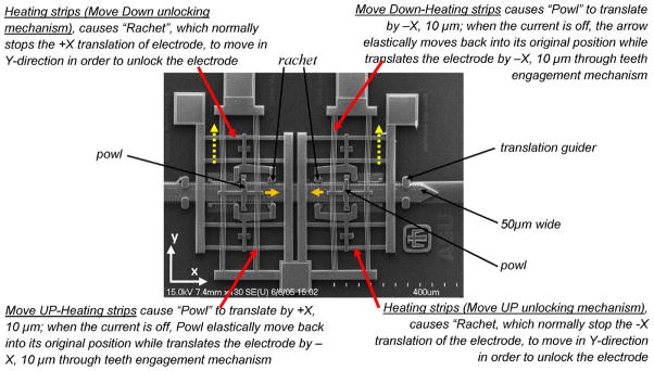
Electrothermally actuated movable microelectrode using chevron actuators.
B. Previous Wire-Bonded Package
Previously, our MEMS chip, as shown in Figs. 1 and 2, was successfully packaged by using Au wire-bonding technique, with the overall package as shown in Fig. 3 [24]. The MEMS package was successfully implanted on the rat’s skull, and the movable MEMS electrodes were capable of recording the single-neuronal activity long-term experiments in Sprague Dawley rats [28]. The overall package of this design was relatively large (more than three times than the actual chip size) and relatively heavy (approximately 5 g) with an overall thickness of approximately 5 mm that does not allow for scaling up the number of movable microelectrodes in the brain to monitor ensembles of neurons. Therefore, an alternative chip-scale package for the MEMS chip was needed that will allow us to scale up the number of MEMS chips on a single package to achieve high-density MEMS movable microelectrodes. Higher numbers of movable microelectrodes are generally desirable for a number of neural recording applications such as neural prostheses, as it enables more precision, accuracy, and fine control of direct brain-controlled neural prosthetic limbs [29], [30].
Fig. 3.
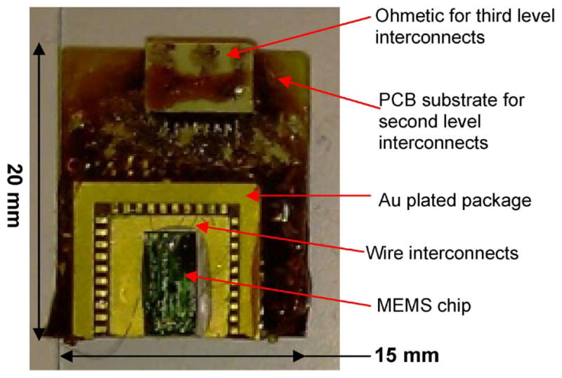
Previous design of wire-bonded package [24].
C. Custom-Made Flip-Chip Machine
Commercially available flip-chip machines from Finetech, Inc., (Tempe, AZ) and Advanced Technology, Inc. (Philadelphia, PA), were found to be nonoptimal for bump creation for FLI, underfill for encapsulation, etc. Therefore, we developed our own custom-made setup to facilitate flip chip for MEMS. The custom-made flip-chip machine was capable of the following: 1) creating interconnect bumps with diameters as small as 100 μm; 2) performing the necessary alignment between the chip, as small as 3 mm × 3 mm, and a transparent substrate (glass or flexible substrates such as polyimide or Parylene) and performing a flip-chip assembly; and 3) creating a hermetic and/or semihermetic encapsulation to protect the MEMS chip against any liquid or ionic contamination. A schematic of custom-made flip-chip machine developed is shown in Fig. 4. The main parts of the flip-chip machine were the following.
Fig. 4.
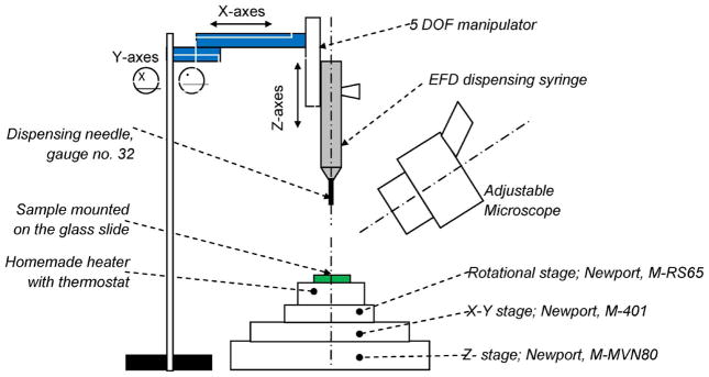
Schematic of the custom-made flip-chip machine.
Three-degree-of-freedom (DOF) stage (X, Y, and Z) and rotational stage, which allowed the mounted chip to be moved and aligned properly, with a maximum translation of 13 mm in X-axes and Y -axes and 8.5 mm in Z-axes.
A custom-made heater with a calibrated J-type thermocouple connected to a thermostat manufactured by Toho Electronics, Inc., model TTM-J4; the heater surface was designed to have a large enough surface to place our testing sample.
A dispensing mechanism manufactured from Engineering Fluid Dispensing (EFD), air power dispenser model Ultimus I. The dispensing tip is a precision stainless steel needle (gauge no. 32) with an inner diameter of 100 μm. The EFD dispensing syringe is attached to a 5-DOF manipulator, which allows the syringe to be adjusted in X-, Y -, and Z-axes and rotation along the X- and Y -axes.
An adjustable stereo zoom microscope manufactured by Leica, Inc., with the maximum magnification of 40 times is capable of viewing the device at an angle. The attachment for the syringe can be replaced by a vacuum attachment to pick up the substrate for alignment with respect to the die. A significant upgrade of this flip-chip machine is currently ongoing that will enable flip-chip assembly for nontransparent substrates and also allow 3-D stacking of combinations of MEMS and IC chips.
D. FLIs—Dispensing Technique
We developed three novel techniques to create FLI bumps connecting the MEMS die to the substrate in flip chip, which are described in our earlier report [23]. In this paper, we used Ag epoxy bump interconnects with a height of approximately 100 μm dispensed on an Al-coated 100 μm × 100 μm polysilicon pads. A SEM picture of MEMS microactuator with Ag bump interconnects is shown in Fig. 5. The Ag bump height is about 100 μm with 10% tolerance prior to packaging; the final collapse height between the die and the substrate after flip-chip packaging ranges from 95 to 105 μm. The bonding shear strength of the Ag bumps as reported earlier [23] is approximately 78 MPa/bump for Ag bump built on 100 μm × 100 μm Al pad.
E. Flip-Chip Assembly Steps
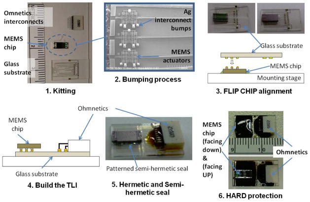
The overall steps involved in the proposed flip-chip packaging approach for the MEMS testing sample using the custom-made machine are shown in Fig. 6. These processes can be extended for packaging other MEMS test samples as well.
Fig. 6.
Steps involved in the packaging of MEMS chip by using flip-chip technology.
Kitting process to prepare the three main components: the MEMS chip, glass substrate, and Omnetics (Omnetics Connector Corporation) third-level interconnects (TLIs).
Bumping process involved dispensing Ag epoxy (E3001; Epoxy Technology, Inc.) on each of the Al pads to create microscale bumps to build the FLIs with a height of approximately 100 μm (a total of 18 bumps per a testing sample).
Flip chip process capable of the following: 1) aligning the die with respect to the transparent glass substrate and 2) bonding the die and substrate together through the FLI Ag bumps. The substeps involved in this process were as follows: 1) The glass substrate was picked up by a suction piston, and 2) the MEMS chip located on the chuck was moved/positioned to align it with the glass substrate. To properly bond the FLI bumps, the glass substrate was positioned on top of the die with a joint pressure of 20–30 MPa/bump. While the Ag epoxy is still wet (uncured), the chuck was then heated up to 120 °C for 1 min to fully cure the Ag epoxy bumps.
Connect the TLI to bond the Omnetics connector to the glass substrate using Ag epoxy. The process was similar to step no. 3.
Create hermetic encapsulation and NHE; in order to create NHE on the front side of the die, hydrophobic silicone microstructures were patterned using the dispensing system as shown in the SEM picture in Fig. 11. Near-hermetic seal was created on the remaining three sides by using the combination of patterned silicone dispensing along the perimeter of the die followed by hard epoxy, explained in the next step.
Hard protection was a process to apply hard epoxy over the die to protect and introduce a near-hermetic seal.
Fig. 11.
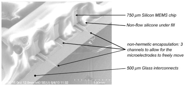
Closed-up SEM picture of the NHE on the front edge of the package.
F. Non-Hermetic Encapsulation (NHE)
To seal the MEMS chip nonhermetically, patterns of nonflow hydrophobic silicone microstructures were created. The 100% silicone was the DAP auto/marine waterproof sealant, which is clear (transparent) and commercially available in the hardware store. EFD dispensing technique, as shown in Fig. 4, was used to pattern the silicone microstructures on the front edge of the die which enable the microelectrode to freely move in and out of the package boundary while simultaneously preventing biological fluids, such as CSF, to enter the MEMS active parts. A test under pressurized liquid immersion was done on the MEMS package after NHE to determine its breakdown pressure as shown in Fig. 7.
Fig. 7.
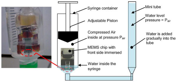
Schematic of the test setup to determine the breakdown pressure of NHE.
G. Black Epoxy Seal
The remaining three sides of the die which were not accessed by the MEMS microelectrodes were sealed by black epoxy. A commercially available epoxy [from Epoxy Technology; mixing two parts, namely, part no. 353ND, part A (90%), and part no. 353ND, part B (10%)] cured at 120 °C for 5 min was used to generate the near-hermetic seal. The literature suggests that the epoxy does not produce a complete hermetic seal as per military standard but rather a near-hermetic seal [19]. At this stage, we have not yet tested the level of hermeticity of the black epoxy seal. A small opening was left on the back side of the die for air ventilation. This air ventilation was necessary to keep the pressure inside the MEMS chip enclosure close to ambient during implantation.
H. Force Measurements on the MEMS Actuator
Force measurements were performed on the packaged MEMS actuator. The MEMS package was held in place using a stereotactic equipment. The packaged MEMS actuator was then lowered by using a 5-DOF micromanipulator. The edge of the MEMS chip was placed at a distance of roughly 1–2 mm from the load cell surface. The load cell (MTC 10/30—ZER; Wipotec, Kaiserslautern, Germany) type was capable of measuring a maximum force of 2 g with a sensitivity of 0.1 mg. The microelectrodes were extended off the edge of the die by approximately 500 μm (along z-axis), leaving a distance of approximately 500 μm (vertically or along z-axis) between the microelectrode and the load cell. The microelectrodes were continuously monitored by a stereo zoom microscope and an LCD monitor. The microelectrodes were actuated further until it pushed down the load cell. The load cell was connected to a computer via a serial connector to send the collected force data in grams.
I. MEMS Implantation on the Rat’s Brain
The packaged MEMS chip was mounted on the rat skull with the microelectrodes implanted in the brain through a craniotomy as shown in Fig. 16. The rats weighed approximately 300 g in weight at the start of the experiment. All animal procedures were carried out with the approval of the Institute of Animal Care and Use Committee, Arizona State University, Tempe. The experiments were performed in accordance with the National Institute of Health guide for the care and use of laboratory animals (1996). All efforts were made to minimize animal suffering and to use only the number of animals necessary to produce reliable scientific data. Prior to the start of the experiment, buprenorphine was administered as an analgesic. The animals were induced using a mixture of (50 mg/mL) ketamine, (5 mg/mL) xylazine, and (1 mg/mL) acepromazine administered intramuscularly with an initial dosage of 0.1 mL/ 100 g body weight and subsequently maintained using 1%–4% isofluorane gas. The rat was attached to a stereotaxic frame (David Kopf Instruments, Tujunga, CA). After the skull was exposed, two stainless steel bone screws (19010-10; Fine Science Tools, Inc., Foster City, CA) were screwed into the skull to act as anchors. A large craniotomy (3 × 2 mm) was drilled with the center point being 2.0 mm lateral to the midline and 2.5 mm posterior to the bregma. After the bone chips were removed, the dura was carefully incised and pulled back away from the center of the craniotomy. The device was mounted on a micromanipulator using beeswax and placed on the open craniotomy. After implantation, dental cement (PMMA) was used to secure the device to the skull.
Fig. 16.

(a) MEMS package #1 (chevron microactuator); picture taken at day 16. (b) Rodent with a MEMS implant on its brain. (c) MEMS package #2 (chevron microactuator); picture taken at day 75.
III. Results
A. Package Size and Weight
The flip-chip technology reduced the final package weight significantly from 4.5 g (using wire-bonding technology) to 0.5 g, which is almost an order of magnitude reduction in the overall assembled weight. Since the weight of the head of an adult rat is approximately 30 g (for a rat weighing 300 g), the aforementioned significant weight reduction will now allow neuronal monitoring without significant impairment to mobility and behavior which is very important in neurophysiological studies. The weight reduction also now allows for scaling up the number of devices and hence numbers of neurons to be monitored in vivo.
As shown in Fig. 8(a) and (b), the flip-chip technology reduced the overall package dimension from “20 mm (L) × 15 mm (W ) × 5 mm (H)” to “12 mm (L) × 9 mm (W ) × 3 mm (H)” with ample space available on the glass substrate that would accommodate one or two more additional chips to be assembled in multichip-on-a-package configuration. As shown in Fig. 8(a) and (b), unlike the wire-bonding technique, the flip-chip technology provided a protection on the MEMS active parts. The MEMS structure could still be seen through the glass substrate, providing a convenient method to visually confirm bonding quality and microelectrode movement under the microscope. The proposed flip-chip technology was used to realize a chip-scale package with glass substrate and flexible Parylene-C interconnects, respectively, as shown in Fig. 8(c) and (d).
Fig. 8.
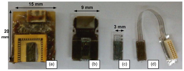
Comparison of the flip-chip and wire-bonding packages. (A) Previous wire-bonding package. (B) MEMS die flip chipped on a glass substrate (reported in this study). (C) Chip-scale flip-chip package. (D) Chip-scale flip chip with flexible Parylene-C interconnects.
B. Electrical Test of Ag Bumps in the Packaged MEMS Devices
Resistance measurements between the bond pads connecting the actuators and ground remained consistent before and after flip chip. The final resistance measurement after flip chip was comparable with the summation of the resistances at the silicon level (in the MEMS chip) and the resistances of the traces in the glass substrate. The electrical resistance of 100 μm (W ) × 100 μm (L) × 100 μm (H) Ag bump was measured using a four-point configuration and was run over 1 million on/off cycles (without failure) at a frequency of 10 Hz with a duty ratio of 50% at current densities ranging from 100 to 400 A/cm2. The results in Fig. 9 and in Table I showed a consistent average resistance of 40 mΩ which was negligible in comparison with the resistance of MEMS electrothermal microstructure (several hundreds of ohms). This result was in agreement with the previously reported electrical test on the Ag bump interconnect [23].
Fig. 9.
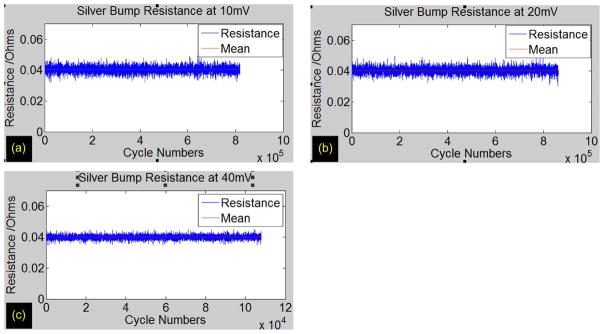
Resistance of Ag bump FLI versus the number of on/off cycles, at 10-Hz frequency and a duty ratio of 50% at (a) 10, (b) 20, and (c) 40 mV.
TABLE I.
Resistance of Ag Bump Interconnects
| 10mA (100A/cm2) | 20mA (200A/cm2) | 40mA (400A/cm2) | |
|---|---|---|---|
| Mean (mOhm) | 40.4 | 40.5 | 40 |
However, the Ag bump resistance of 40 mΩ is relatively high in comparison with Cu pillars that have resistances of 0.8–1 mΩ for similar bump dimensions. Lower bump resistance is desirable for high-speed CMOS I/O application. Work is ongoing in our laboratory to reduce the bump resistance of Ag bumps to levels similar to Cu pillars. The current working hypothesis is that the poor contact resistance between the Ag bump and the Au pad is a significant contributor to the Ag bump resistance. Plans to reduce this contact resistance include controlled cleaning of the Au substrate prior to applying Ag bump and a thicker Au pad, which is currently only 0.25 μm.
C. Microelectrode Movement Test
After the MEMS packaging steps were completed, the microelectrodes were tested for its movement as shown in Fig. 10. For this testing sample, the electrothermal microactuators moved a rotating gear, which, in turn, drove the MEMS microelectrode. To move the microelectrode forward [outside the package boundary, as shown in Figs. 9(b) and 10(a)], a current pulse of 300-ms duration was applied to open the forward-locking mechanism. In the middle of this 300-ms current pulse, another 100-ms pulse of current was applied to move the microelectrode forward by 8.8 μm. The total current required for two sets of pulses was 30 mA. The pulses were applied at the rate of 0.5–1 Hz. The electrode was able to move over a maximum displacement of 5 mm [the condition at Fig. 10(b)]. To move the electrode backward [as shown in Fig. 10(c) and (d)], similar set of pulses was required for backward-locking mechanism and the backward movement actuator.
Fig. 10.
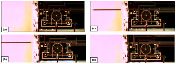
Movement tests of the MEMS microelectrode (linear microactuators with a gear mechanism) after packaging. (a) Forward motion—before actuation. (b) Forward motion—after full-stroke actuation. (c) Reversed motion—halfway of the actuation. (d) Reversed motion—back into the initial resting position.
D. NHE Pictures and Tests
A SEM picture of the NHE on the front side of MEMS die/ package is shown in Fig. 11. The die thickness was 750 μm, and the glass substrate thickness was 500 μm. The channel access for the microelectrode was approximately 150 μm wide and 100 μm high created by patterned silicone microstructures. The glass substrate itself was dip coated with a thin-layer hydrophobic coating. The package was tested in water under constantly increasing water pressure, and it was found that the breakdown pressure of the NHE was 80 cm of water or 7.85 kPa. Micrographs of the patterned hydrophobic silicone on the front side of the package are shown with the MEMS chip facing up and with the MEMS chip facing down in Fig. 12. These patterned silicone microstructures will face the brain surface and be exposed to the CSF after mounting on the skull.
Fig. 12.
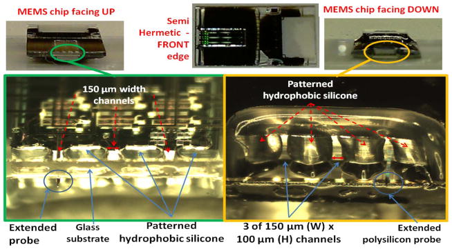
Micrographs of the NHE showing the silicone microstructures; the MEMS die has three movable microelectrodes with chevron microactuators.
Since the primary function of the NHE was to act as a barrier against fluids (CSF, blood, and skin exudates) from the brain, the NHE of the front side of the package was first bench tested by dipping it into the following: 1) a bath of water at room temperature and 2) a bath of artificial CSF that maintained at body temperature (37 °C) while the MEMS microstructure was continuously monitored (by live CMOS camera recording) for any possible leaking. Fig. 13(a) and (b) shows the water-dipping test results before and after two days, respectively. After two days of tests, there was no trace of liquid water contamination on the MEMS chip as confirmed by visual observation under the microscope. As shown in Fig. 14, a subsequent test was conducted by dipping the front face of the package into a bath of purple-colored water while actuating the middle microelectrode up and down at a frequency of 1 Hz. The test was conducted while continuously monitoring for possible water leak using a video camera. After more than 24 h of test (over 86 000 cycles), the MEMS chevron microactuators were still functional, and there was no visible trace of leaking on the MEMS chip.
Fig. 13.
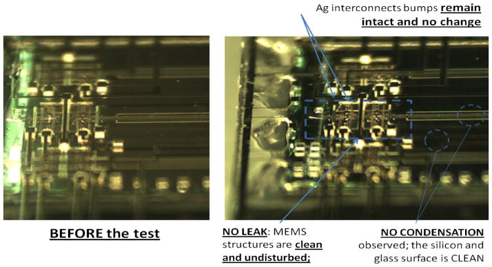
Showing the MEMS chevron microactuator condition (a) before and (b) after the leaking tests by dipping the front edge of the package into a bath of de-ionized water at room temperature for two days.
Fig. 14.
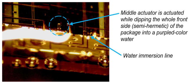
Showing the live picture of the MEMS chevron microactuators that actuate the microelectrode up and down while dipping half of the package into a purple-colored water for more than 24 h (86 000 cycles).
As shown in Figs. 13 and 14, the nonhermetic seal design on the MEMS package was successful in preventing water and CSF entry into the MEMS device. The leak test also showed no visible evidence of wetting of the 150 μm (W ) × 100 μm (H) microchannels due to the large water contact angle of the silicone used in the barrier. The microelectrode with a dimension of 50 μm × 4 μm was relatively small compared to the size of each microchannel; the presence of the fluid turbulence created by repeatedly moving the microelectrode in and out through the microchannels, as shown in Fig. 14, did not break the hydrophobic boundary layer inside the microchannel.
E. Actuation Force Test
The force data for one microelectrode is shown in Fig. 15. The spikes in the data beyond 12 s correspond to the times when the release locks are being activated and the microelectrode is moving down. The forces saturated when the microelectrode could not push the load cell down any further. The force experiment was carried out using chevron MEMS microactuators as shown in Fig. 2.
Fig. 15.
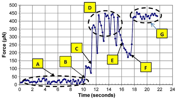
Measurement of actuation force for a MEMS microelectrode with chevron microactuators. (a) Microelectrode is moved toward the load cell’s surface. (b) Tip of microelectrode touched the load cell surface but did not make a good contact. (c) Microelectrode made a good contact and pushed the load cell. (d) Load cell senses the force generated by the thermal microactuator at the rate of 0.5 Hz. (e) Microactuator was turned off; the residual stress on the microelectrode due to the locking mechanism provided the resisting force. (f) Thermal actuator was turned back on and pushed the load cell. (g) Load cell sensed the force generated by the thermal microactuator at the rate of 1 Hz.
F. In Vivo Nonhermetic Test
The packaged MEMS device was placed on an open craniotomy to test for fluid entry and semihermetic encapsulation under chronic conditions. Two MEMS packages were implanted on rats. As seen in Fig. 16(a), the packaged MEMS chip (with a weight of approximately 0.5 g) was held stable for rat #1 for 17 days. The package eventually failed due to a crack on the glass substrate. Fig. 16(c) shows the MEMS package on rat #2, where the package also failed 77 days after implantation due to cracks in the glass substrate. Both packages showed no evidence of liquid or blood contamination at the time of failure. The results indicated that NHE was potentially suitable for chronic experiments.
G. Three-Dimensional Stacks of Flip-Chip Devices
One of the advantages of flip-chip packaging is the ability to scale up the number of chips without necessarily increasing the X-Y form factor by facilitating 3-D stacks. The current study is extended to realize a chip-scale 3-D stack using flip-chip technology and packaging processes detailed in Fig. 6. A 3-D flip-chip stack, where one MEMS die containing the same mechanical structures (chevron microactuators) as the one shown in Fig. 2 is bonded/flip chipped on top of the other by using Ag bumps (a total of 18 bumps/die), is shown in Fig. 17. A 3-D stack of two dies is shown in Fig. 17(a), where the base die is flip chipped on the glass substrate for electrical connection and the second die is flip chipped on the back side of the first die. A 3-D stack with three dies is shown in Fig. 17(b) after the third die is flip chipped on top of the second die.
Fig. 17.
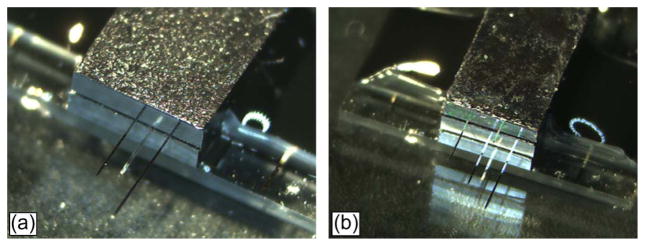
(a) 3-D MEMS packaging with two stacks of flip-chip dies and (b) 3-D MEMS packaging with three stacks of flip-chip dies.
While the second and third dies are not yet electrically connected [as shown in Fig. 17(a) and (b)], the results demonstrate the ability to use the current flip-chip packaging technique and processes to realize 3-D flip-chip stacks. We are currently working on different options for electrical interconnects, such as 3-D through-silicon via, interposer and second-level interconnect bumps, and flexible Parylene interconnects to electrically connect these 3-D stacks of dies.
Following the processing steps as shown in Fig. 6, black epoxy (step no. 6) is applied on each layer of die as shown in Fig. 17. There is a possibility of reducing the packaging steps by applying the step no. 6 after all dies are fully flip chipped. To achieve this, dies will have to be stacked in 3-D fashion using Ag bumps that mechanically connect/bond one die to the other. While this may potentially lead to more efficient processes, the mechanical strength that Ag bumps can handle remains a concern as more dies are stacked. The amount of force needed to totally shear/detach the top die in a 3-D stack from the die immediately underneath as a function of the numbers of dies in the stack is shown in Fig. 18(a). The first and second trials are for the case where there is no epoxy encapsulation applied to the package. The shear force was measured using a load cell with an accuracy of 1 g and a maximum reading of 1000 g. The apparatus was attached to the top die, and the whole package was attached to an X, Y, Z stage. While the stage was moved along the X-direction, the apparatus experienced a reaction force that sheared the interconnect bumps until they failed. As the die is fully sheared or detached, the failed bumps are observed under the microscope to identify the cause of failure. The results of the visual analysis under the microscope are summarized in Table II (Fig. 19).
Fig. 18.
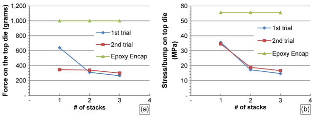
(a) Minimum force needed to fully shear/detach the top die as a function of number of dies in a stack. (b) Minimum stress/bump experienced by the top die as a function of number of stacks.
TABLE II.
Summary of the Visual Inspection on the Failed Bumps of the 3-D Stacks
| # of die in the stacks | Failure location | Condition | Details results |
|---|---|---|---|
| 1 | Ag bump | 1st trial – no epoxy | 18 bumps are failed: most failures are close to the interface b/w Al pad and Ag bump; some failures are close to the interface b/w Au pads and Ag bump; no failure on the polysilicon; see sample in Fig. 19A |
| 1 | Ag bump and poly pads | 2nd trial – no epoxy | 10 out of 18 bumps are failed on the polysilicon pads - suggesting that this particular die may have a prior fabrication issue which impact its polysilicon strength; 8 bumps are failed on the interface b/w Au pad and Ag bump |
| 1 | No failure | Epoxy encapsulation | 18 bumps are still intact with no visible issue; the amount of force required to fail the package exceed the ability for the current testing method. 1,000 g |
| 2 | Adhesion of Ag and Si surface | 1st trial | The failure is on the 2nd die (top). All 18 bumps show same the signature of failure – on the interface b/w Ag bumps and Si-die. Suggesting a poor adhesion b/w Ag and bare Si-surface; the base (1st die) is still attached strongly even though it experiences more magnitude of combination - shear and bending strength; see sample in Fig. 19B |
| 2 | Adhesion of Ag and Si surface | 2nd trial | The failure is on the 2nd die (top); Same signature as the 1st trial. |
| 2 | No failure | Epoxy encapsulation | 18 bumps are still intact with no visible issue; the amount of force required to fail the package exceed the ability for the current testing method. 1,000 g |
| 3 | Adhesion of Ag and Si surface | 1st trial | Failed on the 3rd die, all 18 bumps are showing the same signature of failures, which is at the interface between the Ag bump and the Si bare die (non polished surface); see sample in Fig. 19A |
| 3 | Adhesion of Ag and Si surface | 2nd trial | Both 2nd and 3rd die are failed, cannot really tell which die that failed first; It is believed that the 3rd die failed first and its impact trigger the 2nd die; Same failure signature as the 1st trial. |
| 3 | No failure | Epoxy encapsulation | 18 bumps are still intact with no visible issue; the amount of force required to fail the package exceed the ability for the current testing method. 1,000 g = 4 x the weight of adult rat |
Fig. 19.
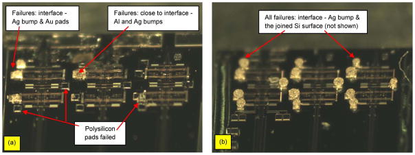
(a) Failed sample failure on the base die showing three kinds of failures. (b) Failed sample on the second die showing one type of failure at the interface between Ag bump and the joined Si bare die surface (not shown).
Fig. 18(b) shows the amount of shear stress experienced by each bump when the top die failed. The shear stress was obtained by dividing the total amount of force, as shown in Fig. 18(a), by the total amount of area of failed Ag bumps. As shown in Table II, for one stack, most of the bump failures are close to the interface between the Al surface and the Ag bumps. This type of failure signature is similar to the failure when each Ag bump is individually sheared. The breakdown shear stress/bump on one-stack configuration is around 35 MPa, which is significantly lower than the breakdown shear stress/ bump when each is individually sheared (78 MPa). As more stacks are applied (two dies or more), the shear strength/bump is reduced to the level of 18–20 MPa, which is mainly caused by poor adhesion between Ag bumps and rough Si surface.
As shown in Fig. 18(a), when the epoxy encapsulation is applied, the force required to shear the top die exceeds the maximum force capacity of 1000 g for the load cell used. As expected, the epoxy encapsulation provides a significant improvement on the mechanical strength of the 3-D stacks. Visual inspection on the base die (bottom die) shows that Ag interconnects are attached to the glass substrate with no sign of failure.
IV. Discussion
In this report, a MEMS testing sample consisting of MEMS movable microelectrode was used to demonstrate a novel flip-chip packaging and NHE approach. The electromechanical operations of these electrodes involved electrothermal heat strips with a minimum dimension of 2 μm and ratchets and pawls that moved a 6-mm-long microelectrode with a 50 μm × 4 μm cross section resting on the surface of the die. The bond pads were approximately 75 μm from the nearest mechanical structures. The mechanical complexity of the MEMS structures in the test sample and the successful creation of FLI in such close proximity to complex mechanical structures make the packaging approach demonstrated here more broadly applicable to other types of MEMS chips.
The change of packaging technique from wire bonding into flip chip reduced the package dimensions and weight significantly from 4.5 to 0.5 g or less (depending on the thickness and material of the substrate) as shown in Fig. 8. Furthermore, an extra encapsulation by using a thin transparent glass was required in the prior wire-bonding method to cover and protect the bonded wires as shown in Fig. 3. The custom-made flip-chip machine demonstrated was still in the research and development stages, where the operation was completely manual capable of producing approximately ten fully packaged MEMS in one day depending on the skill of the user. We are currently upgrading this machine to a more automated operation to achieve higher throughput.
Dispensing technique was used to create 100-μm-high Ag bumps; the process steps for these Ag bumps were explained previously [23]. The Ag bump FLI can potentially be applied either at the chip or wafer level for packaging. While, in this study, we have only shown a 100-μm-diameter bump with a gap of 100 μm, this FLI technology has been proven to work for 50-μm-diameter bump with the gap of 50 μm. Currently high-end CPU uses Cu bump/pillar as the interconnects with 45-μm diameter and 45-μm gap. We are currently working to further improve the FLI technology to create 25-μm-diameter bumps with a gap of 25 μm for fine-pitch flip-chip integration. The packaging processes reported here did not include the wafer dicing step because the testing sample was received after dicing and after release. It is possible that wafer dicing, which is often considered as the most destructive process in MEMS, might impact the packaging steps reported here. We are currently developing a wafer-scale approach for MEMS packaging using the techniques reported here.
The microelectrodes were extended outside the MEMS boundary to penetrate the brain tissues after implantation for neuronal recordings. Similar situations exist for a number of MEMS sensor devices such as pressure sensors, glucose sensors [31], and chemical sensors [32] that require some access to the external environment. In the current study, the size of the clearances in the silicone microstructures (to allow microelectrode access) and the hydrophobic nature of these microstructures seemed adequate to prevent fluid entry through these pores until a breakdown pressure of 80 mm of water as shown in Fig. 7. This pressure is significantly larger than the intracranial pressure of the brain (6.5–18 cm of water [33] in human).
The NHE was also tested by dipping the MEMS package into a bath of purple-colored water while actuating the microelectrode up and down. The rationale of actuating these microelectrodes was to break the potential boundary layer formed at the opening in the silicone microstructures and increase the chance of turbulence that might help the water to enter the MEMS active part. The test was carried out for more than 24 h, which translated to more than 86 000 up and down cycles at the frequency of 1 Hz. The results showed no visible entry of water/liquid and/or contamination on the MEMS active part. One may argue that there was still a chance for water vapor or moisture to contaminate the MEMS enclosure driven by the humidity difference between the water bath and the MEMS enclosure. However, it was expected that the moisture contamination or the increase of humidity inside the MEMS enclosure was minimal because ventilation was provided on the back of the die for the ambient air to circulate in and out of the MEMS enclosure.
After the MEMS chip was completely packaged, the MEMS microelectrode was tested for its force generation. Because the load cell can only detect uniaxial force, microelectrode buckling might have introduced some inaccuracy in the force reading. It is quite likely that the forces shown in Fig. 15 were marginally less than the actual forces exerted by the microactuators on the microelectrodes. The force generated by the MEMS microelectrode was approximately 450 μN, as shown in Fig. 15, which is sufficient to move the microelectrode inside the brain tissue. Jensen et al. showed that it required approximately 180 μN to move the microelectrode once the electrode was approximately 2 mm deep in the rat cerebral cortex [34], [35].
Results of an in vivo study to test the NHE are shown in Fig. 16. Two rats were tested with the same MEMS implant. The MEMS package on rat #1 showed failure after 17 days of implant. The failure was not due to a failure in the semihermetic encapsulation but rather due to a crack on the glass package. Visual observation on the MEMS package under the microscope after 17 days showed no evidence of blood or fluid penetration into the MEMS active part. The MEMS structures and Ag bump joints remained clean and intact. MEMS package on rat #2 showed failure after 77 days of implant. Again, the failure was due to cracks on the glass package. There was no evidence of contamination on the MEMS chip. Mechanical stresses induced during rat behavior were most likely responsible for the cause of cracks in the glass substrate. Such failures can be mitigated by increasing the thickness of the glass substrate from 0.5 to 1 mm or higher and provide an outer foam encapsulation to cushion the impact of behavioral collisions.
The flip-chip packaging processes introduced in this paper include the following three steps that could potentially result in outgassing: 1) the curing process of Ag epoxy in the FLI at 120 °C for 1 min; 2) the curing process of silicone microstructures at room temperature for 24 h; and 3) the curing process of the black epoxy (hard protection) at room temperature for 24 h. The aforementioned sequence of packaging steps was tested on the MEMS device that consisted of a highly sensitive movable microactuator fabricated using the SUMMiTV process in Sandia National Laboratories, NM, with the minimum feature size of less than 2 μm. The microelectrode (50 μm wide and 4 μm thick) sat directly on the die’s surface and moved along the “in-plane (x-axis)” direction. A thin layer of surface contamination on the path of microelectrode which is movable can potentially jam/freeze the microelectrode’s movement. A solid particulate contamination in or on the MEMS active structure would impede, hinder, or choke the electrothermal microstructures, which are suspended 2 μm above the die’s surface. The postprocessing inspection at every step of the flip-chip packaging process showed that there was no visible surface contamination of the active MEMS structures after the Ag epoxy bumping step, silicone curing, and black epoxy curing. The MEMS devices were tested for function before (by using a probe station) and after the packaging processes were completed. The static (one-increment-step movement of 10 μm) and dynamic (moved at 10-Hz frequency with the maximum stroke of 5 mm) results showed that the possible outgassing that occurs during the flip-chip packaging processes creates no apparent detrimental effect on the MEMS functionality.
The Ag FLI introduced in this paper adheres well mechanically with a variety of surfaces including Al, a CMOS standard metallization that normally does not adhere well with solder paste. Under bump metallization (UBM) is normally needed to mechanically and electrically connect the Al-based metal layers to Cu pillar or solder bumps. Ag bump, introduced in this paper, does not require UBM as it performs a strong mechanical contact with Al pad with the shear strength of 78 MPa and forms a good electrical interconnect with Al pad with negligible contact resistance.
In the case of 3-D stacks of MEMS dies, the mechanical shearing force—that bonds the top die to the die underneath—decreases as more stacks are applied when there is no epoxy encapsulation as shown in Fig. 18(a). While the base (bottommost) die experienced the greatest amount of load (a combination of shear force, bending, and torsion), the first die (on the top) failed first. This result was rather counterintuitive. Visual inspection under the microscope showed that the failure was caused by poor adhesion between the Ag bumps and the Si-die surface, which was rough (nonpolished). The coarse Si surface roughness causes a poor quality of contact with the Ag bumps during the reflow process, which leads to a lower bonding strength. To significantly improve the bonding strength, one must polish the back side of the wafer and provide adhesion layer such as Ti/Cu that adheres well with most metallic joints, including Ag bumps. The breakdown shear stress/bump on one-stack configuration is around 35 MPa, which is significantly lower than the breakdown shear stress/bump when each is individually sheared (78 MPa). When a die is sheared, all bumps (18 in total) experienced not only shear stress but also bending stress. Furthermore, an avalanche effect may occur as the load is applied to the die where failure in one bump increased the loading stress on the remaining bumps, which led to failures in more bumps.
We had reported a novel MEMS microflex interconnect (MMFI) technology earlier [36] to create chip-scale packaging and interconnect for MEMS chips. The present approach using flip chip provides significant advantages over the previous MMFI approach. Briefly, MMFI involved sandwiching a flexible polyimide interconnect between two gold stud bumps in a rivet-bonding mechanism on the electrical bond pads on the die. The polyimide interconnect was locked in place by vias etched through the substrate at the center of each bond pad. These holes in the polyimide substrate were then aligned with the gold stud bumps on the die, and a second gold stud bump was placed on top of the first stud bump to lock the polyimide substrate. The MMFI method provided an attractive approach to develop a flexible interconnect scheme for MEMS chips with the following features: 1) a 15–20-μm clearance between the silicon die and polyimide substrate which was adequate for the mechanical structures to operate without hindrance and 2) a high reliability. The current flip-chip packaging and interconnect approach performs better than the MMFI in the following aspects. When there are a large number of bond pads, MMFI becomes rather tedious, and small errors in the placement of stud bumps leading to off-center bumps on the bond pads of the die lead to significant difficulties in aligning all the holes (bond pads) in the flexible interconnect with the corresponding stud bumps on the die. Furthermore, since the stud bumps were done sequentially, it led to random errors in the stud-bump placement as opposed to a systematic bias in the relative position of all the individual stud bumps with respect to the bond pads. Unfortunately, the former type of error can be sometimes catastrophic for successful interconnects leading to lower yield in the process. The flip-chip-based technology described here is a much simpler process that scales very well with increasing number of bond pads. More importantly, off-center bumps do not impact the functionality of the interconnect. Additionally, the flip-chip-based process described here can achieve a clearance of 100 μm or more since it allows for the creation of high-aspect-ratio FLI bumps.
Unlike the previously reported flip-chip packaging designs by Erismis et al. [25], Panchawagh et al. [14], and Dy and Ho [27], the flip-chip packaging approach introduced in this paper contains the following distinct novelties that can be summarized as follows.
The flip-chip technology introduced in this paper provides not only the protection to the MEMS active devices but also the electrical interconnect from the MEMS die to the substrate through Ag FLI bumps. This latter function eliminates the need of additional wire-bonding technique which may not be the best interconnect for long-term biomedical application.
The NHE technique introduced in this paper to protect the MEMS active mechanism against liquid (water) contamination was developed without the need of additional microfabrication process that must be incorporated in the MEMS foundry. This advantage makes this NHE more general and can be used for a wide MEMS application.
The flip-chip bonding involved a low-temperature curing process at 120 °C for 1 min, which is relatively safe for most MEMS devices and packages. The low-temperature and short-time curing process reduces the potential residual stress and promote energy-efficient process.
The large clearance between Si die and substrate—that can be tailored (25–100 μm) depending on the height of Ag bumps [23]—provide the following: 1) a forgiving tolerance in the flip-chip process against prior substrate defects (such as large bowing that is more than the tolerance specifications) and 2) the potential ability to use a flexible substrate such as polyimide and Parylene.
V. Conclusion
In this paper, a flip-chip-based packaging approach for a MEMS chip with complex mechanical gears and actuators has been described. The packaging technology reduced the overall package size and weight significantly from 5 (from the previously designed wire-bonded package) to 0.5 g. In order to mechanically and electrically connect the MEMS chip to the glass substrate, previously reported Ag bumps [23] were used, which provide approximately 100-μm clearance between the die and the substrate surfaces. The clearance was more than adequate to allow free movement of the electrothermal heat strips, microelectrodes, ratchets, pawls, and other mechanical structures on the die. To protect the MEMS active structure from possible contamination from CSF, blood, and skin exudates after the animal implantation while allowing accesses for three microelectrodes to move in and out of the package boundary, an NHE was created on the front side of the package. Bench top testing and in vivo testing of fully packaged MEMS devices demonstrated the success of the flip-chip interconnects and the NHE. The results from in vivo testing show no trace of contamination from the CSF to the MEMS structure for over 17 and 77 days, respectively. The packages failed due to cracks of the glass substrate caused by the active animal behavior. The flip-chip approach also proposed here also enabled the development of mechanically stable 3-D stacks of MEMS chips providing an exciting opportunity to scale up the number of MEMS microelectrodes for brain implant application.
Acknowledgments
This work was supported by the National Institutes of Health under Grants RO1NS055312 and RO1NS055312-S1.
The authors would like to thank the Center for Solid State Electronics Research, Arizona State University, Tempe, for the use of their clean room facilities.
Biographies
 Jemmy Sutanto (M’01) received the B.S. and M.S. degrees in mechanical engineering from RMIT University, Melbourne, Australia, and the Ph.D. degree in mechanical engineering from Georgia Institute of Technology, Atlanta.
He was a Senior Packaging Engineer with Intel Corporation with expertise in the high-density first-level interconnects for high-end CPU. He was then an Associate Research Scientist with the School of Biological and Health Systems Engineering, Arizona State University, Tempe. He is currently with Amkor Technology, Chandler, AZ, as a Program Manager for fine-pitch (< 40 μm) Cu pillar, chip-on-chip, and chip-on-wafer technologies. He has been the author or a coauthor of 16 journal papers and one book chapter. He is the holder of one U.S. patent, two trade secrets, and five patent pending. His research experience is in the areas of microelectromechanical systems (MEMS), bio-MEMS, and microelectronics/MEMS packaging.
Dr. Sutanto is a member of the American Society of Mechanical Engineers and the Biomedical Engineering Society.
 Sindhu Anand received the B.E. (Hons.) degree in electrical engineering and the M.Sc. (Hons.) degree in biological sciences in 2008 from Birla Institute of Technology and Science, Pilani, India, and the M.S. degree in biomedical engineering from Arizona State University, Tempe, in 2011, where she is currently working toward the Ph.D. degree in biomedical engineering specializing in the neuroengineering track.
Her research interests include the development of robotic implantable technologies, the design of neural interfaces, and biological microelectromechanical systems.
 Arati Sridharan received the M.S. and Ph.D. degrees in bioengineering from Arizona State University, Tempe, in 2007 and 2009, respectively.
Her research efforts were in the area of photonic interfaces for biosensors. She is currently a National Institutes of Health Ruth L. Kirschstein Postdoctoral Fellow with the Neural Microsystems Laboratory, Arizona State University. Her research interests include the development of biocompatible and mechanically compliant coatings for stable neural interfaces.
 Robert Korb received the B.S. degree in aeronautical engineering from The Ohio State University, Columbus, and the B.S. degree in electrical engineering and the M.S. degree in biomedical engineering in 2011 from Arizona State University, Tempe, where his research experience included microelectromechanical systems packaging.
He spent nine years in the semiconductor industry with STMicroelectronics as a Yield Analysis and Test Engineer. He is currently with the School of Biological and Health Systems Engineering, Arizona State University.
 Li Zhou received the B.S. degree in electrical engineering from Huazhong University of Science and Technology, Wuhan, China, in 2010. He is currently working toward the M.S. degree in electrical engineering in the School of Electrical, Computer and Energy Engineering, Arizona State University, Tempe. His M.S. thesis involves the design of wireless systems on package with 3-D stack technique for microelectromechanical systems movable microelectrodes.
He is proficient with digital circuits and VLSI circuits design and verification.
 Michael S. Baker received the B.S. and M.S. degrees in mechanical engineering from Brigham Young University, Provo, UT, in 1999 and 2002, respectively.
His research efforts were in the area of on-chip actuation of microelectromechanical systems (MEMS) bistable mechanisms. He is currently a Principal Member of Technical Staff, Advanced MEMS Department, Sandia National Laboratories, Albuquerque, NM. His research interests in MEMS include compliant mechanism design, acceleration switches, relays, and methods of actuation.
 Murat Okandan (M’98) received the Ph.D. degree from Pennsylvania State University, University Park.
Since 1999, he has been with Sandia National Laboratories, Albuquerque, NM, where he is a Principal Member of Technical Staff and has been involved in microelectronics and microsystems with expertise in solid-state device physics, microelectronics processing, and sensors. He has been contributing to and leads several projects ranging from biomedical (DOE Artificial Retina Program and NIH Actuated Neural Probes Program) to extreme environment/highly sensitive physical sensors (shock sensors for energetic materials, atomic magnetometer, microseismometer, and gravimeter) and microsystems-enabled renewable energy, all leveraging the unique capabilities provided by microsystems. He has authored or coauthored over 30 publications, is the holder of 14 patents, and has nine patents pending and numerous invention disclosures.
 Jit Muthuswamy (M’00–SM’11) received the M.S. degree in electrical engineering and the M.S. and Ph.D. degrees in biomedical engineering from Rens-selaer Polytechnic Institute, Troy, NY.
He is currently with Arizona State University, Tempe, where he is an Associate Professor of bio-engineering with the School of Biological and Health Systems Engineering and an Affiliate Faculty in electrical engineering. His research program in developing novel neural interfaces has been supported by NIH, Whitaker Foundation, Defense Advanced Research Programs Agency, and the Arizona Biomedical Research Commission. His research interests are in neural engineering, neural interfaces, and biological microelectromechanical systems.
Dr. Muthuswamy is a member of the Society for Neuroscience. He was a recipient of the Excellence in Neural Engineering Award at the Joint International Conference of the Biomedical Engineering Society and the IEEE Engineering in Medicine and Biology Society in 2002 and the Outstanding Paper Award (along with coauthor and student, Nathan Jackson) at the the 41st Annual International Microelectronics and Packaging Society Symposium in 2008.
Footnotes
Color versions of one or more of the figures in this paper are available online at http://ieeexplore.ieee.org.
Contributor Information
Jemmy Sutanto, Email: jsutanto@asu.edu, School of Biological and Health Systems Engineering, Arizona State University, Tempe, AZ 85287-9709 USA.
Sindhu Anand, Email: sanand8@asu.edu, School of Biological and Health Systems Engineering, Arizona State University, Tempe, AZ 85287-9709 USA.
Arati Sridharan, Email: asridhar@asu.edu, School of Biological and Health Systems Engineering, Arizona State University, Tempe, AZ 85287-9709 USA.
Robert Korb, Email: rtkorb@asu.edu, School of Biological and Health Systems Engineering, Arizona State University, Tempe, AZ 85287-9709 USA.
Li Zhou, Email: lzhou37@asu.edu, School of Electrical, Computer and Energy Engineering, Arizona State University, Tempe, AZ 85287-5706 USA.
Michael S. Baker, Email: msbaker@sandia.gov, Sandia National Laboratory, Albuquerque, NM 87185 USA
Murat Okandan, Email: mokanda@sandia.gov, Sandia National Laboratory, Albuquerque, NM 87185 USA.
Jit Muthuswamy, Email: jit@asu.edu, School of Biological and Health Systems Engineering, Arizona State University, Tempe, AZ 85287-9709 USA.
References
- 1.Gilleo K. MEMS and MOEMS packaging challenges. J Mater Process Manuf Sci. 2001;8:361–379. [Google Scholar]
- 2.Grace RH, Maher MA. Electronic Products (Magazine); Sensors & Tranducers. 2010. MEMS: Think outside the chip at the package level; pp. 1–2. [Google Scholar]
- 3.Imhoff AC. Packaging technologies for RFICs: Current status and future trends. Proc. IEEE RFIC Symp.; Anaheim, CA. 1999. pp. 7–10. [Google Scholar]
- 4.Kim YK, Kim EK, Kim SW, Ju BK. Low temperature epoxy bonding for wafer level MEMS packaging. Sens Actuators A, Phys. 2008 May;143(2):323–328. [Google Scholar]
- 5.Monajemi P, Joseph PJ, Kohl PA, Ayazi F. Wafer-level MEMS packaging via thermally released metal–organic membranes. J Micromech Microeng. 2006 Apr;16(4):742–750. [Google Scholar]
- 6.Sidawi D. Diverse solutions tackle MEMS packaging challenges. R&D Mag. 2003 Sep;45:21–23. [Google Scholar]
- 7.Esashi M. Wafer level packaging of MEMS. J Micromech Microeng. 2008 Jul;18(7):073001. [Google Scholar]
- 8.Tilmans HAC, Van de Peer MDJ, Beyne E. The indent reflow sealing (IRS) technique—A method for the fabrication of sealed cavities for MEMS devices. J Microelectromech Syst. 2000 Jun;9(2):206–217. [Google Scholar]
- 9.Berthold A, Vellekoop MJ. IC-compatible silicon wafer-to-wafer bonding. Sens Actuators A, Phys. 1997 May;60(1–3):208–211. [Google Scholar]
- 10.Zhang XX, Raskin JP. Low-temperature wafer bonding: A study of void formation and influence on bonding strength. J Microelectromech Syst. 2005 Apr;14(2):368–382. [Google Scholar]
- 11.Zhang XX, Raskin JP. A dynamic study for wafer-level bonding strength uniformity in low-temperature wafer bonding. Electrochem Solid State. 2005 Aug;8(10):G268–G270. [Google Scholar]
- 12.Tao Y, Malshe AP, Brown WD. Selective bonding and encapsulation for wafer-level vacuum packaging of MEMS and related micro systems. Microelectron Reliab. 2004 Feb;44(2):251–258. [Google Scholar]
- 13.Dixon-Warren SJ. M. I. Group, editor. MEMS Blog. Vol. 2011. MEMS Industry group; 2009. Chipworks: Inside Analog Devices’ new MEMS strategy. [Google Scholar]
- 14.Panchawagh HV, Faheem FF, Herrmann CF, Serrell DB, Finch DS, Mahajan RL. A flip-chip encapsulation method for packaging of MEMS actuators using surface micromachined polysilicon caps for BioMEMS applications. Sens Actuators A, Phys. 2007 Feb;134(1):11–19. [Google Scholar]
- 15.Faheem FE, Gupta KC, Lee YC. Flip-chip assembly and liquid crystal polymer encapsulation for variable MEMS capacitors. IEEE Trans Microw Theory Tech. 2003 Dec;51(12):2562–2567. [Google Scholar]
- 16.Kim KS, Ha CW, Jang TY, Joung SW, Yun WS. Using lateral vibration for thermosonic flip-chip interconnection with anisotropic conductive film. J Micromech Microeng. 2010 Oct;20(10):105 015. [Google Scholar]
- 17.Pai RS, Walsh KM. The viability of anisotropic conductive film as a flip chip interconnect technology for MEMS devices. J Micromech Microeng. 2005 Jun;15(6):1131–1139. [Google Scholar]
- 18.Gui C, Albers H, Gardeniers JGE, Elwenspoek M, Lambeck PV. Fusion bonding of rough surfaces with polishing technique for silicon micromachining. Microsyst Technol. 1997;3:122–128. [Google Scholar]
- 19.Lin LW. MEMS post-packaging by localized heating and bonding. IEEE Trans Adv Packag. 2000 Nov;23(4):608–616. [Google Scholar]
- 20.Tong QY, Gosele U. Semiconductor wafer bonding—Recent developments. Mater Chem Phys. 1994 Mar;37(2):101–127. [Google Scholar]
- 21.Tong QY, Huang LJ, Gosele UM. Transfer of semiconductor and oxide films by wafer bonding and layer cutting. J Electron Mater. 2000 Jul;29(7):928–932. [Google Scholar]
- 22.Campabadal F, Carreras JL, Cabruja E. Flip-chip packaging of piezoresistive pressure sensors. Sens Actuators A, Phys. 2006 Nov;132(1):415–419. [Google Scholar]
- 23.Sutanto J, Anand S, Patel C, Muthuswamy J. Novel first-level interconnect techniques for flip-chip on MEMS devices. J Microelectromech Syst. 2012 Feb;21(1):132–144. doi: 10.1109/JMEMS.2011.2171326. [DOI] [PMC free article] [PubMed] [Google Scholar]
- 24.Jackson N, Anand S, Okandan M, Muthuswamy J. Nonhermetic encapsulation materials for MEMS-based movable microelectrodes for long-term implantation in the brain. J Microelectromech Syst. 2009 Dec;18(6):1234–1245. doi: 10.1109/jmems.2009.2030075. [DOI] [PMC free article] [PubMed] [Google Scholar]
- 25.Erismis MA, Neves HP, De Moor P, Puers R, Van Hoof C. A water-tight packaging of MEMS electrostatic actuators for biomedical applications. Microsyst Technol. 2010 Dec;16(12):2109–2113. [Google Scholar]
- 26.Erismis MA, Neves HP, De Moora P, Puersb R, Van Hoof C. Low voltage electrostatic inchworm actuators in aqueous environments. Proc. Eurosens. XXIII Conf; 2009. pp. 686–689. [Google Scholar]
- 27.Dy E, Ho CM. Development of a cytomic force transducer for experimental mechanobiology. Proc. IEEE 22nd Int. Conf. Micro Electro Mech. Syst; Sorrento. 2009. pp. 391–394. [Google Scholar]
- 28.Jackson N, Sridharan A, Anand S, Baker M, Okandan M, Muthuswamy J. Long-term neural recordings using MEMS based movable microelectrodes in the brain. Frontiers Neuroeng. 2010;3:1–13. doi: 10.3389/fneng.2010.00010. [DOI] [PMC free article] [PubMed] [Google Scholar]
- 29.Moritz CT, Fetz EE. Volitional control of single cortical neurons in a brain–machine interface. J Neural Eng. 2011 Apr;8(2):025017. doi: 10.1088/1741-2560/8/2/025017. [DOI] [PMC free article] [PubMed] [Google Scholar]
- 30.Moritz CT, Perlmutter SI, Fetz EE. Direct control of paralysed muscles by cortical neurons. Nature. 2008 Dec;456(7222):639–642. doi: 10.1038/nature07418. [DOI] [PMC free article] [PubMed] [Google Scholar]
- 31.Kudo H, Sawada T, Kazawa E, Yoshida H, Iwasaki Y, Mitsubayashi K. A flexible and wearable glucose sensor based on functional polymers with soft-MEMS techniques. Biosens Bioelectron. 2006 Oct;22(4):558–562. doi: 10.1016/j.bios.2006.05.006. [DOI] [PubMed] [Google Scholar]
- 32.Sohn YS, Goodey A, Anslyn EV, McDevitt JT, Shear JB, Neikirk DP. A microbead array chemical sensor using capillary-based sample introduction: Toward the development of an ‘electronic tongue’. Biosens Bioelectron. 2005 Aug;21(2):303–312. doi: 10.1016/j.bios.2004.08.050. [DOI] [PubMed] [Google Scholar]
- 33.Steiner LA, Andrews PJ. Monitoring the injured brain: ICP and CBF. Br J Anaesth. 2006;97(1):26–38. doi: 10.1093/bja/ael110. [DOI] [PubMed] [Google Scholar]
- 34.Jensen W, Hofmann UG, Yoshida K. Assessment of subdural insertion force of single-tine microelectrodes in rat cerebral cortex. Proc. 25th Ann. Int. Conf. IEEE-Eng. Med. Biol. Soc; Cancun, Mexico. 2003. pp. 2168–2171. [Google Scholar]
- 35.Jensen W, Yoshida K, Hofmann UG. In-vivo implant mechanics of flexible, silicon-based ACREO microelectrode arrays in rat cerebral cortex. IEEE Trans Biomed Eng. 2006 May;53(5):934–940. doi: 10.1109/TBME.2006.872824. [DOI] [PubMed] [Google Scholar]
- 36.Jackson N, Muthuswamy J. Flexible chip-scale package and interconnect for implantable MEMS movable microelectrodes for the brain. J Microelectromech Syst. 2009 Apr;18(2):396–404. doi: 10.1109/JMEMS.2009.2013391. [DOI] [PMC free article] [PubMed] [Google Scholar]


