Abstract
The capability to perform high-resolution, wide field-of-view (FOV) microscopy imaging is highly sought after in biomedical applications. In this paper, we report a wide FOV microscopy system that uses a closed-circuit-television (CCTV) lens for image relay and a flatbed scanner for data acquisition. We show that such an imaging system is capable of capturing a 10 mm × 7.5 mm FOV image with 0.78 µm resolution, resulting in more than 0.5 billion pixels across the entire image. The resolution and field curve of the proposed system were characterized by imaging a USAF resolution target and a hole-array target. To demonstrate its application, 0.5 gigapixel images of histology slides were acquired using this system.
OCIS codes: (120.4820) Optical systems, (170.0180) Microscopy, (170.4730) Optical pathology
1. Introduction
The conventional microscope architecture generally consists of a microscope objective for light collection from a sample slide, intermediate relay optics, and paired or single eyepieces that project a magnified image of the sample into the eyes. With the advancement of digital cameras, the eyepiece segment of the microscope has been adapted to enable electronic imaging using appropriate optics and cameras. Over the past decades and with the broad acceptance of infinity correction, the conventional microscope design has achieved extensive standardization across the microscopy industry such that objectives and eyepieces from the major microscope makers are largely interchangeable (though due to variations in aberration correction strategies, image quality may vary when such swaps are not made carefully). This standardization helps with cost-effectiveness. However, it has also limited the commercial design space for conventional microscopy. Any significant design deviation that exceeds the standardization parameter specifications would have to contend with its incompatibility with the entrenched microscopy consumer base.
Recently, there has been increased recognition that bioscience and biomedical microscopy imaging needs are outstripping the capability of the standard microscope. One salient need of the modern bioscience and biomedical community is for a microscopy imaging method that can electronically acquire a wide field-of-view (FOV) image with high resolution [1]. The standard microscope was originally designed to provide sufficient image details to the human eye or digital camera sensor chip. As an example, the resolution of a conventional 20 × objective lens (0.4 numerical aperture) is about 0.7 µm and the FOV is about 1 mm in diameter. The resulting space-bandwidth product (SBP) [2] is about 8 megapixels (i.e., the number of independent pixels to characterize the captured image). This pixel count has only been recently reached or exceeded by digital image sensors. Interestingly, this SBP varies only slightly across the range of commercial microscope objectives. In a different context, the relative invariance of SBP necessarily ties resolution to FOV for most commercial objectives, with the result that high-resolution imaging necessarily implies a limited FOV.
In the past years, there has been significant progress in the development of systems that increase the FOV of the conventional microscope system by incorporating sample slide scanning to acquire images over a large area [3] or implementing parallel imaging with multiple objectives [4]. In addition, there have been exciting research efforts into wide FOV imaging systems, including contact-imaging microscopy [5, 6], digital in-line holography [7–9], focus-grid scanning illumination [10–12], and off-axis holography microscopy [13, 14]. All these methods try to break the tie between resolution and FOV by abandoning the conventional microscopy design and shifting away from the use of optics schemes that perform optical image magnification. Recently, a new method known as Fourier Ptychographic Microscopy (FPM) [15, 16] showed that the limited SBP of a magnification-based optical scheme can be overcome by appropriately collecting variably-illuminated images, computationally correcting aberrations, and computationally restitching the data together to create high SBP images. This current study explores another strategy for high SBP microscopy imaging.
The underlying assumptions that underpin all of these developments, except FPM, are: 1) a higher SBP (order of magnitude or more) with a magnification-based optical scheme is commercially impractical, and 2) the associated pixel count for a radically higher SBP would face electronic data acquisition issues for which a viable solution does not yet exist. This paper demonstrates an optical magnification microscopy solution that challenges these assumptions. The configuration of this imaging system is based on two off-the-shelf items: a closed-circuit-television (CCTV) lens and a low-cost consumer flatbed scanner. We show that such a system is capable of capturing a 0.5-gigapixel pixel image with a FOV of 75 mm2 and a resolution of 0.78 µm. Remarkably, the CCTV lens has a SBP of at least 0.5 gigapixel (109 pixels), two orders of magnitude larger than conventional microscope objectives.
This paper is structured as follows: we first present our proof-of-concept setup; and then present the automatic focusing scheme of the platform. Next, we report on the resolution and characterize the field-curve of the platform. We then demonstrate the application of the proposed setup by imaging a blood smear and pathology slide; and finally discuss some limitations as well as future directions of the reported gigapixel microscopy system.
2. The prototype setup of the 0.5 gigapixel microscopy imaging system
Driven by the recent trend of small pixel size of the image sensor (0.7 µm pixel size was reported in Ref [17].), significant efforts have been put into the design of consumer and industry camera lens to match this diffraction-limited pixel size. In the past years, the SBP of some consumer camera lenses has achieved pixel counts on the order of billions; i.e., these camera lenses are capable of capturing gigapixel images [18, 19].
In our microscopy imaging system, we redirected this gigapixel imaging effort [18, 19] to microscopy. The main component of the setup is a commercially available, high-quality CCTV lens (C30823KP, Pentax, f/1.4, focal length 8 mm). Like other consumer/industry camera lenses, the conventional use of this lens is to demagnify the scene onto the image plane, where the CMOS/CCD imager is located. In our setup (Fig. 1 ), we put the sample at the image plane to replace the CMOS/CCD imager and used the CCTV lens to magnify the sample, i.e. using the lens in the reverse manner. With a magnification factor of about 30, the projected image was too large to be directly imaged with a CMOS/CCD imager. Instead, we modified and employed a consumer flatbed scanner (Canon LiDE 700F) for image acquisition. We chose this scanner for two reasons: its “LED Indirect Expose (LiDE)” design and the high scanning resolution (2400 pixels per inch, 10 µm pixel size). Due to its LiDE design, this scanner possesses a linear CCD that covers the complete width of the scanning area. In contrast, other conventional scanners use a combination of mirrors and lenses to accomplish the same functionality, which would require additional steps to modify these scanners for our application. In our setup, we disabled the LED light source of the Canon LiDE 700F scanner by using a black tape. The relay lens array and the light guide on top of the linear CCD were also removed. Therefore, the linear CCD shown in Fig. 1 was directly exposed to the projected image from the CCTV lens.
Fig. 1.
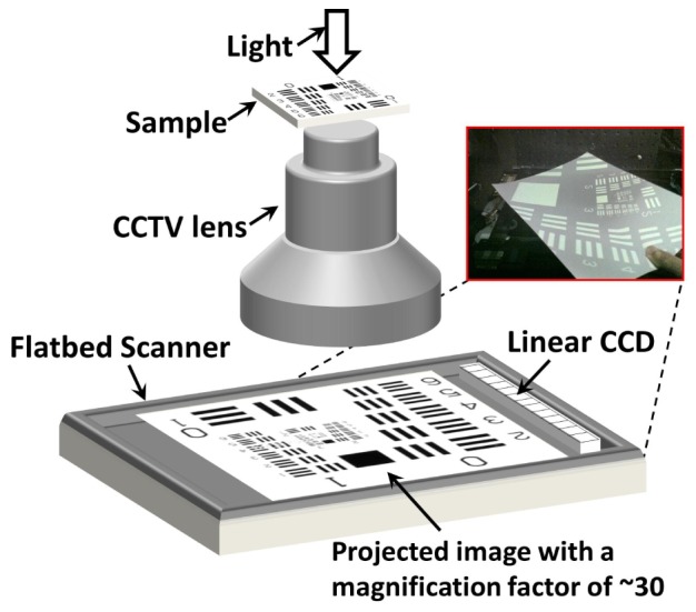
Setup of the 0.5 gigapixel microscopy system (not to scale). A CCTV lens was used to magnify the sample by a factor of 30 and a scanner was used to capture the projected image. The distance between the sample and the CCTV lens is about 1 cm and the distance between scanner and the lens is about 30 cm. Inset on the top right shows the magnified image of a USAF target on a letter size paper held in front of the scanner.
The scanning resolution was set to 2400 dpi (dots per inch) and the FOV of the scanner was set to the maximum scanning area (297 mm × 216 mm). The magnification factor was approximately 30 in our platform, corresponding to a FOV of 10 mm × 7.5 mm and a pixel size of 0.34 µm at the object plane. We used a diffuse LED light source from the top for illumination. Based on these settings, the captured image contained 26400 pixels × 20400 pixels, and thus the setup produced a 0.5 gigapixel pixel image of the sample.
3. Automatic focusing scheme
In a conventional microscope setup, the recording device projects a real time image of the object; therefore, it is relatively easy to manually adjust the stage to the position of best focus. Due to the relatively long acquisition time of the scanner, the sample focusing scheme of the reported platform is not as straightforward as conventional microscope setups. To address this issue, we used an automatic sample focusing scheme with a linear stage, as shown in the inset of Fig. 2 (a2). This focusing scheme consists of three steps: 1) move the stage with a constant speed (5 µm/s); 2) acquire the image at the same time (only certain part of the image is in-focus along the scanning direction); 3) define an F (stands for ‘focus’) index to identify the position of best focus from the acquired image. The F index is a measurement of the sharpness of the image, defined as follows:
| (1) |
where f(x,y) denotes the acquired image, and x, y are the corresponding spatial coordinates.
Fig. 2.
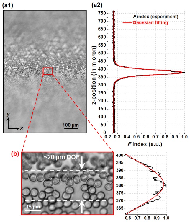
The automatic focusing scheme of the setup. (a1) The acquired image of a blood smear with the stage moving at a constant speed in the z-direction. (a2) Based on the motion speed, we can plot the F index with respect to different z positions, and thus automatically locate the position of best focus. (b) The magnified image of (a), where the depth-of-focus is estimated to be ~20 µm. In this experiment, a diffused green LED (530 nm central wavelength with ~20 nm spectrum bandwidth) was used for illumination.
Figure 2(a1) shows the acquired image of a blood smear following the above steps (only a small portion of the image is acquired for faster scanning). The sample is out-of-focus at the beginning, and the stage brings the sample into focus at the middle part, and finally, the sample is out-of-focus again. Based on the speed of the linear stage, we can plot the F index (with ‘step’ = 2 in Eq. (1)) versus different z-positions, as shown in Fig. 2(a2). The peak of the F index is estimated at z = 381 µm from the Gaussian fit. The magnified image and the corresponding F index are shown in Fig. 2(b), where the depth-of-focus (DOF) is estimated to be ~20 µm. The automatic focusing scheme works well with biological samples and pathology slides. The entire focusing process takes about 1~2 minutes for the reported platform. However, we note that, if the sample is extremely sparse (for example, one small hole on a metal mask), such a scheme would not work and we have to take multiple images at different z positions to find the position of best focus.
4. Resolution and the field curve of the platform
We next characterized the resolution and the field-curve of the reported imaging system. In Fig. 3 , we used a USAF target for resolution characterization. In this experiment, we translated the USAF target across the FOV of the CCTV lens and captured the corresponding images in Fig. 3(a)-3(c). A diffused green LED light source (530 nm central wavelength with ~20 nm spectrum bandwidth) was used as illumination source.
Fig. 3.
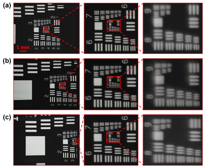
USAF resolution target acquired by the reported microscopy system. The effective FOV is about 10 mm × 7.5 mm, with 26400 pixels × 20400 pixels across the entire image. The imaging performance at the (a) center, (b) 50% away from center and (c) 95% away from center. The line widths of group 9, element 1, 2 and 3 are 0.98 µm, 0.87 µm, and 0.78 µm, respectively.
The imaging performance at the center of the FOV is shown in Fig. 3(a), where the feature at group 9, element 3 (0.78 µm line width) is clearly resolved. In Fig. 3(b) and 3(c), we translate the sample to 50% and 95% of the FOV away from center (100% corresponds to 10 mm), respectively. In both cases, we can still resolve the fine feature at group 9, element 3. This establishes the resolution of our prototype system under the quasi-monochromatic 530 nm illumination, as 0.78 µm over the entire FOV. We note that, by the Nyquist theorem, at least two pixels are needed to capture the smallest detail of the image, and thus, the effective pixel size at the object plane should be less than 0.39 µm (0.78 µm divided by 2). As discussed in Section 2, the image pixel size of the reported platform is 0.34 µm (10 µm scanner pixel size divided by the magnification factor), and thus in accordance with the Nyquist sampling requirement. In Fig. 3(c), the horizontal resolution is less than the vertical resolution. Such an effect is due to the off-axis aberrations of the CCTV lens, such as astigmatism and coma [20]. We also note that, due to the pixel-response variation, line-artifact is present in the raw scanning data [19]. This artifact can be eliminated by performing a simple normalization process: 1) capture a reference image without any sample; 2) normalize the raw scanning image of the sample with the reference image. In this process, the reference image is sample-independent, i.e., it can be used for any sample.
In the second experiment, we characterized the field curve of the imaging system. Our sample was a chrome mask (1.8 cm × 1.8 cm) with a hole-array on it (fabricated by lithography). The holes were about 1 µm in diameter and periodicity of the hole-array was 30 μm. First, we captured a series of images as the chrome mask was mechanically shifted into different z positions. We then analyzed the spot size to locate the best focal plane for different FOVs, with the result shown in Fig. 4 (for example, at 50% FOV, the best focal plane locates at z = 6 µm). The displacement of the best focal plane is directly related to field curve of the imaging system. Remarkably, the result shows that the field curvature is relatively small (maximum observed of ~12 µm z-displacement) over the entire FOV.
Fig. 4.
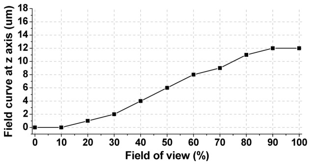
Displacement of the best focal plane of different FOVs (from center to edge FOV). In this figure, 100% in x-axis corresponds to 10 mm.
5. Imaging of a blood smear and pathology slide
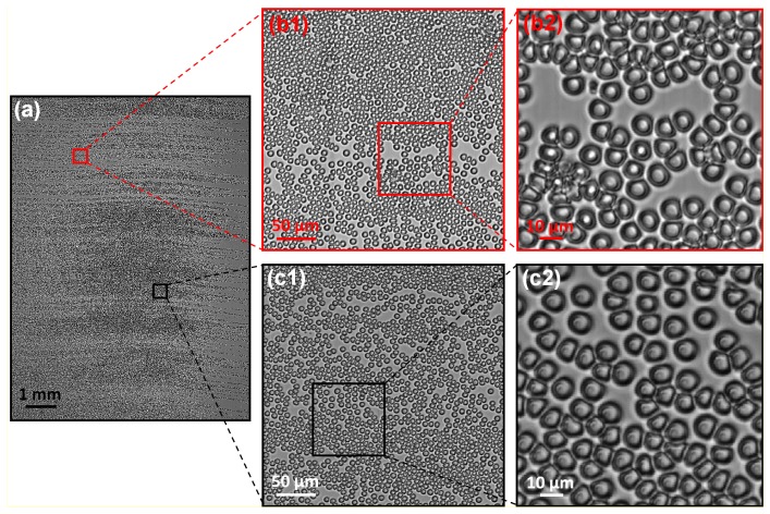
We next used our system for imaging demonstration. First, we acquired a monochromatic image of a human blood smear using a green LED light source. The sample was automatically focused using the automatic focusing scheme described in Section. 2. Figure 5 shows the acquired image, where the scanner and magnification setting is the same as before. We note that there is a 100 fold difference in the scale bars between Fig. 5(a) and 5(b2).
Fig. 5.
Monochromatic image (0.5 gigapixels) of a blood smear. (a) The full frame of the captured image. (b1), (b2) and (c1), (c2) are the expanded view of (a).
6. Conclusion
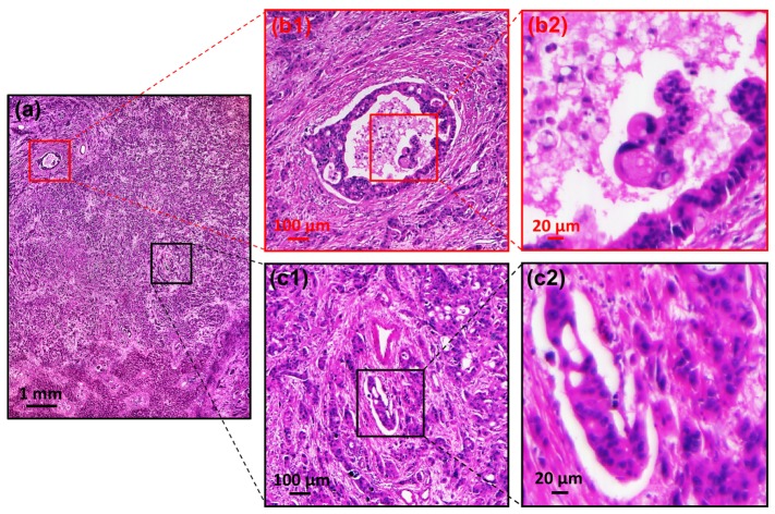
In summary, we report a wide-FOV (10 mm × 7.5 mm) microscopy system which can generate a 0.5 gigapixel image (Fig. 6 ) with 0.78 µm resolution across the entire FOV. We note that there are other large-format professional camera lenses for even larger FOV (for example, 35 mm in diameter). Lenses from the photography/industry community may provide a potential solution for high-throughput microscopy imaging. Interested readers can choose their lenses based on the balance between price and performance.
Fig. 6.
Color image (0.5 gigapixels) of a pathology slide (human metastatic carcinoma in the liver). (a) The full frame of the acquired image. (b1), (b2) and (c1), (c2) are the expanded view of (a).
It is interesting to contrast the SBP and resolution of our demonstrated system to those of the conventional microscope. As shown in Fig. 7 , the effective SBP of our system is more than one order of magnitude greater than the microscope objectives. Compared to typical 10 × and 4 × objectives, our system has both superior SBP and resolution.
Fig. 7.
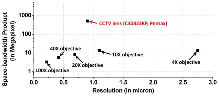
The SBP-resolution summary for microscope objectives and our current CCTV lens based system.
One important limitation of the system is the scanning speed. A full-scan at 2400 dpi scanning resolution took about 10 minutes, limited by the data transfer rate of the USB 2.0 link. There are three strategies to address this issue: 1) use other high speed scanners with faster data links; 2) use multiple scanners for parallelization (we can take out the linear CCDs and its housing components from multiple scanners and assemble them into one scanner); 3) use other scanning devices such as the digital scanning back (for example, a commercially available digital scanning back takes 29 seconds to capture a 0.312 gigapixel image [21]).
More broadly speaking, we believe that this approach can potentially be applied to address whole slide imaging (WSI) in a cost-competitive fashion. To do so, the effective SBP of this approach would have to improve by about an order of magnitude and the resolution should ideally move towards 0.5 microns or better. As the results of this study indicate, an optical lens system with SBP that is substantially greater than those of standard microscope objectives is practical and already exists – by steering away from microscopy standardization restrictions, the available parameter space can afford and support higher SBP. We hope that this work will motivate optical system designers to create systems with even higher SBP and better resolution. As to the challenge of an imaging platform for supporting high SBP, it would be straightforward to implement similar flatbed scanner strategies with longer linear scanning array to provide the requisite imaging pixel count support.
Acknowledgments
We acknowledge the funding support from the United States Department of Defense under grant W81XWH-09-1-0051. The scheme of this work was first presented at CLEO 2012 [22].
References and links
- 1.Oheim M., “Advances and challenges in high-throughput microscopy for live-cell subcellular imaging,” Expert Opin Drug Discov 6(12), 1299–1315 (2011). 10.1517/17460441.2011.637105 [DOI] [PubMed] [Google Scholar]
- 2.Lohmann A. W., Dorsch R. G., Mendlovic D., Zalevsky Z., Ferreira C., “Space-bandwidth product of optical signals and systems,” J. Opt. Soc. Am. A 13(3), 470–473 (1996). 10.1364/JOSAA.13.000470 [DOI] [Google Scholar]
- 3.Gilbertson J. R., Ho J., Anthony L., Jukic D. M., Yagi Y., Parwani A. V., “Primary histologic diagnosis using automated whole slide imaging: a validation study,” BMC Clin. Pathol. 6(1), 4 (2006). 10.1186/1472-6890-6-4 [DOI] [PMC free article] [PubMed] [Google Scholar]
- 4.Dmetrix, “http://www.dmetrix.net/techtutorial1.shtml
- 5.Zheng G., Lee S. A., Antebi Y., Elowitz M. B., Yang C., “The ePetri dish, an on-chip cell imaging platform based on subpixel perspective sweeping microscopy (SPSM),” Proc. Natl. Acad. Sci. U.S.A. 108(41), 16889–16894 (2011). 10.1073/pnas.1110681108 [DOI] [PMC free article] [PubMed] [Google Scholar]
- 6.Lee S. A., Zheng G., Mukherjee N., Yang C., “On-chip continuous monitoring of motile microorganisms on an ePetri platform,” Lab Chip 12(13), 2385–2390 (2012). 10.1039/c2lc40090a [DOI] [PMC free article] [PubMed] [Google Scholar]
- 7.Bishara W., Su T. W., Coskun A. F., Ozcan A., “Lensfree on-chip microscopy over a wide field-of-view using pixel super-resolution,” Opt. Express 18(11), 11181–11191 (2010). 10.1364/OE.18.011181 [DOI] [PMC free article] [PubMed] [Google Scholar]
- 8.Greenbaum A., Luo W., Khademhosseinieh B., Su T.-W., Coskun A. F., Ozcan A., “Increased space-bandwidth product in pixel super-resolved lensfree on-chip microscopy,” Sci. Rep. 3, 1717 (2013). 23611876 [Google Scholar]
- 9.McLeod E., Luo W., Mudanyali O., Greenbaum A., Ozcan A., “Toward giga-pixel nanoscopy on a chip: a computational wide-field look at the nano-scale without the use of lenses,” Lab Chip 13(11), 2028–2035 (2013). 10.1039/c3lc50222h [DOI] [PMC free article] [PubMed] [Google Scholar]
- 10.Wu J., Cui X., Zheng G., Wang Y. M., Lee L. M., Yang C., “Wide field-of-view microscope based on holographic focus grid illumination,” Opt. Lett. 35(13), 2188–2190 (2010). 10.1364/OL.35.002188 [DOI] [PubMed] [Google Scholar]
- 11.Wu J., Zheng G., Li Z., Yang C., “Focal plane tuning in wide-field-of-view microscope with Talbot pattern illumination,” Opt. Lett. 36(12), 2179–2181 (2011). 10.1364/OL.36.002179 [DOI] [PubMed] [Google Scholar]
- 12.Pang S., Han C., Erath J., Rodriguez A., Yang C., “Wide field-of-view Talbot grid-based microscopy for multicolor fluorescence imaging,” Opt. Express 21(12), 14555–14565 (2013). 10.1364/OE.21.014555 [DOI] [PMC free article] [PubMed] [Google Scholar]
- 13.Di J., Zhao J., Jiang H., Zhang P., Fan Q., Sun W., “High resolution digital holographic microscopy with a wide field of view based on a synthetic aperture technique and use of linear CCD scanning,” Appl. Opt. 47(30), 5654–5659 (2008). 10.1364/AO.47.005654 [DOI] [PubMed] [Google Scholar]
- 14.Lee M., Yaglidere O., Ozcan A., “Field-portable reflection and transmission microscopy based on lensless holography,” Biomed. Opt. Express 2(9), 2721–2730 (2011). 10.1364/BOE.2.002721 [DOI] [PMC free article] [PubMed] [Google Scholar]
- 15.Zheng G., Horstmeyer R., Yang C., “Wide-field, high-resolution Fourier ptychographic microscopy,” Nat. Photonics 7(9), 739–745 (2013). 10.1038/nphoton.2013.187 [DOI] [PMC free article] [PubMed] [Google Scholar]
- 16.Ou X., Horstmeyer R., Yang C., Zheng G., “Quantitative phase imaging via Fourier ptychographic microscopy,” Opt. Lett. 38, 4845–4848 (2013). [DOI] [PMC free article] [PubMed] [Google Scholar]
- 17.K. Fife, A. Gamal, and H. Wong, “A 3mpixel multi-aperture image sensor with 0.7 um pixels in 0.11 um cmos,” in IEEE ISSCC Digest of Technical Papers 48–49 (2008). [Google Scholar]
- 18.Ben-Ezra M., “A digital gigapixel large-format tile-scan camera,” IEEE Comput. Graph. Appl. 31(1), 49–61 (2011). 10.1109/MCG.2011.1 [DOI] [PubMed] [Google Scholar]
- 19.Wang S., Heidrich W., “The Design of an Inexpensive Very High Resolution Scan Camera System,” Comput. Graph. Forum 23(3), 441–450 (2004). 10.1111/j.1467-8659.2004.00775.x [DOI] [Google Scholar]
- 20.Zheng G., Ou X., Horstmeyer R., Yang C., “Characterization of spatially varying aberrations for wide field-of-view microscopy,” Opt. Express 21(13), 15131–15143 (2013). 10.1364/OE.21.015131 [DOI] [PMC free article] [PubMed] [Google Scholar]
- 21.http://www.linhofstudio.com/products/cameras/anagramm_digital_reproduction/anagramm_digital_reproduction.html.”
- 22.G. Zheng, X. Ou, and C. Yang, “Towards Giga-pixel Microscopy,” in Conference on Lasers and Electro-Optics 2012, OSA Technical Digest (online) (Optical Society of America, 2012), CTu3J.1. 10.1364/CLEO_SI.2012.CTu3J.1 [DOI] [Google Scholar]


