Abstract
This study examined the performance and photo-bias stability of double-channel ZnSnO/InZnO (ZTO/IZO) thin-film transistors. The field-effect mobility (μFE) and photo-bias stability of the double-channel device were improved by increasing the thickness of the front IZO film (tint) compared to the single-ZTO-channel device. A high-mobility (approximately 32.3 cm2/Vs) ZTO/IZO transistor with excellent photo-bias stability was obtained from Sn doping of the front IZO layer. First-principles calculations revealed an increase in the formation energy of O vacancy defects in the Sn-doped IZO layer compared to the IZO layer. This observation suggests that the superior photo-bias stability of the double-channel device is due to the effect of Sn doping during thermal annealing. However, these improvements were observed only when tint was less than the critical thickness. The rationale for this observation is also discussed based on the oxygen vacancy defect model.
Metal oxide thin-film transistors (TFTs) have attracted considerable attention for applications in the active-matrix (AM) backplanes of liquid crystal displays (LCDs) and organic light-emitting diode (OLED) displays due to their high mobility, low production cost, and low-temperature processing capability1,2,3,4. Despite these advantages, the high instability of metal oxide TFTs to photo bias is a critical issue that must be resolved to implement such TFTs in applications. Accordingly, the degradation mechanism of negative-bias illumination stress (NBIS)-induced instability has been studied extensively. Three NBIS degradation mechanisms have been suggested, including photo-created hole trapping5, photo-ionization of oxygen vacancy defects6,7, and ambient interactions8. The improvement in the NBIS stability of metal oxide TFTs has been achieved based on an understanding of these degradation mechanisms.
High-quality gate insulators, such as SiO2 or Al2O3, which were deposited by plasma-enhanced chemical vapor deposition (PECVD) or atomic layer deposition, were reported to effectively suppress the NBIS instability of the resulting metal oxide TFTs. This suppression was attributed to the large hole injection barrier (>2.0 eV) and low interfacial trap density of these insulators9. Dynamic interactions between the oxide channel and ambient gases, such as oxygen or moisture, can be prevented by choosing the appropriate passivation layer on the back channel10. The photo-ionization of existing oxygen vacancy (VO) defects is related to the intrinsic nature of metal oxide semiconductor materials. The incorporation of carrier suppressors, such as Zr, Hf, and Ga, to the relevant metal oxide semiconductor can help reduce the NBIS instability because these suppressors can effectively reduce the concentration of VO defects in the resulting channel layer. However, the field-effect mobility of the resulting oxide TFTs was adversely affected by the addition of such suppressors11,12.
The incorporation of In cations to multi-component ZnO-based channels is one of best ways to enhance the field-effect mobility of the resulting oxide TFTs4. Unfortunately, increasing the In fraction accelerates the deterioration of NBIS instability of the metal oxide TFTs13 due to the higher rate of formation of VO defects under In-rich conditions14. Consequently, the trade-off relationship between mobility and photo-bias stability in a single channel makes it difficult to produce oxide TFTs with both good bias stability and high field-effect mobility. As an alternative approach, a double-channel structure can provide a solution to the adverse tradeoff between field-effect mobility and photo-bias stability.
Several studies have assessed the benefits of a double-channel structure15,16,17,18,19. Chong et al. reported the insertion effect of Ga-doped ZnO (GZO) at the interface between IGZO and the SiO2 gate insulator on the mobility and positive-bias stress (PBS) instability of the resulting oxide TFTs. The improvement of both the mobility and PBS stability of IGZO/GZO TFTs was attributed to the localization effect of the conducting channel path, where the inserted conducting GZO layer reduced the screening length of the channel layer under an on-state current condition while suppressing the trap-induced PBS instability at the channel bulk and back surface region17. Kim et al. reported the density-of-states (DOS)-based design of the double-channel device18. The optimized HIZO/IZO TFTs exhibited improvement in both the field-effect mobility and NBIS stability compared to those of the single-channel devices. The authors also reported the superior mobility and gate bias stability of ZTO/ITO double-channel devices19. Nevertheless, these studies did not provide an in-depth theoretical explanation of the improvements.
In this study, double-channel oxide TFTs consisting of a back-layer ZTO film and front-layer IZO film were fabricated. The thickness-dependent performance and stability of the front IZO layer were examined experimentally. The optimum device was achieved for the 5-nm-thick IZO device, which exhibited a high field-effect mobility (μFE) of 32.3 cm2/Vs, a low subthreshold gate swing (SS) of 0.12 V/decade, a reasonable threshold voltage (Vth) of 0.5 V, a high Ion/off ratio of > 108, and the best NBIS stability. A depth profile analysis of the channel stack revealed the inter-diffusion of Sn and In atoms, which occurs during thermal annealing at 500°C. Therefore, the front IZO layer was doped with Sn cations. The microscopic origin for such improvement was examined by first-principles calculations based on density functional theory. The formation energy of oxygen vacancies for the IZO front layer substantially increased (by approximately 0.3 eV) due to Sn doping, which is responsible for the improvement in the NBIS stability of the double-channel device.
Results
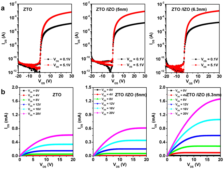
Figure 1a presents the transfer characteristics of the ZTO (control), ZTO/IZO (tint = 5.0 nm), and ZTO/IZO (tint = 6.3 nm) devices. μFE was determined by the maximum trans-conductance at a drain voltage (VDS) of 0.1 V, and Vth was determined from the gate voltage (VGS) required to produce a drain current of L/W × 10 nA at VDS = 5.1 V. The subthreshold gate swing (SS = dVGS/dlogIDS) was extracted from the linear portion of a plot of the log IDS versus VGS. For the first-series devices, the front IZO layer was prepared at an oxygen ratio ([O2]/[Ar + O2]) of 0.3. The single ZTO control device exhibited a μFE, SS, Vth, and Ion/off ratio of 28.8 cm2/Vs, 0.20 V/decade, 1.4 V, and 1.5 × 10⁸, respectively. The transporting properties of the double-channel devices were improved substantially by increasing the thickness of the front IZO layer, as summarized in Supplementary Table S1. Therefore, the high μFE value obtained from the ZTO/IZO (tint = 6.3 nm) devices was 33.0 cm2/Vs. The enhanced transporting properties of the double-channel device were reflected in the superior output characteristics, as shown in Figure 1b. In contrast, the Vth of the double-channel devices were displaced to the negative direction with increasing tint. This result indicates that the number of free electron carriers (Nd) in the channel layer is proportional to the thickness of the front IZO layer. The high mobility of the double-channel devices was attributed to the increasing In content caused by the intercalation of In atoms with a larger radius1,4. In terms of Vth, the ZTO/IZO (tint = 5.0 nm) device was found to be optimal: a low voltage of 0.41 V is desirable for low-power-consumption AM panels. A similar behavior was observed at a higher oxygen ratio ([O2]/[Ar + O2]) of 0.4, as listed in Supplementary Table S1.
Figure 1. Representative transistor performance of the ZTO control device and ZTO/IZO devices.
(a) Transfer characteristics of the ZTO control device, ZTO/IZO (5 nm) device, and ZTO/IZO (6.3 nm) device. The ratio of [O2]/([Ar] + [O2]) was fixed to 0.3 during deposition of the front IZO layer. (b) The corresponding output characteristics of the ZTO control device, ZTO/IZO (5 nm) device, and ZTO/IZO (6.3 nm) device.
The SS value of a given TFT device is related to the interfacial trap density (Dit,max) according to the following equation20:
 |
where kB is Boltzmann's constant, T is the absolute temperature, q is the electron charge, and Ci is the gate capacitance per unit area. The Dit,max of the resulting devices decreased as tint was increased for an oxygen ratio of 0.3 and 0.4, respectively. This increase strongly suggests that the interfacial properties between the SiO2 gate insulator and oxide semiconductor channel layer were improved by inserting a front IZO layer. The physical implication will be discussed later in conjunction with the tint-dependent bias and photo-bias stability.
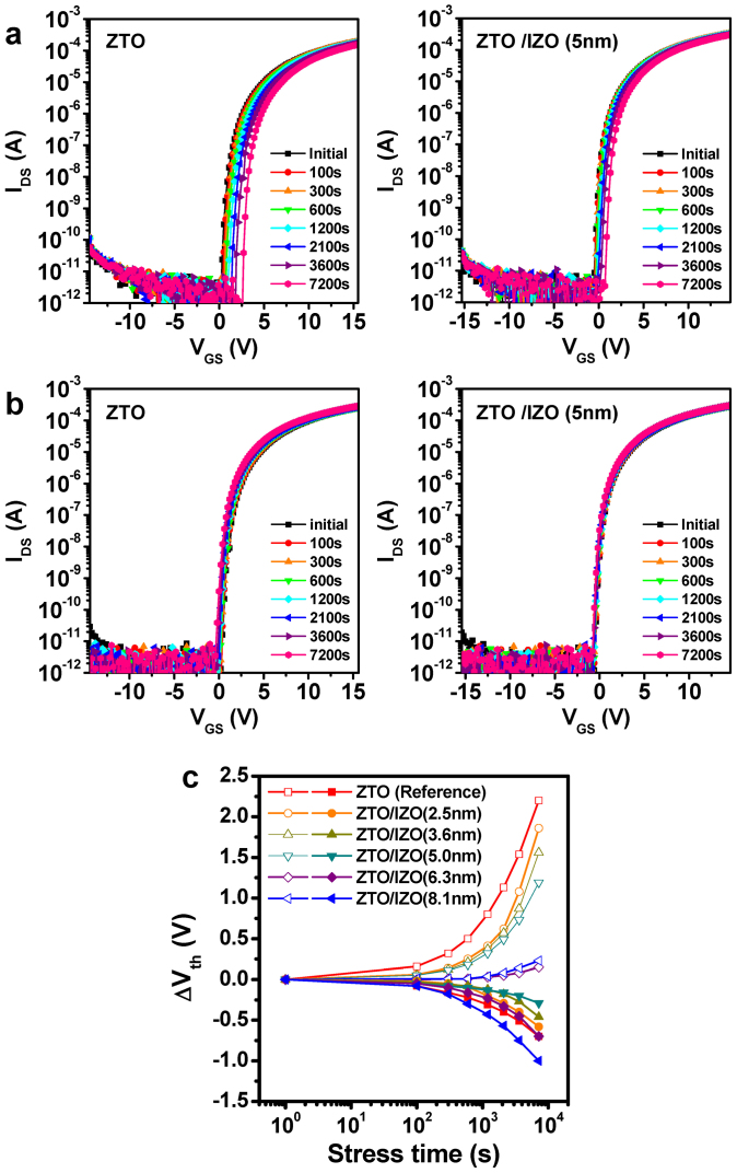
The effects of the PBS and negative gate bias stress (NBS) on the transfer characteristics of both devices were investigated. Figure 2a presents the evolution of the transfer curve as a function of the applied PBS time for the control and ZTO/IZO (tint = 5.0 nm) devices. The devices were stressed under the following conditions: VGS and VDS were set to 20 V and 5.1 V, respectively, at room temperature, and the stress duration was 7,200 s. For the control device, a parallel Vth shift of 2.2 V to a higher voltage with increasing PBS time was observed without an accompanying change in μFE, SS, and the Ion/off ratio. The Vth stability of the IGZO TFTs under PBS was clearly improved by adopting a double-channel structure (see Fig. 2a). It is noted that a Vth shift was further suppressed to ~0.2 V for ZTO/IZO (tint = 6.3 and 8.3 nm) devices.
Figure 2. Gate bias stress stability of the ZTO control device and ZTO/IZO device.
(a) Evolution of the transfer characteristics of the ZTO control device and ZTO/IZO (5 nm) device with increasing PBS time. (b) The variation of the transfer characteristics for the ZTO control device and ZTO/IZO (5 nm) device as a function of the NBS time. (c) Change in Vth for various devices. Empty and filled symbols denote the PBS- and NBS-induced variations, respectively.
The effect of the channel structure on the NBS instability of the resulting TFTs was also investigated. The devices were stressed under a VGS of −20 V and a stress duration of 7,200 s. Again, the NBS-induced variation was reduced significantly from −0.7 V (control device) to −0.3 V for the double-channel device, as shown in Figure 2b. Figure 2c presents the PBS- and NBS-induced Vth variations of the ZTO/IZO devices prepared at an oxygen ratio of 0.3. The PBS-induced Vth displacement decreased significantly with increasing tint suggesting that the front IZO film provides a rapid carrier path and lower effective trap density. The Vth instability by the application of NBS was also suppressed by increasing tint, except for tint ≥ 6.3 nm.
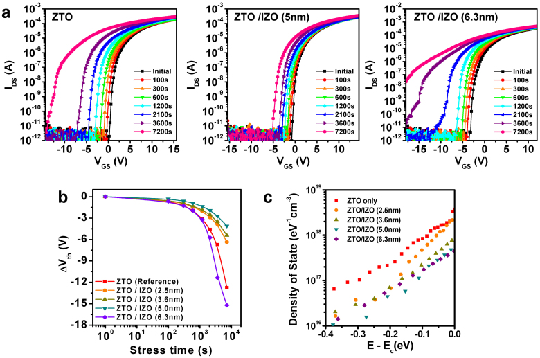
The photo-bias instability of the ZTO and ZTO/IZO devices was compared, as shown in Figure 3a. A green LED light source with a photo intensity of 0.27 mW/cm2 was used under identical NBS conditions. Although the NBIS instability for each device was worse than the dark NBS instability, the changes in Vth by the application of NBIS were similar to those by NBS. When tint was less than the critical thickness (tcrit), the NBIS stability of the double-channel device improved with increasing tint. Here, tcrit is defined as the maximum thickness that results in higher mobility and better photo-bias stability compared to the single-channel device. For example, the negative Vth shift of the double-channel device (tint = 5 nm) was reduced from 12.5 V (single ZTO device) to 4.1 V (see Fig. 3a). The double-channel structure (tint ≤ tcrit) exhibited superior photo-bias stability, and the resulting oxide TFTs exhibited improved transporting properties compared to the control device. This result is difficult to understand because higher-In-containing oxide TFTs suffer from severe NBIS degradation due to the easy formation of oxygen vacancy defect centers. However, when tint > tcrit, the NBIS stability as well as NBS stability of the resulting double-channel device deteriorated abruptly. Therefore, the 6.3-nm-thick device fabricated at an oxygen ratio of 0.3 suffered from the most severe degradation (ΔVth = −15.2 V), which is larger than that of the ZTO control device, as shown in Figures 3a and b.
Figure 3. Photo-bias stability of the ZTO control device and ZTO/IZO device.
(a) Time evolutions of the transfer characteristics for the ZTO control device, ZTO/IZO (5 nm) device, and ZTO/IZO (6.3 nm) device under NBIS conditions. (b) Variation of Vth shift under NBIS conditions for various devices. (c) Calculated DOS distribution as a function of the energy (E – EC) for the devices examined.
To obtain more insight into these anomalous behaviors, the DOS distributions of the devices in this study were calculated using the Meyer-Neldel rule21. Figure 3c presents the DOS distribution as a function of the energy for the single- and double-channel devices. The overall DOS distribution of the double-channel device (tint = 5 nm) was much lower than that of the single-channel device. Here, the extracted DOS distributions are the summation of the bulk trap states (NSS) in the channel region and Nit at the channel/gate insulator interface. Because the thickness of the back ZTO channel was fixed to 35 nm for all devices, the NSS values for both devices would be comparable. Therefore, the In-rich composition can effectively eliminate the Nit at the IZO/gate insulator interface compared to those at the ZTO/gate insulator interface, which is consistent with the Nit,max variations extracted from the SS values.
The PBS instability can be understood based on the carrier trapping mechanism. The amount of charge trapped into the channel bulk and at the channel/insulator interface will be proportional to the number of trap states regardless of the charge polarity. Therefore, the improvement in the PBS stability of the double structure devices can be attributed to the effective decrease in the interfacial trap density compared to that of the single-channel device. This inverse proportionality between the gate bias instability and DOS distribution was observed for all tint values. The MNR-derived DOS energy range was limited from the conduction band edge (EC) to (EC −0.4 eV), which corresponds to the tailing state of acceptor-like traps. Because the quasi-Fermi energy (EF) at the channel interface is positioned near the EC edge under the PBS condition, this DOS distribution directly affects the PBS instability, as discussed earlier. In contrast, NBS and NBIS instability mainly results from the VO deep state. Therefore, a complete understanding of photo-bias instability requires the comparative characterization of the VO density by X-ray photoelectron spectroscopy (XPS) and the theoretical electron calculation of VO defects.
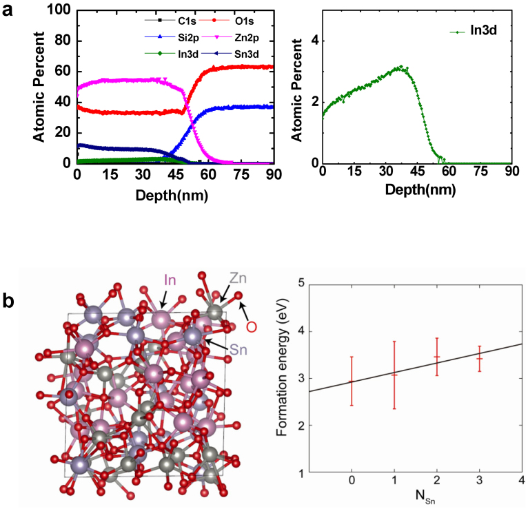
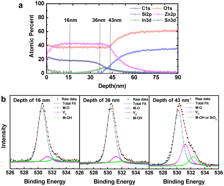
Thus, the atomic distribution and chemical state of a ZTO/IZO film were analyzed by XPS. Figure 4a presents the depth profile of the various elements in the ZTO(35 nm)/IZO(5 nm)/SiO2 stack. The Sn and In atoms in the channel stack region inter-diffused during thermal annealing for 1 h at 500°C, suggesting that the front IZO layer was doped with Sn cations. Pre-existing VO defects in the channel layer have a deleterious effect on the NBIS-induced instability14. This negative effect was attributed to a photo transition from the neutral oxygen vacancy (VO) to the double-charged oxygen vacancy defects (VO+2), which results in the delocalized electrons in the conduction band. The influence of Sn on the Vo formation energy was examined by first-principles calculations using the VIENNA ab initio simulation package (VASP)22 with the similar computational details to those reported in Ref. 23. The projector-augmented wave (PAW) pseudopotentials24 with a kinetic energy cutoff of 500 eV and a 2 × 2 × 2 k-point mesh were used. For the exchange-correlation energy of electrons, the generalized-gradient approximation (GGA) + U calculation was used because it partially corrects the band-gap problem in GGA by decreasing the repulsion between oxygen p and metal d states25. The effective U parameters were set to 7.0, 3.5, and 8.0 eV for the In 4 d, Sn 4 d, and Zn 3 d states, respectively.
Figure 4. Composition analysis of the ZTO/IZO device and electron calculation results.
(a) Depth profile of various elements for the ZTO/IZO(5 nm)/SiO2 stack structure. The enlarged depth profile of In is also shown. (b) Amorphous structure of ITZO, including eight formula units of In2Sn2Zn2O9 and the calculated formation energies of VO as a function of the number of neighboring Sn atoms. The mean values and standard deviation are presented in red, and the black solid line represents a linear regression.
The amorphous structure of the InSnZnO (a-ITZO) compound with a stoichiometry of nIn:nSn:nZn = 1:1:1 was modeled by a first-principles molecular dynamics (MD) simulation. The eight formula units of In2Sn2Zn2O9 were distributed randomly into a cubic supercell. The structure was heated to 2,000 K for 5 ps, and then, the temperature was reduced rapidly to 300 K at a −300 K/ps quenching speed. The lattice parameters and atomic positions were fully relaxed, resulting in the final amorphous structure shown in Figure 4b.
The formation energy (Ef) for VO defects in the neutral state was calculated using the following formula:
 |
where Etot(VO) and  represent the total energy of the supercell with and without VO, respectively, and μO is the chemical potential of oxygen under the given growth condition. In the present study,
  , corresponding to an oxygen-rich limit.
In an amorphous multicomponent oxide, Ef(VO) depends strongly on the local environment of oxygen25. In contrast to the crystal, various types of VO configurations exist in the amorphous structure. Therefore, 33 different VO configurations were calculated by removing an oxygen atom in the modeled a-ITZO and examining how the neighboring cation species affect the formation energy of the VO. In Figure 4b, the formation energies were averaged with respect to the neighboring Sn atoms (NSn). The formation energies increase substantially with increasing NSn, indicating that VO becomes difficult to form as more Sn atoms are introduced to the material. This dependence is consistent with the previous first-principles study that demonstrated the higher formation energy of VO in crystalline SnO2 compared to those of In2O3 and ZnO26.
In addition, a recently proposed model on the peroxide formation through the hole creation inside the valence band may be valid in the present case and may also contribute to the observed photo instability27. By forming O-O bonds, the peroxides increase the carrier density in a manner similar to the oxygen vacancy. The tendency for the peroxide formation may increase as the energy gap is reduced. We theoretically observe that the energy gap of IZO is smaller than that for Sn-doped IZO by approximately 0.3 eV. That is, the formation of photo-induced peroxide is also more significant for IZO. Therefore, the improved NBIS stability for the double-channel devices (tint < tcrit) can be attributed to the suppression of VO defects in the front IZO layer by Sn doping and the reduced Nit density at the front layer/gate insulator interface.
The remaining question is why the thick front channel device (tint > tcrit) suffers from inferior photo-bias stability compared to that of the single-channel device. Figure 5a presents the depth profile of various elements in the ZTO(35 nm)/IZO(8.3 nm) stack at an oxygen ratio of 0.3. The effective diffusion length of Sn atoms was less than the thickness of a front IZO layer. Thus, some portion of the front IZO layer is unaffected by Sn doping during thermal annealing. The existence of an IZO layer with high In content would be responsible for the deterioration of the NBIS stability for a thick front channel device because the formation energy of VO is reduced due to the weak bonding of In and oxygen.
Figure 5. Composition analysis of the ZTO/IZO device.
(a) Depth profile of the elements in the ZTO/IZO(8.3 nm)/SiO2 stack structure. (b) O1s XP spectra of the position at a depth of 16, 36, and 43 nm, which correspond to the bulk ZTO region, near-interfacial ZTO/IZO region, and interfacial IZO/SiO2 region, respectively. The O1s spectra were de-convoluted into three different peaks, the “lattice oxygen peak without oxygen vacancies” (530.4 eV), the “lattice oxygen peak in the oxygen deficient region” (531.2 eV), and the “metal hydroxide peak or SiO2–related peak” (531.3 eV).
Figure 5b shows the evolution of the O1s X-ray photoelectron (XP) spectra along the depth direction. The position at a depth of 16, 36, and 43 nm corresponded to the bulk ZTO region, interfacial ZTO/IZO region, and interfacial IZO/SiO2 region, respectively. The O1s peaks centered at binding energies of 530.4 ± 0.1 and 531.2 ± 0.2 eV arose from oxygen atoms in the oxide lattices without and from oxygen vacancies, respectively, as summarized in Supplementary Table S228,29,30. The peak areas of the oxygen vacancies clearly increased with increasing depth. A larger portion of the increased oxygen vacancies at a depth of 43 nm compared to that at the depth of 36 nm suggests that the front IZO layer consists of a Sn-doped and Sn-free IZO layer. Therefore, the double-channel device with a thick front channel device (tint > tcrit) exhibited poorer NBIS stability due to the large VO concentration of the Sn-free front IZO layer. The extreme case corresponds to the single-IZO-channel device. The oxide TFTs with a 35-nm-thick single IZO channel did not exhibit any Ion/off modulation but instead exhibited simple metallic behavior. The Nd value of the 35-nm-thick IZO film was determined to be > 1020 cm−3 from the Hall effect measurement, which is consistent with the thick IZO film (tint > tcrit) with a high VO concentration.
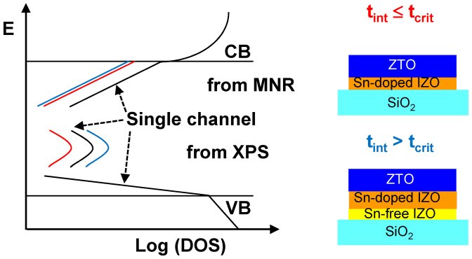
Figure 6 provides a schematic comparison of the total subgap DOS distribution for the ZTO control device and the thin (tint ≤ tcrit) and thick (tint > tcrit) IZO devices. There are two competing factors governing the PBS, NBS, and NBIS instability of the double-channel devices. One factor is the lower Dit,max between the Sn-doped IZO (IZTO) and SiO2 insulator compared to that between the ZTO and SiO2 insulator. The other factor is the creation of VO defects. For thin (tint ≤ tcrit) devices, the suppressed VO defect and lower Dit,max values are responsible for the improvement in the gate bias and photo-bias stability. However, thick (tint > tcrit) devices suffer from the abrupt creation of VO in the interfacial In-rich region due to the limited Sn diffusion to the IZO front layer, which leads to the deterioration of the NBS and NBIS stability.
Figure 6. Proposed subgap DOS distribution.
The black line denotes the acceptor-like tail state and deep VO states of the ZTO control device. The thin (tint ≤ tcrit) and thick (tint > tcrit) IZO devices are represented by the red and blue lines, respectively. The thin IZO double-channel device has fewer interfacial trap states over an entire forbidden bandgap. In addition, the VO formation is strongly suppressed by the Sn-doping effect to the IZO front layer. In contrast, the thick IZO device has extremely deep VO states due to the limited diffusion length of the Sn cation.
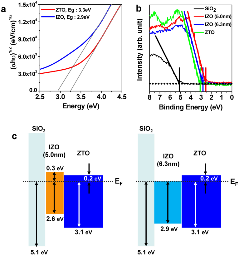
To confirm the proposed origin of the improved mobility and photo-bias stability with the strong tint dependency, the relative band structure for the ZTO/IZO/SiO2 stack was further analyzed by XP spectra using a monochromatic Al-Kα source. The XP valence band (VB) profiles near the bandgap for the ZTO, 5.0-nm-thick IZO, 6.3-nm-thick IZO, and SiO2 are depicted in Figure 7b. The VB maximum of each layer is approximately 3.1, 2.6, 2.9, and 5.1 eV, from the Fermi level for the ZTO, 5.0-nm-thick IZO, 6.3-nm-thick IZO, and SiO2, respectively. The band diagrams obtained from the VB spectra and optical bandgaps of the IZO and ZTO films are depicted in Figure 7c. The 5.0-nm-thick IZO film is in a semiconducting state, whereas the 6.3-nm-thick IZO film is in a degenerated conducting state.
Figure 7. Optical properties and electronic structure of the IZO and ZTO films.
(a) Tauc plot; (αhν)1/2 as a function of the photon energy, hν, where ν is the photon frequency, indicating the optical bandgap (Eg) for the IZO (2.9 eV) and ZTO (3.3 eV) films. (b) XP spectra near the VB maximum of the ZTO, 5.0-nm-thick and 6.3-nm-thick IZO, and SiO2 films. (c) Proposed energy band diagram of the thin and thick IZO double-channel structures based on the obtained VB profile.
This remarkable difference suggests that the thicker IZO film (tint > tcrit) indeed has a high Nd due to the high VO concentration. The tcrit value of the double-channel TFTs clearly depends on the content of VO defect in a front layer. Indeed, the tcrit value for the double-channel TFTs increased from 5.0 to 6.5 nm when the oxygen ratio of O2/[O2 ± Ar] during the sputtering of the IZO layer increased from 0.3 to 0.4, as shown in Supplementary Figure S1. This increase is reasonable because the intentional supply of oxygen species in the IZO front layer slow the abrupt VO formation in the In-rich interfacial region due to the limited diffusion length of the Sn cation. In previous studies, the thickness of the front layer for the optimized double-channel device was in range of 3.5–5.0 nm18,19. These results suggest that the effective diffusion length of the suppressor cations, such as Hf and Sn, into the In-rich front layer (IZO or ITO) during the given thermal annealing is less than 3.5–5.0 nm.
Discussion
Double-channel ZTO/IZO TFTs exhibited improved mobility and photo-bias stability compared to single-channel ZTO TFTs when the front IZO thickness was less than the critical thickness. These intriguing properties were partially attributed to the reduced Dit,max value of the IZTO/SiO2 interface compared to that of the ZTO/SiO2 interface for the ZTO control device. The Sn-doping effect on the front IZO layer is also responsible for the superior photo-bias stability of the double-channel devices because the formation energy of VO defects increased with increasing Sn coordination number. In contrast, the double-channel device with a thick front IZO layer (tint > tcrit) suffered from inferior NBS/NBIS stability and a large negative Vth displacement compared to those of the ZTO control device. This poor performance is attributed to the limited diffusion length of the Sn atoms compared to the thickness of the thick front IZO layer during thermal annealing. Therefore, careful control of the tint for the interfacial layer is essential for designing a double-channel device that exhibits improved performance and bias stability compared to the single-channel device. Overall, double-channel ZTO/IZO TFTs can be used as the backplane electronics for high-resolution and large-sized AMOLED and TFT-LCD displays.
Methods
A 120-nm-thick SiO2 thin film as a gate insulator was deposited onto a patterned Mo (200-nm-thick)/glass substrate by PECVD at 380°C. Front IZO thin films with tint values of 2.5–8.3 nm were deposited onto SiO2/Mo/glass substrates by DC sputtering. The working pressure was 0.26 Pa, and the relative oxygen ratio ([O2]/[Ar + O2]) was varied from 0.30 to 0.40. The DC power density of the InZnO (IZO) target (50 wt% In) was fixed to 2.2 W/cm2, whereas the deposition time was varied from 30 to 240 s. A 35-nm-thick ZTO film (back layer) was deposited onto an IZO/Mo/glass substrate. The oxygen flow rate of [O2]/[Ar + O2] was fixed to 0.10 for all devices. The Zn:Sn composition was approximately 50:50. The active channel was defined using a shadow mask during ZTO/IZO channel formation, and the ITO source/drain (S/D) electrode was deposited using the same sputtering system. The fabricated TFTs had a bottom gate structure with a channel width (W) and length (L) of 1,000 μm and 150 μm, respectively. The devices were annealed in air for 1 h at 500°C. The transfer characteristics of the oxide TFTs were measured using a Keithley 2636 Source Meter at room temperature. The film thickness was determined by ellipsometry and confirmed by X-ray reflectivity measurements. The cation compositions and chemical states of the ZTO and IZO films were examined by X-ray fluorescence spectroscopy (XRF, Themoscientific, ARL Quant'X) and XPS, respectively.
Author Contributions
H.Y.J., J.-U.B. and W.-S.S. designed this work. J.K.J. and S.H. wrote the manuscript. H.Y.J., A.Y.H. and D.-H.K. performed the experiments and electrical measurements. C.K.L. contributed to the XPS analysis. Y.K. and S.H. performed the theoretical calculations. All authors discussed the results and commented on the manuscript. The project was supervised by J.K.J.
Supplementary Material
SI
Acknowledgments
This study was supported by the Industrial Strategic Technology Program funded by MKE/KEIT (10041041), the Basic Science Research Program through the National Research Foundation of Korea funded by the Korean government (NRF-2012R1A2A2A02005854), and the Research Funding from LG Display Company. Y.K. and S.H. were supported by the Pioneer Research Center Program (2012-0009563). The computations were performed at KISTI (No. KSC-2013-C3-011).
References
- Nomura K. et al. Room-temperature fabrication of transparent flexible thin-film transistors using amorphous oxide semiconductors. Nature 432, 488–492 (2004). [DOI] [PubMed] [Google Scholar]
- Kim M. et al. High mobility bottom gate InGaZnO thin film transistors with SiOx etch stopper. Appl. Phys. Lett. 90, 212114 (2007). [Google Scholar]
- Jeong J. K., Chung H.-J., Mo Y. G. & Kim H. D. Comprehensive study on the transport mechanism of amorphous indium-gallium-zinc oxide transistors. J. Electrochem. Soc. 155, H873–877 (2008). [Google Scholar]
- Jeong J. K. et al. High performance thin film transistors with cosputtered amorphous indium gallium zinc oxide channel. Appl. Phys. Lett. 91, 113505 (2007). [Google Scholar]
- Ji K. H. et al. Comparative study on light-induced bias stress instability of IGZO transistors with SiNx and SiO2 Gate Dielectrics. IEEE Electron Device Lett. 31, 1404–1406 (2010). [Google Scholar]
- Chowdhury M. D. H., Migliorato P. & Jang J. Light induced instabilities in amorphous indium-gallium-zinc-oxide thin-film transistors. Appl. Phys. Lett. 97, 173506 (2010). [Google Scholar]
- Ji K. H. et al. Effect of high-pressure oxygen annealing on negative bias illumination stress-induced instability of InGaZnO thin film transistors. Appl. Phys. Lett. 98, 103509 (2011). [Google Scholar]
- Yang S. et al. Suppression in the negative bias illumination instability of Zn-Sn-O transistor using oxygen plasma treatment. Appl. Phys. Lett. 99, 102103 (2011). [Google Scholar]
- Kim J. H., Kim U. K., Chung Y. J. & Hwang C. S. Improvement in the negative bias illumination temperature stress instability of In-Ga-Zn-O thin film transistors using an Al2O3 buffer layer. Physica Status Solidi- Rapid Research Lett. 5, 178–180 (2011). [Google Scholar]
- Jeong J. K. et al. Origin of threshold voltage instability in indium-gallium-zinc oxide thin film transistors. Appl. Phys. Lett. 93, 123508 (2008). [Google Scholar]
- Yang B. S. et al. Role of ZrO2 incorporation in the suppression of negative bias illumination-induced instability in Zn-Sn-O thin film transistors. Appl. Phys. Lett. 98, 122110 (2011). [Google Scholar]
- Kwon J.-Y. et al. Investigation of light-induced bias instability in Hf-In-Zn-O thin film transistors: A cation combinatorial approach. J. Electrochem. Soc. 158, H433–437 (2011). [Google Scholar]
- Kamiya T., Nomura K. & Hosono H. Present status of amorphous In-Ga-Zn-O thin-film transistors. Sci. Technol. Adv. Mater. 11, 044305 (2010). [DOI] [PMC free article] [PubMed] [Google Scholar]
- Ryu B., Noh H.-K., Choi E.-A. & Chang K. J. O-vacancy as the origin of negative bias illumination stress instability in amorphous In-Ga-Zn-O thin film transistors. Appl. Phys. Lett. 97, 022108 (2010). [Google Scholar]
- Kim S. I. et al. High performance oxide thin film transistors with double active layers. in IEDM Tech. Dig. pp. 73–74 (2008). [Google Scholar]
- Park J. C. et al. Highly stable transparent amorphous oxide semiconductor thin-film transistors having double-stacked active layers. Adv. Mater. 22, 5512–5516 (2010). [DOI] [PubMed] [Google Scholar]
- Chong E. et al. Localization effect of a current-path in amorphous In-Ga-Zn-O thin film transistors with a highly doped buried-layer. Thin Solid Films 519, 4347–4350 (2011). [Google Scholar]
- Kim H.-S. et al. Density of states-based design of metal oxide thin-film transistors for high mobility and superior photostability. ACS Appl. Mater. Interfaces 4, 5416–5421 (2012). [DOI] [PubMed] [Google Scholar]
- Kim J.-I. et al. Improvement in both mobility and bias stability of ZnSnO transistors by inserting ultra-thin InSnO layer at the gate insulator/channel interface. Appl. Phys. Lett. 99, 122102 (2011). [Google Scholar]
- Kanichi J. & Martin S. in Thin Film Transistors (Kagan C. Y., & Andry P., (ed.)) 87 (Dekker, New York, 2003). [Google Scholar]
- Ji K. H. et al. The effect of density-of-state on the temperature and gate bias-induced instability of InGaZnO thin film transistors. J. Electrochem. Soc. 157, H983–986 (2010). [Google Scholar]
- Kresse G. & Furthmüller J. Efficient iterative schemes for ab initio total-energy calculations using a plane-wave basis set. Phys. Rev. B 54, 11169 (1996). [DOI] [PubMed] [Google Scholar]
- Kang Y. et al. Microscopic origin of universal quasilinear band structures of transparent conducting oxides. Phys. Rev. Lett. 108, 196404 (2012). [DOI] [PubMed] [Google Scholar]
- Kresse G. & Joubert D. From ultrasoft pseudopotentials to the projector augmented-wave method. Phys. Rev. B 59, 1758 (1999). [Google Scholar]
- Noh H. K. et al. Electronic structure of oxygen-vacancy defects in amorphous In-Ga-Zn-O semiconductors. Phys. Rev. B 84, 115205 (2011). [Google Scholar]
- Ágoston P., Albe K., Nieminen R. M. & Puska M. J. Intrinsic n-type behavior in transparent conducting oxides: A comparative hybrid-functional study of In2O3, SnO2, and ZnO. Phys. Rev. Lett. 103, 245501 (2009). [DOI] [PubMed] [Google Scholar]
- Nahm H.-H., Kim Y.-S. & Kim D. H. Instability of amorphous oxide semiconductors via carrier-mediated structural transition between disorder and peroxide state. Phys. Status Solidi B 249, 1277 (2012). [Google Scholar]
- Fan J. C. C. & Goodenough J. B. X-ray photoemission spectroscopy studies of Sn-doped indium-oxide films. J. Appl. Phys. 48, 3524–3531 (1997). [Google Scholar]
- Ishida T., Kobayashi H. & Nakato Y. Stuructures and properties of electron-beam-evaporated indium tin oxide-films as studied by x-ray photoelectron-spectroscopy and work-function measurements. J. Appl. Phys. 73, 4344–4350 (1993). [Google Scholar]
- Major S., Kumar S., Bhatnagar M. & Chopra K. L. Effect of hydrogen plasma treatment on transparent conducting oxides. Appl. Phys. Lett. 49, 394–396 (1986). [Google Scholar]
Associated Data
This section collects any data citations, data availability statements, or supplementary materials included in this article.
Supplementary Materials
SI


