

Abstract
The electric-voltage-modulated magnetism in multiferroic heterostructures, also known as the converse magnetoelectric (ME) coupling, has drawn increasing research interest recently owing to its great potential applications in future low-power, high-speed electronic and/or spintronic devices, such as magnetic memory and computer logic. In this article, based on combined theoretical analysis and experimental demonstration, we investigate the film size dependence of such converse ME coupling in multiferroic magnetic/ferroelectric heterostructures, as well as exploring the interaction between two relating coupling mechanisms that are the interfacial strain and possibly the charge effects. We also briefly discuss some issues for the next step and describe new device prototypes that can be enabled by this technology.
Keywords: multiferroic heterostructures, size dependence, magnetoelectric, magneto-optical Kerr effect, domain dynamics
1. Introduction
Controlling magnetic anisotropy or magnetization direction in a magnetic material directly by applying an electric-voltage, i.e. the converse magnetoelectric (ME) effect, has become a central issue in the fields of spintronics and multiferroics [1–10]. It can provide a fast and extremely energy-efficient way for modulating magnetism compared with the traditional way of using external magnetic fields or spin currents [11], and has thus tremendous potential in future low-power and high-speed electronic devices, such as the voltage-driven [12–18] or assisted [19–22] magnetic memories, voltage-actuated logic circuits [23,24] and microwave devices [25,26]. Earlier demonstrations of voltage-modulated magnetism include the electric-field manipulation of the Curie temperature Tc [27], the coercive field Hc [28], and the magnetization vector [29] in thin films of low-temperature diluted magnetic semiconductors (DMSs), such as (In, Mn)As and (Ga, Mn)As (4–5 nm). Similar coercivity modulation has been observed in ferromagnetic (FE) FePt or FePd (2 nm) thin films which are immersed in a liquid electrolyte, followed by the clear voltage-induced magnetic anisotropy changes in either ultrathin Fe (0.2–0.9 nm) films sandwiched between MgO and gold [30] or Co40Fe40B20 (0.8–2 nm) films sandwiched between MgO and Ta [31]. Nevertheless, most of these experimental efforts are limited to low temperature (far below room temperature due to the low Tc of DMSs) and/or high electric fields (1 MV m−1 or above).
Alternatively, such electric-voltage modulation of magnetism can be realized by virtue of the coupling ME effect across the interface of multiferroic heterostructures which artificially combines magnetic and piezoelectric/ferroelectric (FE)/ME/multiferroic phases. Approaches include the strain-driven converse ME coupling [5–8], exchange bias [32–40] or interfacial charge-driven ME effects [41–55]. Among them, the strain-driven converse ME effect is normally understood as a product effect [5] of the inverse piezoelectric and/or ferroelastic coupling (electrical/mechanical) in the piezoelectric/FE phase and the magnetoelastic (mechanical/magnetic) coupling in the magnetic phase. For illustration, a phenomenological model has recently been developed to understand such strain modulation in a typical multiferroic magnetic/FE-layered heterostructure [56]. It is found that the magnetic easy axis (i.e. spontaneous magnetization) of the magnetic layer can either be switched from an initial in-plane to an out-of-plane direction, strengthened in a certain direction (becoming easier) or be rotated by 90° in the film plane (figure 1), depending on the signs and magnitudes of both the electromechanical strain applied to the magnetic layer and the magnetostriction constant. Moreover, much theoretical [57–60] and experimental [61–69] efforts have been devoted to understanding the mesoscopic mechanism (e.g. domain evolution and switching dynamics) of such strain-driven converse ME effects as is discussed later in this article.
Figure 1.
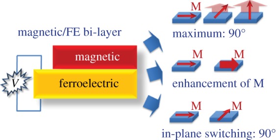
Three different ways of electric-voltage-induced magnetic easy axis (i.e. the spontaneous magnetization M) rotations in a multiferroic magnetic-ferroelectric (FE) bilayer heterostructure.
On the other hand, bias exchange-based ME coupling requires an ME-antiferromagnetic (AFM) phase (e.g. Cr2O3 [32–34]) or FE–AFM (e.g. YMnO3 [35], BiFeO3 [36–39] or LuMnO3 [40]). In these materials, the AFM order can intrinsically be manipulated by external voltages [36], which would allow the further modulation of FM order in the neighbouring FM phase via the exchange coupling [70,71] between the AFM and FM orders.
More recently, it has been reported that the charges at the magnetic-FE interface can also act as a medium that couples electric-voltages towards modulation of magnetism, either through the electrostatic accumulation of spin-polarized charges [41–44] or by purely electronic origins, such as the interfacial orbital hybridization [45–50] and the interfacial orbital reconstruction [51–55] (for details, see comprehensive review [10]). Compared with the strains which can normally be sustained throughout the heterostructure [5–8], such charge-driven ME effects can only occur at the heterointerface ranging from the first few atomic layers to several nanometres (normally less than 10 nm) depending on the charge screening length of a specific magnetic film [9,10]. As a result, such charge effects may become remarkable only when the thickness of the magnetic film and/or the heterostructure becomes small. For example, a butterfly-shaped magnetization-electric field (M–E) at room temperature has been observed in a multiferroic FM/FE heterostructure with an La0.7Sr0.3MnO3 (LSMO, 20–50 nm) thin film grown on rhombohedral Pb(Mg1/3Nb2/3)0.72Ti0.28O3 (PMN-PT), which tracks the butterfly-shaped strain-E loop of PMN-PT, demonstrating a strain-induced converse ME coupling across the LSMO/PMN-PT interface [72]. However, in a similar multiferroic Pb(Zr0.2Ti0.8)O3(PZT, 250 nm)/LSMO film (4 nm) heterostructure, a well-defined square-shaped M–E loop has been observed [73] which is confirmed to be driven by interfacial spin-polarized charges using X-ray absorption near edge spectroscopy [54] later on. Although these are two bit different cases [72,73], this discrepancy would lead to a thickness-dependent voltage-modulated magnetism associated with interaction between strain and charge effects, which is the first question to be explored in this article (§2). On the other hand, the lateral size of the heterostructures would have influences on the voltage-modulated magnetism as well. First, the magnetic films can be in either single- or multi-domain states under different lateral sizes, which could result in different voltage-induced magnetization-switching behaviours. From an application perspective, reducing the lateral size is critical to the device miniaturization. With this regard, lateral size-dependent voltage-modulated magnetism is investigated in §3. The concluding remarks are summarized in §4.
2. Thickness-dependent voltage-modulated magnetism
Here, we first propose a phenomenological model to investigate such thickness-dependent voltage control of magnetization by simultaneously incorporating the strain and charge effects. Then some experimental demonstrations are given.
(a). Phenomenological model
Let us consider a multiferroic FM/FE composite thin film grown on SrTiO3(STO) single-crystal substrate, with BaTiO3(BTO) as the FE layer and SrRuO3(SRO) the bottom electrode. When applying an electric-voltage V across the heterostructure between the top FM thin film and the bottom SRO, the total magnetic free energy of the FM thin film in a single-domain state can be expressed as [74]
| 2.1 |
where Fmc is the magnetocrystalline anisotropy, Fshape the shape anisotropy, Fme the magnetoelastic anisotropy and Fs the surface anisotropy. Influences of the strain-induced coupling and the interface charge-driven coupling are described by the magnetoelastic anisotropy Fme and the surface anisotropy Fs, respectively, both of which can be altered by external voltages, and thus the modulation of the overall magnetic properties. Among them, Fs can be written as [30,75]
| 2.2 |
where m3 refers to the direction cosine, Ks and ΔKs(V) denote the surface anisotropy and its change under external electric-voltage V , and d is the thickness of the FM thin film. These free energy contributions are further transformed into a perpendicular effective anisotropy field HOPeff [74]. The FM thin film would present an out-of-plane easy axis upon a positive HOPeff while a negative HOPeff indicates an in-plane easy axis orientation. Accordingly, the voltage control of magnetization can be related to the voltage-induced change of HOPeff, i.e. ΔHOPeff[=HOPeff(V)/HOPeff(0)−1].
For illustration, figure 2 shows the voltage-induced changes of the HOPeff in (001)-oriented LSMO/BTO multiferroic bilayer films with various thicknesses d of the LSMO films at T=5 K. As the thickness decreases from 30 to 1 nm, the shape of the ΔHOPeff-voltage curve would gradually change from a butterfly-shaped loop (e.g. 30 nm) to a hysteresis square-like one (1 nm), indicating that the dominative ME coupling mechanism would shift from a strain effect to an interface charge-mediated coupling as mentioned above. In particular, there exists a transition thickness dtr for the magnetic thin film where contributions from the charge and strain become equal, which is dependent on the materials parameters [74]. For (001) LSMO, dtr is calculated to be about 4.2 nm. When the film thickness is larger than dtr, the strain effect would play a major part otherwise the charge effect would be dominative. Specifically, the loop of 5 nm shows mixed behaviour of the butterfly-curve and square-loop (figure 2), manifesting itself as an interface-charged and strain-co-mediated ME coupling.
Figure 2.
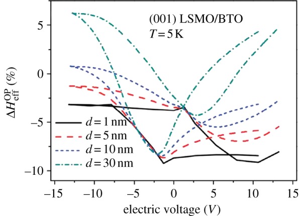
ΔHOPeff (the change of the perpendicular effective magnetic anisotropy field) versus V (electric-voltage) loops in (001) LSMO/BTO multiferroic composite thin film with different thicknesses d of the LSMO thin films. (Adapted from Hu et al. [74].)
(b). Experimental demonstrations
To measure such thickness-dependent converse ME coupling in a multiferroic FM/FE composite thin film, a novel AC-mode electric-field (E)-induced magneto-optical Kerr effect (E-MOKE) method, wherein the Kerr signal is proportional to the magnetization and can be modulated by voltage (V) via ME coupling, was employed herein. Such an AC-mode E-MOKE method can allow an in situ acquisition of the Kerr-V loop (by averaging hundreds of loops) without relying on external magnetic field H, which makes it suitable to be used in multiferroic magnetic/FE composite thin films. Moreover, the desired Kerr-V loops can be obtained within several seconds, which is much faster than the common E-MOKE method using DC voltage bias. Besides, the applied low-frequency voltage can effectively minimize the possible leakage current in the FE thin film and the concomitant side effect from heat. Details about the experimental apparatus are described in [76].
Now let us turn to the characterization of the thickness-dependent voltage-modulated magnetization using such an AC-mode E-MOKE method. The first example is a composite Ni/BTO thin film grown on Nb-doped SrTiO3 (STO) single-crystal substrate, wherein the (001)-oriented epitaxial BTO film is prepared by pulse laser deposition and the polycrystalline Ni film is grown by magnetron sputtering [77]. A typical butterfly-shaped out-of-plane piezostrain loop is obtained using a piezoelectric force microscope (PFM) (figure 3a). Figure 3b shows the obtained Kerr-V loops of the multiferroic Ni/BTO heterostructure with different thicknesses of Ni films, measured by the AC-mode E-MOKE method. Among them, the loop of the 20 nm Ni film exhibits butterfly-shaped behaviour in response to the piezostrain loop, demonstrating a dominative strain-driven ME effect. The loop of 5 nm Ni is linear-like only with a small hysteresis at zero field, which could result from the interface effect [74]. Moreover, the 10 nm loop shows a combined butterfly-shaped and linear characteristic, which might indicate the coexistence of the strain and possible charge effects, and therefore qualitatively agrees with the phenomenological model.
Figure 3.
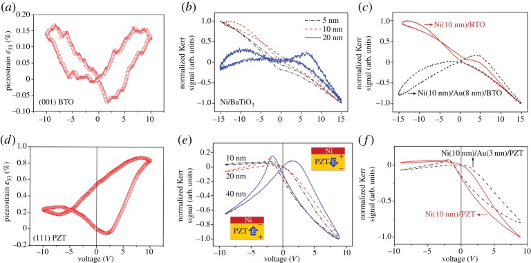
Out-of-plane piezostrain loops of (a) the (001) BTO film and (d) the (111) PZT film. Normalized Kerr signal as a function of voltage in the (b) Ni/BTO and (e) Ni/PZT heterostructures with various thicknesses of the Ni films. The insets show the directions of the polarization and the applied electric-voltage (field). Comparison of the Kerr-V loops in (c) Ni/BTO and Ni/Au/BTO, (f) Ni/PZT and Ni/Au/PZT heterostructures. (Adapted from Shu et al. [77] and Li et al. [78].)
Such coexistence of the strain and interface effects has also been observed in a similar multiferroic Ni/Pb(Zr,Ti)O3 (PZT)/Pt/Si layered structure with various thicknesses of Ni films [78]. Among them, the (111)-textured PZT film exhibits much larger out-of-plane piezostrain ε33 (up to 0.87%) than that of BTO (approx. 0.17%), as shown in figure 3d. As a result, the acquired Kerr-V loops display well-defined butterfly-like patterns even when the thickness of the Ni film decreases to 10 nm (figure 3e), indicating a stronger strain effect in the Ni/PZT layered structure than that in Ni/BTO (figure 3b). Moreover, two distinct and stable magnetization states are observed at zero voltage bias corresponding to the bistable strain states in the piezostrain loop (figure 3d). The latter is induced by the existing polarization state in the as-grown film. Despite such a strong strain effect, the contribution from the possible interfacial charges still cannot be ruled out, because the loop would become more symmetric when the thickness increases (figure 3e).
To further investigate the interaction between these two coupling mechanisms, a thin gold layer (Au, 3–8 nm) with good electrical conductivity was sputtered to separate the Ni from the BTO or PZT layer, and thereby could suppress the possible charge effect occurring at the metal–oxide interface [77,78]. Meanwhile, it would not hamper the effective strain transfer owing to the small thickness and benign bonding property of the Au layers. Their corresponding Kerr-V loops are plotted in figure 3c,f for comparison. As shown, the loop becomes more symmetric and exhibits a butterfly-like characteristic after inserting the gold layer in both the Ni/Au/BTO and the Ni/Au/PZT cases, clearly indicating the suppression of the interface effect. Among them, the thicker 8 nm Au layer sandwiched between the Ni and BTO layers shows a more remarkable change in the loop shape (figure 3c) compared with the 3 nm Au between the Ni and PZT (figure 3f). Such comparison provides evidence for the coexistence and interaction of the strain and possible interfacial charge effects in the multiferroic magnetic/FE heterostructure. Nevertheless, more detailed characterization and analysis on the magnetic/interface are needed.
3. Size-dependent voltage-modulated magnetism by phase-field approach
In addition to the film thickness, the lateral size (i.e. the length and width, assumed to be equal herein) of the magnetic film would also exert significant influence on the domain states as a result of the competing exchange and magnetostatic energy [79,80], for example, the film would display a uniform single-domain structure at small sizes owing to the dominative exchange anisotropy, whereas it would be in a multi-domain state at large sizes in order to reduce the magnetostatic energy. These domain structures would lead to different voltage-induced magnetization-switching characteristics accordingly [57,58], which is critical to the potential device application [59,60]. Here, we use a phase-field model [81–83] to investigate such lateral size-dependent voltage manipulation of magnetization. This computational model is capable of simulating the domain structure evolution process without any a priori assumptions on the possible domain structures, and thus shows better accuracy than thermodynamic calculations [18,56]. It also has advantages over common micromagnetic simulations. The latter typically do not incorporate the elastic energy contribution and the corresponding mechanical boundary condition for a film constrained by a substrate. For simplicity, only the strain effect is considered in the phase-field model.
(a). Out-of-plane magnetization switching by out-of-plane voltage
For illustration, figure 4a shows the isotropic strain-induced out-of-plane magnetization switching in a highly magnetostrictive (001) CoFe2O4 (CFO) film of 64×64×18 nm3 [57]. Such isotropic strain ε0 can be obtained either from the intrinsic lattice and/or thermal mismatch between a film and a substrate [84] or from external piezoelectric actuation [85]. As seen, the CFO film displays a uniform single-domain structure at such a small lateral size (see the inset of figure 4a). The magnetic domain would rotate abruptly from an in-plane direction to an out-of-plane one (e.g. from [−100] to [001]) as the biaxial strain exceeds a critical strain of about 0.01%, corresponding to a first-order thermodynamic phase transition [56]. Figure 4b shows the temporal evolution of the magnetic vectors at the critical strain, illustrating a typical coherent vector rotation process in single-domain magnets [86]. By contrast, a multi-domain 192×192×18 nm3 CFO film exhibits a gradual strain-induced out-of-plane magnetization-switching feature via domain-wall motion or domain nucleation [66,86], as shown in figure 4c. Specifically, the film would present an out-of-plane multi-domain structure with a typical 180° Bloch wall (e.g. see the circle 2 in figure 4d) under a positive in-plane strain ε0 of 0.3%. Note that even local 180° Ising-type-like wall is observed (see the circle 1 in figure 4d) owing to the relative strong elastic energy which can significantly narrow down the domain-wall length [57]. On the other hand, the film would display an in-plane multi-domain structure with a vortex-type 180° Néel wall (see the circle 3 in figure 4d) under a negative ε0 of −0.3%. It is also noteworthy that no matter for the abrupt switching in single-domain magnets or the gradual switching in multi-domain magnets, the film would turn back to the original domain state of zero strain driven by the out-of-plane demagnetization energy if removing the external elastic stimuli.
Figure 4.

Out-of-plane magnetization MOP of (a) single-domain 64×64× 18 nm3 and (c) multi-domain 192×192×18 nm3 (001) CoFe2O4 films of as a function of the isotropic in-plane strain ε0. The insets represent the magnetic domain structures at ε0=±0.3%, with each arrow indicating one specific domain orientation. Vector diagrams for (b) the temporal (N denotes the time step) magnetization evolution of the single-domain film at the critical switching strain of 0.01% and (d) the local magnetization distributions in the multi-domain films with a ε0 of (top) 0.3% and (bottom) −0.3%. The circles denote various types of magnetic domain walls: ‘1′-the Ising-type-like wall; ‘2′–180° out-of-plane Bloch wall; ‘3’–180° in-plane Néel wall. (Colour bar) m3 indicates the normalized magnetization in the [001] direction. (Adapted from Hu et al. [57].)
(b). In-plane magnetization switching by in-plane voltage
The magnetization and/or the magnetic domain can also be rotated by 90° in the film plane upon applying anisotropic in-plane piezostrains [25,26,56]. Consider a (001) CFO film attached to a (001) lead zirconate niobate-lead titanate (PZN-PT) layer with ultrahigh piezoelectric response [87]. An electric-voltage is applied transversely to the (001) PZN-PT layer to produce biaxial in-plane anisotropic piezostrains. For comparison, figure 5 shows the magnetization switching in both the single-domain 64×64×18 nm3 and the multi-domain 192×192×18 nm3 CFO films upon applying a dynamic electric (E)-field with a magnitude of 20 kV m−1 (figure 5a) to the adjacent PZN-PT layer [58]. Among them, the magnetization of the single-domain CFO film can be reversibly switched between the two orthogonal in-plane directions of [010] and [100], which can remain stable even when removing the E-field (figure 5b,d) owing to the potential barrier provided by the strong magnetocrystalline energy of CFO [15]. Such E-induced bistable magnetization states can be used to develop non-volatile memory devices [15,16]. By contrast, the multi-domain 192×192×18 nm3 CFO film would not resume the original magnetization state upon applying a reverse E-field (figure 5c), whereas it would present a very small average magnetization owing to the cancelling of magnetic moments between two degeneration directions despite the locally in-plane 90° switching (see domain structures in sequences 2 and 4 of figure 5e). Moreover, unlike the case in single-domain CFO films, the magnetization state cannot be retained when turning off the electric supply, while it would exhibit typical vortex-type multi-domain structures with in-plane domains (see domain structures in sequences 3 and 5 of figure 5e) driven by the competing exchange and demagnetization anisotropy field.
Figure 5.
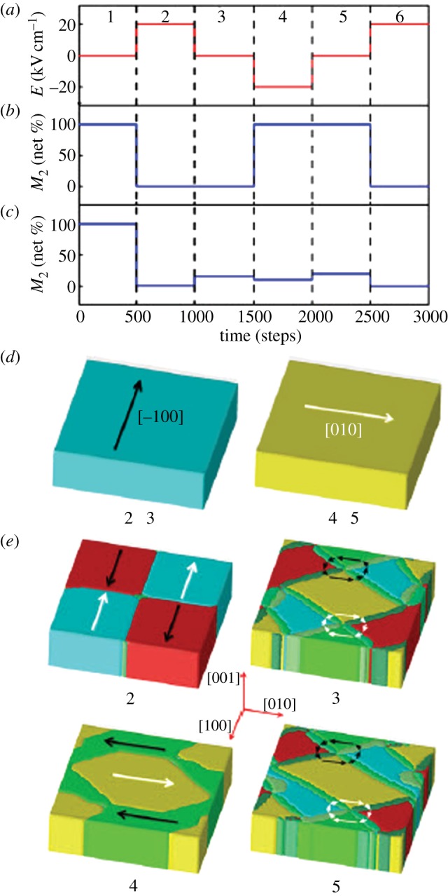
(a) Sequences of the square-wave electric field used for actuation. Corresponding changes of the average magnetization along the [010] crystal direction, i.e. M2(average)=M[010]−M[0−10], in (b) single-domain 64×64× 18 nm3 and (c) multi-domain 192×192×18 nm3 (001) CoFe2O4 films. Typical magnetic domain structures during various electric-field sequences (see the numbers at the bottom) in either (d) the single-domain or (e) multi-domain CoFe2O4 films. The arrows indicate the magnetization directions. (Adapted from Hu et al. [58].)
(c). In-plane magnetization switching by out-of-plane voltage
For non-volatile high-density memory applications, it is highly desirable to achieve non-volatile in-plane magnetization switching by using out-of-plane voltage rather than in-plane voltage. In order to produce biaxial in-plane anisotropic piezo-/ferroelastic strains by longitudinally applying a voltage to the FE layer, we can use a (011) FE layer (or maybe (001) rhombohedral FE layer with spontaneous polarization along 〈111〉 directions). For example, a (011) lead magnesium niobate-lead titanate (PMN-PT) can produce bistable anisotropic in-plane piezostrains [88]. For further illustration, we consider an Ni/PMN-PT heterostructure. The Ni film with robust magnetoelastic coupling [89] has been widely used in electronic devices [90].
As the first example, the thickness-dependent electrical-driven magnetization-switching behaviour in the Ni thin film is shown in figure 6a, wherein bistable magnetization states are displayed at zero voltage bias in response to an almost 90° in-plane magnetization switching as illustrated in figure 6b. Note that a small DC bias magnetic field of 40 Oe is applied to ensure a deterministic and reversible switching back to the initial [010] direction that is preset by annealing the Ni film in a magnetic field. Such bias fields can be easily obtained by employing a pinning or synthetic antiferromagnetic layer [91] in terms of the practical design of voltage-controlled magnetoresistive random access memory (MRAM) devices [59]. As shown in figure 6a, the maximum rotation angle (derived from the direction cosine mx) at E=0 slightly increases by 5° as the thickness of the Ni decreases from 35 to 5 nm. Such an improvement is attributed to the suppression of the out-of-plane magnetization component owing to the enhanced demagnetization in thinner magnetic films, which would in turn facilitate the in-plane magnetization rotation. This may suggest the first design principle for the potential memory device: the thinner, the better. However, growing thinner films would be more technically challenging. Besides, the charge and/or other interface effects could have additional influence on the magnetization switching [74], especially in ultrathin (several monolayers) films [92], but are not considered herein regarding the ultrahigh piezoelectric response of the PMN-PT which would in principle produce a dominative strain-driven ME coupling [74]. Nonetheless, 5 nm could be a well-compromised thickness for the metallic Ni layer grown on PMN-PT based on the results in figure 6. It is also worth noting that the required actuation electric field is ultralow (|E|<0.2 V μm−1), and would thus lead to an ultralow write energy [59].
Figure 6.
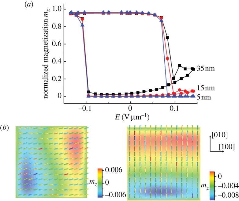
(a) Electric-field-induced magnetization rotation in the Ni films with thicknesses of 35 nm (squares), 15 nm (circles) and 5 nm (triangles), respectively. mx indicates the normalized magnetization in the in-plane [100] direction. The lateral size is taken as 64 nm. (b) Vector diagrams of the bistable magnetization distributions at E=0 in the 64×64× 35 nm3 Ni films. (Colour bar) mz indicates the normalized magnetization in the out-of-plane [001] direction. (Adapted from Hu et al. [59].)
The lateral size-dependent switching behaviour is also discussed (figure 7a) as, in general, a smaller lateral size is good for achieving higher storage capacity, i.e. the smaller, the better. As shown in figure 7b, the film would change from a uniform single-domain to a non-uniform multi-domain structure when the lateral size exceeds 64 nm, similar to the case in CFO films as discussed above. The domain walls in multi-domain states would greatly hamper the switching process, and therefore leads to much smaller magnetization rotation angles (i.e. around 31° (128 nm) and 8° (192 nm) compared with the 75° (64 nm); figure 7a). Nevertheless, the magnetization switching would somewhat be restricted in the single-domain 32 nm case as well (i.e. a rotation of about 65° at E=0) owing to enhanced lateral demagnetization [60]. Accordingly, there would be an optimized lateral size where the magnetization rotation can reach a peak, which is deduced to be around 64 nm based on the simulation results in figure 7.
Figure 7.

(a) Electric-field-induced bistable magnetization rotation and (c) the resultant relative resistance change in Ni films with lateral size varying from 32 to 192 nm. The thickness is set as 5 nm. (b) Magnetic vector diagrams of the 5 nm Ni films with various lateral sizes. (Adapted from Hu et al. [59].)
We further study the time-dependent E-induced magnetization switching in the Ni films, which is directly related to the device operation speed. Depending on the lateral size, the Ni film exhibits either an in-plane coherent magnetization rotation with remarkable procession (i.e. the fluctuation of mx) in the single-domain state of 64×64×5 nm3, or a smooth switching via domain-wall motion in the multi-domain state of 224×224×5 nm3 (figure 8a). Such different switching features are also illustrated by their corresponding magnetic vector diagrams in figure 8b. Both of the E-induced magnetization-switching processes can be completed with less than 10 ns, demonstrating an intrinsically fast (GHz) operation speed. Based on such E-induced bistable in-plane 90° magnetization switching in a multiferroic magnetic/FE-layered heterostructure, new voltage-actuated MRAM devices have been proposed [59,60], which could simultaneously achieve ultralow write energy, ultrahigh storage density and room-temperature GHz operation.
Figure 8.

(a) Electric-field-induced dynamic magnetization switching in 64×64× 5 nm3 (squares) and 224×224×5 nm3 Ni films. (b) Snapshots of the magnetization distribution during the dynamic switching process in (i) 64×64× 5 nm3 and (ii) 224×224×5 nm3 Ni films. The arrows and the dashed curves are the eye guides for the in-plane coherent magnetization rotation and position of the domain walls in the single-domain 64×64×5 nm3 and multi-domain 224×224×5 nm3 Ni films, respectively. (Adapted from Hu et al. [59].)
4. Concluding remarks
In this article, we have discussed film size-dependent voltage-modulated magnetism, i.e. the converse ME coupling, in multiferroic heterostructures based on combined theoretical analysis and experimental demonstrations. Specifically, the voltage-induced changes in both the macroscopic magnetization states and the mesoscopic magnetic domain (wall) structures have been illustrated. Interaction between two relating coupling mechanisms, i.e. the interfacial charge and strain, was explored. Despite intense research interest, the understanding of the film size-dependent voltage-modulated magnetism in multiferroic heterostructures is still at the infant stage, and thus many fundamental and technical issues remain to be further investigated, including the following.
— The controlled growth of multiferroic magnetic/FE composite thin films. Doubtlessly, high-quality (e.g. epitaxial) ME heterostructures are the basis of both the fundamental understanding of underlying coupling mechanisms and the practical device applications; however, critical control over the element composition, atomic arrangements, domain (wall) structures, and especially the interface between different ferroic phases, still poses a big challenge.
— Advanced and in situ characterization techniques need to be developed to precisely detect such voltage-modulated magnetism in multiferroic heterostructures. For instance, the modified E-MOKE method mentioned in §2b was used towards this goal, but further improvements on both the equipment and experimental design are still highly desired in order to carefully rule out all the noise sources (e.g. thermal noise or electro-optical effects) [93] and/or other side effects relevant to the MOKE measurement.
— Although the interaction between different coupling mechanisms (e.g. the strain and charge) has been preliminarily investigated [74], the physical nature of such multi-scale interfacial ME coupling remains to be unravelled. Such complex interplay between the spin (magnetism), lattice (strain), charge (electrostatic) and orbit (e.g. charge-driven interfacial orbital hybridization [45–50] or reconstruction [51–55]) across the interface of the multiferroic heterostructure would be a very interesting but tough issue.
— The mesoscale mechanism of such voltage-controlled magnetism in multiferroic heterostructures is also important. How do the magnetic domain, the FE domain and their respective domain walls couple at the heterointerface? In general, a precise control over the domain (wall) patterns (e.g. via strain [57,94] or topological defects [95]) is essential to device applications. Specifically, how do we understand the influence of the FE domain (ferroelastic) switching on both the static magnetic domain (wall) morphology and its dynamic evolution process? Recent works have reported such mutual magnetic-FE domain coupling in FE crystal-based multiferroic heterostructures, such as CoFe/(001)BTO [67,68,96], CoFeB/(001)PMN-PT [97], and more recently in CoFe2O4(or NiFe2O4)/(100)BTO [69], but the results in multiferroic magnetic/FE composite thin films are still lacking.
Funding statements
This work was supported by the NSF of China (grant nos. 51332001, 11234005 and 51221291), and the NSF (grant no. DMR-1006541).
References
- 1.Ohno H. 2010. A window on the future of spintronics. Nat. Mater. 9, 952–954. ( 10.1038/nmat2913) [DOI] [PubMed] [Google Scholar]
- 2.Fiebig M. 2005. Revival of the magnetoelectric effect. J. Phys. D 38, R123–R152. ( 10.1088/0022-3727/38/8/R01) [DOI] [Google Scholar]
- 3.Eerenstein W, Mathur ND, Scott JF. 2006. Multiferroic and magnetoelectric materials. Nature 442, 759–765. ( 10.1038/nature05023) [DOI] [PubMed] [Google Scholar]
- 4.Ramesh R, Spaldin NA. 2007. Multiferroics: progress and prospects in thin films. Nat. Mater. 6, 21–29. ( 10.1038/nmat1805) [DOI] [PubMed] [Google Scholar]
- 5.Nan CW, Bichurin MI, Dong SX, Viehland D, Srinivasan G. 2008. Multiferroic magnetoelectric composites: historical perspective, status, and future directions. J. Appl. Phys. 103, 031101 ( 10.1063/1.2836410) [DOI] [Google Scholar]
- 6.Wang Y, Hu J-M, Lin Y-H, Nan C-W. 2010. Multiferroic magnetoelectric composite nanostructures. NPG Asia Mater. 2, 61–68. ( 10.1038/asiamat.2010.32) [DOI] [Google Scholar]
- 7.Hu J-M, Ma J, Wang J, Li Z, Lin Y-H, Nan C-W. 2011. Magnetoelectric responses in multiferroic composite thin films. J. Adv. Dielect. 1, 1–16. ( 10.1142/S2010135X11000021) [DOI] [Google Scholar]
- 8.Ma J, Hu J-M, Li Z, Nan C-W. 2011. Recent progress in multiferroic magnetoelectric composites: from bulk to thin films. Adv. Mater. 23, 1062–1087. ( 10.1002/adma.201003636) [DOI] [PubMed] [Google Scholar]
- 9.Vaz CAF, Hoffman J, Ahn CH, Ramesh R. 2010. Magnetoelectric coupling effects in multiferroic complex oxide composite structures. Adv. Mater. 22, 2900–2918. ( 10.1002/adma.200904326) [DOI] [PubMed] [Google Scholar]
- 10.Vaz CAF. 2012. Electric field control of magnetism in multiferroic heterostructures. J. Phys 24, 333201 ( 10.1088/0953-8984/24/33/333201) [DOI] [PubMed] [Google Scholar]
- 11.Saitoh E. 2008. New order for magnetism. Nature 455, 474–475. ( 10.1038/455474a) [DOI] [PubMed] [Google Scholar]
- 12.Bibes M, Barthélémy A. 2008. Multiferroics: towards a magnetoelectric memory. Nat. Mater. 7, 425–426. ( 10.1038/nmat2189) [DOI] [PubMed] [Google Scholar]
- 13.Allibe J, Fusil S, Bouzehouane K, Daumont C, Sando D, Jacquet E, Deranlot C, Bibes M, Barthélémy A. 2012. Room temperature electrical manipulation of giant magnetoresistance in spin valves exchange-biased with BiFeO3. Nano Lett. 12, 1141–1145. ( 10.1021/nl202537y) [DOI] [PubMed] [Google Scholar]
- 14.Cavaco C, van Kampen M, Lagae L, Borghs G. 2007. A room-temperature electrical field-controlled magnetic memory cell. J. Mater. Res. 22, 2111–2115. ( 10.1557/jmr.2007.0274) [DOI] [Google Scholar]
- 15.Hu J-M, Li Z, Wang J, Nan C-W. 2010. Electric-field control of strain-mediated magnetoelectric random access memory. J. Appl. Phys. 107, 093912 ( 10.1063/1.3373593) [DOI] [Google Scholar]
- 16.Pertsev NA, Kohlstedt H. 2010. Resistive switching via the converse magnetoelectric effect in ferromagnetic multilayers on ferroelectric substrates. Nanotechnology 21, 475202 ( 10.1088/0957-4484/21/47/475202) [DOI] [PubMed] [Google Scholar]
- 17.Liu M, Li S, Obi O, Lou J, Rand S, Sun NX. 2011. Electric field modulation of magnetoresistance in multiferroic heterostructures for ultralow power electronics. Appl. Phys. Lett. 98, 222509 ( 10.1063/1.3597796) [DOI] [Google Scholar]
- 18.Hu J-M, Li Z, Wang J, Ma J, Lin YH, Nan CW. 2010. A simple bilayered magnetoelectric random access memory cell based on electric-field controllable domain structure. J. Appl. Phys. 108, 043909 ( 10.1063/1.3463408) [DOI] [Google Scholar]
- 19.Wang J, Ma J, Li Z, Shen Y, Lin Y, Nan CW. 2011. Switchable voltage control of the magnetic coercive field via magnetoelectric effect. J. Appl. Phys. 110, 043919 ( 10.1063/1.3626748) [DOI] [Google Scholar]
- 20.Li Z, Wang J, Lin Y, Nan CW. 2010. A magnetoelectric memory cell with coercivity state as writing data bit. Appl. Phys. Lett. 96, 162505 ( 10.1063/1.3405722) [DOI] [Google Scholar]
- 21.Shiota Y, Nozaki T, Bonell F, Murakami S, Shinjo T, Suzuki Y. 2012. Induction of coherent magnetization switching in a few atomic layers of FeCo using voltage pulses. Nat. Mater. 11, 39–43. ( 10.1038/nmat3172) [DOI] [PubMed] [Google Scholar]
- 22.Wang W-G, Li M, Hageman S, Chien CL. 2012. Electric-field-assisted switching in magnetic tunnel junctions. Nat. Mater. 11, 64–68. ( 10.1038/nmat3171) [DOI] [PubMed] [Google Scholar]
- 23.Binek C, Doudin B. 2005. Magnetoelectronics with magnetoelectrics. J. Phys. 17, 39 ( 10.1088/0953-8984/17/2/L06) [DOI] [Google Scholar]
- 24.Hu J-M, Li Z, Lin YH, Nan CW. 2010. A magnetoelectric logic gate. Phys. Status solidi Rapid Res. Lett. 4, 106–108. ( 10.1002/pssr.201004048) [DOI] [Google Scholar]
- 25.Lou J, Liu M, Reed D, Ren YH, Sun NX. 2009. Giant electric field tuning of magnetism in novel multiferroic FeGaB/lead zinc niobate-lead titanate (PZN-PT) heterostructures. Adv. Mater. 21, 4711–4715. ( 10.1002/adma.200901131) [DOI] [Google Scholar]
- 26.Liu M, et al. 2009. Giant electric field tuning of magnetic properties in multiferroic ferrite/ferroelectric heterostructures. Adv. Funct. Mater. 19, 1826–1831. ( 10.1002/adfm.200801907) [DOI] [Google Scholar]
- 27.Ohno H, Chiba D, Matsukura F, Omiya T, Abe E, Dietl T, Ohno Y, Ohtani K. 2000. Electric-field control of ferromagnetism. Nature 408, 944–946. ( 10.1038/35050040) [DOI] [PubMed] [Google Scholar]
- 28.Chiba D, Yamanouchi M, Matsukura F, Ohno H. 2003. Electrical manipulation of magnetization reversal in a ferromagnetic semiconductor. Science 301, 943–945. ( 10.1126/science.1086608) [DOI] [PubMed] [Google Scholar]
- 29.Chiba D, Sawicki M, Nishitani Y, Nakatani Y, Matsukura F, Ohno H. 2008. Magnetization vector manipulation by electric fields. Nature 455, 515–518. ( 10.1038/nature07318) [DOI] [PubMed] [Google Scholar]
- 30.Maruyama T, et al. 2009. Large voltage-induced magnetic anisotropy change in a few atomic layers of iron. Nat. Nanotechnol. 4, 158–161. ( 10.1038/nnano.2008.406) [DOI] [PubMed] [Google Scholar]
- 31.Endo M, Kanai S, Ikeda S, Matsukura F, Ohno H. 2010. Electric-field effects on thickness dependent magnetic anisotropy of sputtered MgO/Co40Fe40B20/Ta structures. Appl. Phys. Lett. 96, 212503 ( 10.1063/1.3429592) [DOI] [Google Scholar]
- 32.Borisov P, Hochstrat A, Chen X, Kleemann W, Binek C. 2005. Magnetoelectric switching of exchange bias. Phys. Rev. Lett. 94, 117203 ( 10.1103/PhysRevLett.94.117203) [DOI] [PubMed] [Google Scholar]
- 33.Chen X, Hochstrat A, Borisov P, Kleemann W. 2006. Magnetoelectric exchange bias systems in spintronics. Appl. Phys. Lett. 89, 202508 ( 10.1063/1.2388149) [DOI] [Google Scholar]
- 34.He X, Wang Y, Wu N, Caruso AN, Vescovo E, Belashchenko KD, Dowben PA, Binek C. 2010. Robust isothermal electric control of exchange bias at room temperature. Nat. Mater. 9, 579–585. ( 10.1038/nmat2785) [DOI] [PubMed] [Google Scholar]
- 35.Laukhin V, et al. 2006. Electric-field control of exchange bias in multiferroic epitaxial heterostructures. Phys. Rev. Lett. 97, 227201 ( 10.1103/PhysRevLett.97.227201) [DOI] [PubMed] [Google Scholar]
- 36.Zhao T, et al. 2006. Electrical control of antiferromagnetic domains in multiferroic BiFeO3 films at room temperature. Nat. Mater. 5, 823–829. ( 10.1038/nmat1731) [DOI] [PubMed] [Google Scholar]
- 37.Chu Y-H, et al. 2008. Electric-field control of local ferromagnetism using a magnetoelectric multiferroic. Nat. Mater. 7, 478–482. ( 10.1038/nmat2184) [DOI] [PubMed] [Google Scholar]
- 38.Heron JT, et al. 2011. Electric-field-induced magnetization reversal in a ferromagnet-multiferroic heterostructure. Phys. Rev. Lett. 107, 217202 ( 10.1103/PhysRevLett.107.217202) [DOI] [PubMed] [Google Scholar]
- 39.Béa H, et al. 2008. Mechanisms of exchange bias with multiferroic BiFeO3 epitaxial thin films. Phys. Rev. Lett. 100, 017204 ( 10.1103/PhysRevLett.100.017204) [DOI] [PubMed] [Google Scholar]
- 40.Skumryev V, Laukhin V, Fina I, Marti X, Sánchez F, Gospodinov M, Fontcuberta J. 2011. Magnetization reversal by electric-field decoupling of magnetic and ferroelectric domain walls in multiferroic-based heterostructures. Phys. Rev. Lett. 106, 057206 ( 10.1103/PhysRevLett.106.057206) [DOI] [PubMed] [Google Scholar]
- 41.Rondinelli JM, Stengel M, Spaldin NA. 2008. Carrier-mediated magnetoelectricity in complex oxide heterostructures. Nat. Nanotechnol. 3, 46–50. ( 10.1038/nnano.2007.412) [DOI] [PubMed] [Google Scholar]
- 42.Niranjan MK, Burton JD, Velev JP, Jaswal SS, Tsymbal EY. 2009. Magnetoelectric effect at the SrRuO3/BaTiO3 (001) interface: an ab initio study. Appl. Phys. Lett. 95, 052501 ( 10.1063/1.3193679) [DOI] [Google Scholar]
- 43.Cai T, Ju S, Lee J, Sai N, Demkov A, Niu Q, Li Z, Shi J, Wang E. 2009. Magnetoelectric coupling and electric control of magnetization in ferromagnet/ferroelectric/normal-metal superlattices. Phys. Rev. B 80, 140415 ( 10.1103/PhysRevB.80.140415) [DOI] [Google Scholar]
- 44.Lee J, Sai N, Cai T, Niu Q, Demkov AA. 2010. Interfacial magnetoelectric coupling in tricomponent superlattices. Phys. Rev. B 81, 144425 ( 10.1103/PhysRevB.80.140415) [DOI] [Google Scholar]
- 45.Duan C-G, Jaswal SS, Tsymbal EY. 2006. Predicted magnetoelectric effect in Fe/BaTiO3 multilayers: ferroelectric control of magnetism. Phys. Rev. Lett. 97, 047201 ( 10.1103/PhysRevLett.97.047201) [DOI] [PubMed] [Google Scholar]
- 46.Duan C-G, Velev JP, Sabirianov RF, Mei WN, Jaswal SS, Tsymbal EY. 2008. Tailoring magnetic anisotropy at the ferromagnetic/ferroelectric interface. Appl. Phys. Lett. 92, 122905 ( 10.1063/1.2901879) [DOI] [Google Scholar]
- 47.Garcia V, et al. 2010. Ferroelectric control of spin polarization. Science 327, 1106–1110. ( 10.1126/science.1184028) [DOI] [PubMed] [Google Scholar]
- 48.Meyerheim HL, et al. 2011. Structural secrets of multiferroic interfaces. Phys. Rev. Lett. 106, 087203 ( 10.1103/PhysRevLett.106.087203) [DOI] [PubMed] [Google Scholar]
- 49.Valencia S, et al. 2011. Interface-induced room-temperature multiferroicity in BaTiO3. Nat. Mater. 10, 753–758. ( 10.1038/nmat3098) [DOI] [PubMed] [Google Scholar]
- 50.Pantel D, Goetze S, Hesse D, Alexe M. 2012. Reversible electrical switching of spin polarization in multiferroic tunnel junctions. Nat. Mater. 11, 289–293. ( 10.1038/nmat3254) [DOI] [PubMed] [Google Scholar]
- 51.Burton JD, Tsymbal EY. 2009. Prediction of electrically induced magnetic reconstruction at the manganite/ferroelectric interface. Phys. Rev. B 80, 174406 ( 10.1103/PhysRevB.80.174406) [DOI] [Google Scholar]
- 52.Burton JD, Tsymbal EY. 2011. Giant tunneling electroresistance effect driven by an electrically controlled spin valve at a complex oxide interface. Phys. Rev. Lett. 106, 157203 ( 10.1103/PhysRevLett.106.157203) [DOI] [PubMed] [Google Scholar]
- 53.Yu P, et al. 2010. Interface ferromagnetism and orbital reconstruction in BiFeO3-La0.7Sr0.3MnO3 heterostructures. Phys. Rev. Lett. 105, 027201 ( 10.1103/PhysRevLett.105.027201) [DOI] [PubMed] [Google Scholar]
- 54.Vaz CAF, Hoffman J, Segal Y, Reiner JW, Grober RD, Zhang Z, Ahn CH, Walker FJ. 2010. Origin of the magnetoelectric coupling effect in Pb(Zr0.2Ti0.8)O3/La0.8Sr0.2MnO3 multiferroic heterostructures. Phys. Rev. Lett. 104, 127202 ( 10.1103/PhysRevLett.104.127202) [DOI] [PubMed] [Google Scholar]
- 55.Wu SM, Cybart SA, Yu P, Rossell MD, Zhang JX, Ramesh R, Dynes RC. 2010. Reversible electric control of exchange bias in a multiferroic field-effect device. Nat. Mater. 9, 756–761. ( 10.1038/nmat2803) [DOI] [PubMed] [Google Scholar]
- 56.Hu J-M, Nan CW. 2009. Electric-field-induced magnetic easy-axis reorientation in ferromagnetic/ferroelectric layered heterostructures. Phys. Rev. B 80, 224416 ( 10.1103/PhysRevB.80.224416) [DOI] [Google Scholar]
- 57.Hu J-M, Sheng G, Zhang JX, Nan CW, Chen LQ. 2011. Phase-field simulation of strain-induced domain switching in magnetic thin films. Appl. Phys. Lett. 98, 112505 ( 10.1063/1.3567542) [DOI] [Google Scholar]
- 58.Hu J-M, Sheng G, Zhang JX, Nan CW, Chen LQ. 2011. Phase-field simulation of electric-field-induced in-plane magnetic domain switching in magnetic/ferroelectric layered heterostructures. J. Appl. Phys. 109, 123917 ( 10.1063/1.3600203) [DOI] [Google Scholar]
- 59.Hu J-M, Li Z, Chen L-Q, Nan C-W. 2011. High-density magnetoresistive random access memory operating at ultralow voltage at room temperature. Nat. Commun. 2, 553 ( 10.1038/ncomms1564) [DOI] [PMC free article] [PubMed] [Google Scholar]
- 60.Hu J-M, Li Z, Chen L-Q, Nan C-W. 2012. Design of a voltage-controlled magnetic random access memory based on anisotropic magnetoresistance in a single magnetic layer. Adv. Mater. 24, 2869–2873. ( 10.1002/adma.201201004) [DOI] [PubMed] [Google Scholar]
- 61.Chung T-K, Carman GP, Mohanchandra KP. 2008. Reversible magnetic domain-wall motion under an electric field in a magnetoelectric thin film. Appl. Phys. Lett. 92, 112509 ( 10.1063/1.2900886) [DOI] [Google Scholar]
- 62.Chung TK, Keller S, Carman GP. 2009. Electric-field-induced reversible magnetic single-domain evolution in a magnetoelectric thin film. Appl. Phys. Lett. 94, 132501 ( 10.1063/1.3110047) [DOI] [Google Scholar]
- 63.Chung TK, Wong K, Keller S, Wang KL, Carman GP. 2009. Electrical control of magnetic remanent states in a magnetoelectric layered nanostructure. J. Appl. Phys. 106, 103914 ( 10.1063/1.3261727) [DOI] [Google Scholar]
- 64.Hockel JL, Bur A, Wu T, Wetzlar KP, Carman GP. 2012. Electric field induced magnetization rotation in patterned Ni ring/Pb(Mg1/3Nb2/3)O3]0.68-[PbTiO3]0.32 heterostructures. Appl. Phys. Lett. 100, 022401 ( 10.1063/1.3675458) [DOI] [Google Scholar]
- 65.Hsu C-J, Hockel JL, Carman GP. 2012. Magnetoelectric manipulation of domain wall configuration in thin film Ni/Pb(Mg1/3Nb2/3)O3]0.68-[PbTiO3]0.32 (001) heterostructure. Appl. Phys. Lett. 100, 092902 ( 10.1063/1.3690953) [DOI] [Google Scholar]
- 66.Brintlinger T, et al. 2010. In situ observation of reversible nanomagnetic switching induced by electric fields. Nano Lett. 10, 1219–1223. ( 10.1021/nl9036406) [DOI] [PubMed] [Google Scholar]
- 67.Lahtinen THE, Tuomi JO, van Dijken S. 2011. Pattern transfer and electric-Field-Induced magnetic domain formation in multiferroic heterostructures. Adv. Mater. 23, 3187–3191. ( 10.1002/adma.201100426) [DOI] [PubMed] [Google Scholar]
- 68.Lahtinen THE, Franke KJA, van Dijken S. 2012. Electric-field control of magnetic domain wall motion and local magnetization reversal. Sci. Rep. 2, 258 ( 10.1038/srep00258) [DOI] [PMC free article] [PubMed] [Google Scholar]
- 69.Chopdekar RV, et al. 2012. Spatially resolved strain-imprinted magnetic states in an artificial multiferroic. Phys. Rev. B 86, 014408 ( 10.1103/PhysRevB.86.014408) [DOI] [Google Scholar]
- 70.Meiklejohn WH, Bean CP. 1956. New magnetic anisotropy. Phys. Rev. 102, 1413–1414. ( 10.1103/PhysRev.102.1413) [DOI] [Google Scholar]
- 71.Nogués J, Sort J, Langlais V, Skumryev V, Suriñach S, Muñoz JS, Baró MD. 2005. Exchange bias in nanostructures. Phys. Rep. 422, 65–117. ( 10.1016/j.physrep.2005.08.004) [DOI] [Google Scholar]
- 72.Thiele C, Dörr K, Bilani O, Rödel J, Schultz L. 2007. Influence of strain on the magnetization and magnetoelectric effect in La0.7A0.3MnO3/PMN-PT(001) (A = Sr,Ca). Phys. Rev. B 75, 054408 ( 10.1103/PhysRevB.75.054408) [DOI] [Google Scholar]
- 73.Molegraaf HJA, Hoffman J, Vaz CAF, Gariglio S, van der Marel D, Ahn CH, Triscone J-M. 2009. Magnetoelectric effects in complex oxides with competing ground states. Adv. Mater. 21, 3470–3474. ( 10.1002/adma.200900278) [DOI] [Google Scholar]
- 74.Hu J-M, Nan C-W, Chen L-Q. 2011. Size-dependent electric voltage controlled magnetic anisotropy in multiferroic heterostructures: Interface-charge and strain comediated magnetoelectric coupling. Phys. Rev. B 83, 134408 ( 10.1103/PhysRevB.83.134408) [DOI] [Google Scholar]
- 75.Peterka D, Enders A, Haas G, Kern K. 2002. Adsorbate and thermally induced spin reorientation transition in low-temperature-grown Fe/Cu(001). Phys. Rev. B 66, 104411 ( 10.1103/PhysRevB.66.104411) [DOI] [Google Scholar]
- 76.Li Z, Hu J, Shu L, Zhang Y, Gao Y, Shen Y, Lin Y, Nan CW. 2011. A simple method for direct observation of the converse magnetoelectric effect in magnetic/ferroelectric composite thin films. J. Appl. Phys. 110, 096106 ( 10.1063/1.3660694) [DOI] [Google Scholar]
- 77.Shu L, Li Z, Ma J, Gao Y, Gu L, Shen Y, Lin Y, Nan CW. 2012. Thickness-dependent voltage-modulated magnetism in multiferroic heterostructures. Appl. Phys. Lett. 100, 022405 ( 10.1063/1.3675868) [DOI] [PMC free article] [PubMed] [Google Scholar]
- 78.Li Z, Hu J, Shu L, Gao Y, Shen Y, Lin Y, Nan CW. 2012. Thickness-dependent converse magnetoelectric coupling in bi-layered Ni/PZT thin films. J. Appl. Phys. 111, 033918 ( 10.1063/1.3682764) [DOI] [Google Scholar]
- 79.Kittel C. 1946. Theory of the structure of ferromagnetic domains in films and small particles. Phys. Rev. 70, 965 ( 10.1103/PhysRev.70.965) [DOI] [Google Scholar]
- 80.Cowburn RP, Welland ME. 1998. Phase transitions in planar magnetic nanostructures. Appl. Phys. Lett. 72, 2041 ( 10.1063/1.121258) [DOI] [Google Scholar]
- 81.Chen LQ. 2002. Phase-field models for microstructure evolution. Annu. Rev. Mater. Res. 32, 113–140. ( 10.1146/annurev.matsci.32.112001.132041) [DOI] [Google Scholar]
- 82.Chen LQ. 2008. Phase-field method of phase transitions/domain structures in ferroelectric thin films: a review. J. Am. Ceram. Soc. 91, 1835–1844. ( 10.1111/j.1551-2916.2008.02413.x) [DOI] [Google Scholar]
- 83.Zhang JX, Chen LQ. 2005. Phase-field microelasticity theory and micromagnetic simulations of domain structures in giant magnetostrictive materials. Acta Mater. 53, 2845–2855. ( 10.1016/j.actamat.2005.03.002) [DOI] [Google Scholar]
- 84.Schlom DG, Chen LQ, Pan XQ, Schmehl A, Zurbuchen MA. 2008. A thin film approach to engineering functionality into oxides. J. Am. Ceram. Soc. 91, 2429–2454. ( 10.1111/j.1551-2916.2008.02556.x) [DOI] [Google Scholar]
- 85.Nan C-W, Liu G, Lin Y, Chen H. 2005. Magnetic-field-induced electric polarization in multiferroic nanostructures. Phys. Rev. Lett. 94, 197203 ( 10.1103/PhysRevLett.94.197203) [DOI] [PubMed] [Google Scholar]
- 86.Callegaro L, Puppin E. 1996. Stress dependence of coercivity in Ni films: thin film to bulk transition. Appl. Phys. Lett. 68, 1279–1281. ( 10.1063/1.115952) [DOI] [Google Scholar]
- 87.Park SE, Shrout TR. 1997. Ultrahigh strain and piezoelectric behavior in relaxor based ferroelectric single crystals. J. Appl. Phys. 82, 1804–1811. ( 10.1063/1.365983) [DOI] [Google Scholar]
- 88.Wu T, Bur A, Zhao P, Mohanchandra KP, Wong K, Wang KL, Lynch CS, Carman GP. 2011. Giant electric-field-induced reversible and permanent magnetization reorientation on magnetoelectric Ni/(011)[Pb(Mg1/3Nb2/3)O3](1−x)-[PbTiO3]x heterostructure. Appl. Phys. Lett. 98, 012504 ( 10.1063/1.3534788) [DOI] [Google Scholar]
- 89.Wu T, Bur A, Wong K, Zhao P, Lynch CS, Amiri PK, Wang KL, Carman GP. 2011. Electrical control of reversible and permanent magnetization reorientation for magnetoelectric memory devices. Appl. Phys. Lett. 98, 262504 ( 10.1063/1.3605571) [DOI] [Google Scholar]
- 90.Israel C, Mathur ND, Scott JF. 2008. A one-cent room-temperature magnetoelectric sensor. Nat. Mater. 7, 93–94. ( 10.1038/nmat2106) [DOI] [PubMed] [Google Scholar]
- 91.Zhu JG. 2008. Magnetoresistive random access memory: the path to competitiveness and scalability. Proc. IEEE 96, 1786–1798. ( 10.1109/Jproc.2008.2004313) [DOI] [Google Scholar]
- 92.Ikeda S, et al. 2010. A perpendicular-anisotropy CoFeB-MgO magnetic tunnel junction. Nat. Mater. 9, 721–724. ( 10.1038/nmat2804) [DOI] [PubMed] [Google Scholar]
- 93.Allwood DA, Gang X, Cooke MD, Cowburn RP. 2003. Magneto-optical Kerr effect analysis of magnetic nanostructures. J. Phys. D 36, 2175–2182. ( 10.1088/0022-3727/36/18/001) [DOI] [Google Scholar]
- 94.Sheng G, Zhang JX, Li YL, Choudhury S, Jia QX, Liu ZK, Chen LQ. 2008. Misfit strain–misfit strain diagram of epitaxial BaTiO3 thin films: thermodynamic calculations and phase-field simulations. Appl. Phys. Lett. 93, 232904 ( 10.1063/1.3039410) [DOI] [Google Scholar]
- 95.Balke N, et al. 2012. Enhanced electric conductivity at ferroelectric vortex cores in BiFeO3. Nat. Phys. 8, 81–88. ( 10.1038/nphys2132) [DOI] [Google Scholar]
- 96.Franke KJA, Lahtinen THE, van Dijken S. 2012. Field tuning of ferromagnetic domain walls on elastically coupled ferroelectric domain boundaries. Phys. Rev. B 85, 094423 ( 10.1103/PhysRevB.85.094423) [DOI] [Google Scholar]
- 97.Zhang S, et al. 2012. Electric-field control of nonvolatile magnetization in Co40Fe40B20/Pb(Mg1/3Nb2/3)0.7Ti0.3O3 structure at room temperature. Phys. Rev. Lett. 108, 137203 ( 10.1103/PhysRevLett.108.137203) [DOI] [PubMed] [Google Scholar]