

Abstract
A 100-channel fully implantable wireless broadband neural recording system was developed. It features 100 parallel broadband (0.1 Hz–7.8 kHz) neural recording channels, a medical grade 200 mAh Li-ion battery recharged inductively at 150 kHz, and data telemetry using 3.2 GHz to 3.8 GHz FSK modulated wireless link for 48 Mbps Manchester encoded data. All active electronics are hermetically sealed in a titanium enclosure with a sapphire window for electromagnetic transparency. A custom, high-density configuration of 100 individual hermetic feedthrough pins enable connection to an intracortical neural recording microelectrode array. A 100 MHz bandwidth custom receiver was built to remotely receive the FSK signal and achieved −77.7 dBm sensitivity with 10−8 BER at 48 Mbps data rate. ESD testing on all the electronic inputs and outputs has proven that the implantable device satisfies the HBM Class-1B ESD Standard. In addition, the evaluation of the worst-case charge density delivered to the tissue from each I/O pin verifies the patient safety of the device in the event of failure. Finally, the functionality and reliability of the complete device has been tested on-bench and further validated chronically in ongoing freely moving swine and monkey animal trials for more than one year to date.
Keywords: Hermetical seal, implantable device, inductive power, neural recording, wireless transmission
I. Introduction
RECENT neural interface research on human and non-human primates has shown great promise for next generation Brain Machine Interfaces (BMIs) for advanced human neuroprostheses, while also showing potential in the diagnosis and prediction of neurological events such as epileptic seizures [1]–[6]. This is creating a demand for low-power body-implanted electronic microsystems that can simultaneously record neurophysiological signals from large numbers of single neurons across a wide range of spatial and temporal scales. Most current recording systems require a wired percutaneous connection between the electrodes and external recording units. However, percutaneous connections severely restrict the subject's mobility, present a direct route from the skin to the brain for infection, and cause potential contamination of the signals due to external noise/interference. Hence, creating a wireless system that eliminates the need for percutaneous connections offers great advantages. Such a chronic wireless system, especially if implanted within the body, must fulfill multiple stringent requirements for advancing neuroscience, neural prosthesis, and other needs of neurologically impaired subjects. Challenges include optimal ultralow-power circuit design, tight system integration, safe and highly reliable device packaging, compatibility with surgical implantation procedures, and other factors which all require close collaboration between neuroengineers, neuroscientists, and clinical neurologists and neurosurgeons.
Over the past decades, many systems have been developed up to various levels for the application of recording neural activities in awake animals [7]–[22]. Nurmikko et al. [7], Patterson et al. [8], and Aceros et al. [9] from Brown University have developed miniaturized 16-ch and 32-ch broadband fully implantable neural recording devices with soft encapsulation for long term chronic behavioral neuroscience research on rodents, swine, and non-human primates. These systems use a 13.56 MHz inductive link for power transmission and an 850 nm infrared (IR) laser for data transmission. Miranda et al. [10] presented the HermesD system that can record and wirelessly transmit 32 channels of broadband neural data through a 3.7–4.1 GHz RF link using FSK modulation. The device was packaged in a 38 mm × 38 mm × 51 mm aluminum enclosure for head-mounted use. It consumed 142 mW from a 3.6 V/1200 mAh Li-SOCl2 battery. Most recently, Gao et al. [11] from the same group presented the HermesE system. This system was still a head-mounted device offering simultaneous access to 96 channels of broadband neural data. It consists of an amplifier/ADC ASIC, a low voltage FPGA, and a low power ultra-wideband transmitter and was estimated to consume ~30 mW of power. Rouse et al. [12], [14], developed a bi-directional brain-machine interface for motor prosthesis and neurological disease state monitoring and detection. This device features four channels of electrocortigram/local field potential amplification and spectral analysis, a three-axis accelerometer, algorithm processing, event-based data logging, and wireless telemetry for data uploads and algorithm/configu-ration updates. This device consumed only 10 μW/ch and was packaged in a hermetically sealed titanium enclosure for chronically implanted use. The device was validated in a non-human primate model for brain control of a computer cursor. Harrison et al. [13] reported a system-on-chip (SoC) 100-channel wireless recording system that provides 100 threshold-based spike detecting data and a single channel broadband neural data. The system was wirelessly powered over a 2.765 MHz inductive link and transmitted data through a 902 MHz to 928 MHz FSK transmitter. The system has been validated in vivo in the motor cortex of a cat. Rizk et al. [15], [16] presented a 96-channel fully implantable neural data acquisition system. Their system consumed 2 W and used continuous inductive coupling for powering. The system has been tested both eternally in rodent model and implanted in a sheep model for 3 hours. Yin et al. [17] demonstrated a head-mounted 32-ch neural recording device for rodent models. The device was battery powered and consumes 5.6 mW and broadcasted the pulse-width-modulated neural data through an 898 MHz to 926 MHz FSK wireless link. Greenwald et al. [18] reported a 16-ch recording system for wireless monitoring of neural activity from awake behaving animals with the focus of long-term and high fidelity multichannel recording from untethered subjects. The system measured 24 cm and dissipated 15.84 mW. Chae et al. [19] reported on a 128-channel neural recording integrated circuit (IC) with an on-the-fly UWB transmitter capable of transmitting data at up to 90 Mbps. This system was validated on excised snail neural tissue and offered on-board spike sorting. Shahrokhi et al. [20] presented a 128-channel integrated neural interface. It had 8 × 16 low-power low-noise signal recording and generation circuits for both electrical neural activity monitoring and stimulation, respectively. The system consumed 9.3 mW and would use a wireless telemetry model for broadcasting the data to an external receiving unit. Szuts et al. [21] reported on a 64-channel system designed to record and transmit neural spikes and local field potentials. The system had a range of 60 m and consumed 645 mW. This device was used to record neural activity from a rat in an outdoor environment. Sodagar et al. [22] presented a 64-ch miniaturized system for wirelessly transmitting spike occur-rences to an external receiver. The system had a dimension of only 1.4 cm × 1.5 cm and drew 14.4 mW at 1.8 V. A 70 MHz to 200 MHz on-off-keying (OOK) wireless link was used for transmitting the 2 Mbps digital neural data.
The systems mentioned above have provided intuitive solutions and produced promising results in improving and perfecting wireless neural recording devices. However, each has made tradeoffs to meet their specific research needs. A recording device that can be fully implanted for chronic use with necessary features, such as simultaneous broadband multi-channel recording, low-power, low-noise, and high data rate wireless communication, is still yet to be developed. In order to fulfill these requirements, we present here a fully implantable, hermetically sealed, wireless neural recording device system that integrates 100 wideband (0.1 Hz–7.8 kHz) neural recording channels, a medical grade 200 mAh rechargeable Li-ion battery charged by an inductive link, and a 3.2 GHz to 3.8 GHz FSK wireless telemetry for data transfer.
We have developed two versions of the device. The first version uses 2 MHz power carrier and provides an optional 850 nm IR data telemetry [23] in addition to the primary RF data link. This device has been successfully implanted into two Yorkshire swine and two rhesus macaque monkeys for more than a year with chronic in vivo data showing the full functionality of the electronic performance of device as a high-fidelity wireless neural signal transmitter while implanted. Validation of the device revealed practically important issues that were improved in the second version. First, as the 2 MHz power carrier frequency was high enough to cause eddy current loss in the primary coil and in the hermetical titanium enclosure which resulted in unwelcome temperature increase during the battery charging cycles of the devices. External active cooling methods were used during charging to reduce the temperature increase to a safe level. This approach complicated the experimental setup and prolonged the battery charging process. Further, the high-pass frequency of the neural preamplifier was set by the input capacitor and a subthreshold biased pseudo MOS resistor, which could vary sizably between each fabrication run due to ASIC process variation affecting the MOSFET threshold voltage and the resistor values. In certain circumstances, the high-pass frequency could be very low, and the time for the preamplifier to recover from saturation at the start up would be extremely long. Hence, based on the aforementioned considerations, we have developed the second version of the device, which uses a much lower power carrier at 150 kHz, and is equipped with a remote IR on-off switch. In addition, its preamplifier high pass frequency can be post-fabrication set by an external resistor. With such novel features, the device configuration reported in this paper makes a significant advance for implanted chronic neurosensing device applications, in our view. This paper is organized as follows: Section II describes the overall system architecture and circuit details of the implantable device. Section III describes the implantable device ESD safety testing and patient safety evaluation. Section IV demonstrates the all-important 100 MHz custom wireless receiver design and its performance. Section V shows the bench top measurements and results of the entire system. Section VI demonstrates the in vivo testing results of the system for recording broadband neural data including neural spikes and local field potentials (LFP) using swine and rhesus macaque models. Conclusion and discussion are then presented.
II. System and Circuit Architecture of the Implant
A. Overall System Block Diagram
Fig. 1 shows the photographs of the completed wireless neural recording device. In this device, the 100-electrode intracortical neural sensing array (Blackrock Microsystems MEA [24]–[27]) is located at the distal end of a 100 gold wires bundle. The proximal end of the wirebundle is connected to a hermetically sealed subcutaneous module that is implanted below the skin of the subject. Unlike most of the other implantable devices that use inductive powering [28], [16], such as the cochlear implants, the subcutaneous module of our implantable neurosensing device hosts all active electronics within a two-piece titanium enclosure that is hermetically sealed by laser welding. The “top” section has a brazed single-crystal sapphire window for electromagnetic transparency that facilitates: i) low loss wireless transmission of RF neural data and IR on-off switch control to the device; and ii) inductive coupling of wireless power into the device for recharging the embedded battery. The “bottom” section of the titanium enclosure contains an array of Pt/Ir (90/10) feedthrough pins embedded in metal-ceramic seals that are as compact as possible with current manufacturing techniques. The interfaces between the sapphire window as well as the metal-ceramic seals to the Ti enclosure are gold-brazed joints that are hermetic against body fluid. To facilitate electrical connections from the individual wires of the gold wirebundle to the feedthroughs, a flexible Kapton parallel-interface-plate (PIP) with 50 μm line width and spacing is used to fan out the wires from the bundle onto the feedthroughs. The individual 25 μm diameter gold wires are wire bonded to PIP sites that connect by printed wiring to holes aligned with the feedthrough pins. The actual connection to the pins is made with lead-free solder. The PIP is overmolded with biocompatible silicone (NuSil MED-4211 [29]) for protection from ionically conductive body fluids. Fig. 2 shows the exploded view of the SolidWorks model for the implantable neurosensing device with the details of individual parts and assembly of the entire device. Fig. 3 shows the photograph and circuit block diagram of the active electronics including the rechargeable battery with the components distributed in three major blocks: the preamplifier board (PCB-A), the RF power/data board (PCB-B), and the Li-ion rechargeable battery. We will now describe each of these key components in detail.
Fig. 1.
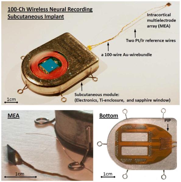
Photographs of the hermetically packaged 100-Ch fully implantable wireless neurosensing device.
Fig. 2.

SolidWorks (Waltham, MA, USA) model exploded view of the hermetically packaged 100-Ch fully implantable wireless neurosensing device.
Fig. 3.

(a) Circuit block diagram and (b) photographs of PCB-A and PCB-B for the hermetically packaged 100-Ch fully implantable wireless neurosensing device. The highlighted blocks in (a) are the custom designed ASICs and the rest are off-the-shelf components.
B. Preamplifier Printed Circuit Board (PCB-A)
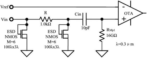
PCB-A integrates a custom application specific integrated circuit (ASIC) with 100 channels of preamplifiers and two analog multiplexers, two successive approximation ADCs, a controller ASIC, and a 48 MHz clock source. The incoming neural signal on each channel is conditioned and amplified by a low-noise low-power preamplifier implemented in the preamplifier ASIC. The design of a single low power preamplifier is shown in Fig. 4(a). The preamplifier uses a capacitive-feedback, folded cascode operational transconductance amplifier (OTA) configuration with a source follower output buffer. The closed-loop gain of the OTA is set by the ratio of the feedback voltage divider capacitors C2 and C3, which is 46 dB = 10 pF/0.05 pF. Large capacitor C4 = 6.8 pF is connected to the bodies of Mp4 and Mp5 to minimize the effect of their parasitic capacitors of on the gain of the preamplifier. The 5 pF capacitor CL across the OTA output provides the dominant pole for the opamp and sets the bandwidth of the circuit at 7.8 kHz. Any operational amplifier operating on a single power supply must have its output offset at the center of its output voltage range. The diode-connected MOSFETs, Mp4 and Mp5, effectively bypass C3 at very low frequency so a DC bias at the non-inverting input of the OTA can suitably offset the OTA output to 1.62 V, which is right at middle of its output range (1.0 V–2.3 V). The required bias is applied through the pMOS pseudo-resistor, RMp1. The 10 pF input capacitor C1 along with RMp1 forms an RC high-pass filter at 1/2πRMp1C1, where RMp1 is the equivalent resistance of the transistor Mp1. Many neural preamplifier designs [30]–[32] used diode-connected pMOS pseudo-resistor for this function. However, the problem with this diode connected scheme is that the high-pass frequency is very sensitive to process variation, especially to transistor threshold voltage variation. This is mainly due to the exponential relation between the gate-to-source voltage and the resistance of the device when it is biased in the subthreshold region. In the first version of the preamplifier ASIC [23], although RMp1 is independent of the threshold voltage, it is still exponentially dependent on the bias resistor R. Since the variation of R in the 0.5 μm 3M2P standard CMOS process could reach up to 30%, and the nominal bias voltage employed is 0.4 V, the worst case high-pass frequency variation can be as high as exp(0.4 × (1.3 – 1)/VT ≈ 100 times. To overcome this large variation, the bias resistor was intentionally removed from the ASIC and replaced with an external resistor. This external resistor can be appropriately chosen to compensate the high-pass variation from the fabrication process. In our implementation, the internal bias voltage Vref is set to 0.53 V. A 2.2 kΩ external resistor R sets RMp1 to be around 16 GΩ, which along with the 10 pF input capacitor set the high-pass frequency closed to 1 Hz. Vref also sets the OTA inputs bias to be 0.07 V and biases the input PMOS pair in subthreshold region to minimize thermal noise. Since the total input referred thermal noise of the preamplifier is given by
where k is Boltzmann constant, T is the absolute temperature in degree C. k usually has a value of 0.7 [31], gm3, gm5, and gm7 are the transconductances of corresponding transistors shown in Fig. 4(b). We had a better optimization on the noise-power trade-off for the preamplifier comparion to our previous work [9]. We used input PMOS pair with W/L of 960 μm/1.5 μm to achieve the maximum gm for a given bias current. Their sizes were large for 1/f noise reduction. We also reduced the gm of M5, M6, M7, and M8 by making their lengths large to minimize their thermal noise contribution. We measured the input referred noise of the preamplifier by grounding its input. As shown in Fig. 4(c), in our latest preamplifier ASIC, the noise optimization has brought down the in-band input referred noise and noise efficiency factor (NEF) to 2.83 μVrms and 3.3, respectively. Since the noise of the system is dominated by the thermal noise introduced by the microelectrodes, which is about 9–10 μVrms, the system still achieves an SNR > 6 dB for neural signals >100 μVpp. The measured common-mode rejection ratio (CMRR) and the power supply rejection ration (PSRR) are >60 dB and >50 dB, respectively. For details of the preamplifier design, please refer to [9].
Fig. 4.

(a) Schematic of the preamplifier design implemented within both versions of the 100-channel preamplifier ASIC. Note: the bias resistor R in the latest version has been pulled off-chip for post-fabrication high-pass adjustment. (b) Schematic of the OTA. (c) Noise spectrum density of the preamplifier shows an input referred noise of 2.83 μ Vrms over a frequency range of 1 Hz to 10 kHz, and an noise efficiency factor (NEF) of 3.3.
The circuit block diagram of the complete CMOS preamplifier ASIC is shown in Fig. 5 The entire 100 preamplifiers are divided into two groups of 50 preamplifiers each. A 48 MHz clock source was first divided by two to create the 24 MHz main clock for the system. The outputs from the preamplifiers in each group are multiplexed onto one of two analog outputs using the column and row select logic. This is run at a 1 MHz clock generated from the main 24 MHz clock and leads to a sampling rate of 20 kSps/Ch. The two multiplexed analog neural signals are buffered with unity gain buffers before they are fed into two commercial 12-bit SAR-ADCs (LTC2366 [33]). The two ADCs are running at 24 MHz clock rate with each ADC sample 24 clocks long, therefore provide 1 MSps for 50 channels (20 kSps/ch) and consume 4.8 mW at 3 V each. For every ADC sample, it contains a 10-clock sampling cycle with ADC output floating high and a 14-clock conversion cycle with 2 leading zeroes and 12 bits effective data. Both cycles are controlled by a chip select signal, which initiates the conversion cycle by active “LOW”. In order to combine the 12-bit effective data from each ADC into a single serial bit data stream, the multiplexing clocks for the two groups of preamplifiers as well as the ADCs' chip select signals are shifted by half an ADC sample from each other, the 10-clock sample cycle and the 2 leading zeroes of the conversion cycle from one ADC are masked by the 12 effective bits from the other ADC. Therefore the 24 Mbps digital stream contains back-to-back 12-bit sample data alternatively from both ADCs. A controller ASIC produces the aforementioned signals and manages the data flow between the preamplifier ASIC and the ADCs. ADC data is also packaged with a 24-bit synchronization pattern into a 24 Mbps digital data stream. This non-encoded data will make the data and clock recovery on the receiver side become difficult due to the fact that there is no clock component in its spectrum. Therefore a Manchester encoder was implemented with commercial off-the-shelf (COTS) components: two D flip-flops (SN74AUP2G80, Texas Instruments [34]) and a XOR gate (SN74LVC1G86, Texas Instruments [35]). The encoded 48 Mbps serial bit stream data is then fed into PCB-B for wireless transmission.
Fig. 5.

Circuit block diagram of the 100-Ch preamplifier ASIC.
The 100-channel preamplifier [Fig. 6(a)] and controller [Fig. 6(b)] ASICs were fabricated in the On Semiconductor 0.6 μm feature size 3M2P SCMOS_SUBM process and measure 5.2 × 4.9 mm2 and 2 × 2 mm2 respectively.
Fig. 6.
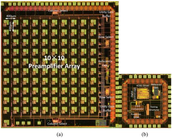
Microphotographs of the 100-ch preamplifier ASIC and the controller ASIC.
C. Power/Data Printed Circuit Board (PCB-B)
PCB-B (Fig. 3) shares the 3 V VDD and GND with PCB-A. It also takes the TTL format 48 Mbps Manchester encoded serial bit data stream: that modulates a freely running commercial VCO (SMV3460A-LF, Z-Communications Inc., [36]), which outputs 5 dBm 3.2 GHz to 3.8 GHz FSK power into a 1.5 dBi UWB chip antenna for wireless data broadcasting. This frequency is chosen for minimal interference between commercial wireless devices and our implantable device. An IR on-off switch is implemented as a new feature in the second version of the device using a silicon NPN phototransistor [37], which can detect IR light from 700 nm to 1100 nm with a peak spectral sensitivity at 880 nm. The phototransistor is powered directly from the battery. Upon receiving an IR pulse signal, the phototransistor induces a current pulse that passes through a 500 kΩ resistor to create a voltage pulse that drives a Schmitt trigger. The output of the Schmitt trigger toggles the enable pin of a global low-dropout linear regulator (LTC1844, Linear Technology [38]) that produces 3 V supply for the rest of the system from the battery voltage.
A wireless charger (BQ24108, Texas Instruments, [39]) is also implemented on PCB-B with COTS components to charge a medical grade 200 mAh Li-ion rechargeable battery (QL0200I-A, Quallion, [40]), which is able to operate the system for 6.6 hrs after it is fully charged. In order to reduce heat generation caused by the electromagnetic wave propagation loss in the implant (mostly in the Ti-enclosure) as well as in the primary coil, we reduced the power carrier frequency to 150 kHz from the original value of 2 MHz [23]. This is based on Maxwell's Electromagnetic Equations, where the power loss due to eddy currents in a conducting medium is given by P = (π Bdf)2/6kρD, where B is the magnetic field, d is the thickness of the material, f is the carrier frequency, k is a constant, and ρ and D are the resistivity and density of the material respectively [41]. Therefore the loss is proportional to f2. A 39 nF high-Q SMD 0603 ceramic capacitor along with a secondary coil forms an LC-tank for the wireless charger to harvest the 150 kHz RF energy from a 120 μH external primary coil driven by a Class-AB power amplifier. The secondary coil is a 27-turn 27 mm O.D. coil made from 46-AWG 40-strand Litz wire for minimum loss. It has a measured inductance value of 30 μH, serial resistance of 0.9 Ω, and a Q of 31.4 at 150 kHz. The received AC power is rectified by a full wave rectifier producing a 5 V DC supply for a switching mode Li-ion battery charger chosen for its >85% efficiency over a wide range of supply voltage (4.35 V–16 V) and charging current (0.1 A–2 A). The charging current is programmed to be 0.1 A (0.5C of the battery) taking 2 hrs to fully charge the battery after it is depleted. The wireless charger was designed with three safety features: a self-timer that terminates the charging within 2.5 hrs, a battery monitor that indicates the status of the battery, and a protection circuit module (PCM) that protects the battery from over-charging/discharging. Fig. 7 shows the measured charging efficiency of the implantable neurosensing device at different charging distances. The battery charging current reaches 92.4 mA@5 V at 3 mm distance with 800 mW input power going into the primary coil, which shows a 57.8% charging efficiency. The electronics on PCB-A and PCB-B along with the battery are encased in a 56 × 42 × 9 mm3 Ti-enclosure with a 29.2 mm diameter single crystal sapphire window. The secondary coil, chip antenna, IR on-off switch, and LED battery status indicators are placed directly below the sapphire window. There is less than 50% measured RF loss, and 86% IR on-off signal transmission considering the 14% reflection loss of sapphire with a refraction index of 1.756 at 980 nm [42] through the window.
Fig. 7.
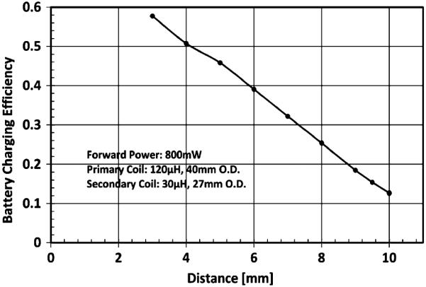
Measured charging efficiency of the implantable neurosensing device at different charging distances. The forward power is 800 mW at 150 kHz frequency. The charging efficiency is calculated by using the product of the charging current and the charging voltage (5 V) divided by the forward power.
III. ESD Safety and Patient Safety
The primary concern of any wireless implantable neurosensing devices is the safety of the subject. To evaluate the safety of our implantable neurosensing device, ESD test and patient safety test were conducted.
A. ESD Safety Test
The ESD human-body model (HBM) used for testing our device followed the internationally widely use JEDEC standard: JESD22-A114D [43]. The ESD protection circuit for each preamplifier is shown in Fig. 8. The circuit uses two relatively large NMOS transistors each consisting of six parallel devices having width to length ratios of 30 × 0.9 μm as the voltage limiting and energy absorbing elements. The gate and drain of each transistor are connected together to the signal line while the source and substrate connections are tied to ground. Ground connections to the substrate are made through large p+ diffusions adjacent to both source and drain and were designed to minimize the series resistance of the drain to substrate PN junction. Fig. 9(a) shows the I–V characteristics of these transistors as manufactured. The two transistors form a pi-network between the input pad and the input to the preamplifier. A 1 kΩ resistor, the third element of the pi-network, connects the two transistors. For a positive overvoltage input, the transistors act as diode-connected MOSFETs, turning on at the threshold voltage of 0.7 V. For a negative input, the drain to substrate junction is forward biased and the local substrate connections assure a low forward voltage even at high current. In both cases, the 1 kΩ resistor and the second NMOS device act as additional attenuation before the input surge voltage reaches the preamplifier input. This design guarantees that even if the surge voltage seen by the first stage NMOS exceeds the break down voltage of the input capacitor Cin and input PMOS gate oxide, the voltage applied to those elements will not. (For the 0.6 μm process, the gate oxide breakdown voltage is around ±15 V.) Comparing to other conventional complimentary silicon-controlled rectifier (SCR) structure and ggPMOS/ggNMOS pair structure [44], one advantage of this protection circuit is that it does not provide any path from the I/O pad to the supply voltage even after failure of either junctions or gate oxide. This is extremely important for patient safety, since it guarantees that there will be no direct circuit connection from a power source to the tissue through the input even when the input ESD protection is damaged.
Fig. 8.
ESD protection circuits for the preamplifier input on the 100-channel preamplifier ASIC using the two stage diode connected NMOS structure.
Fig. 9.
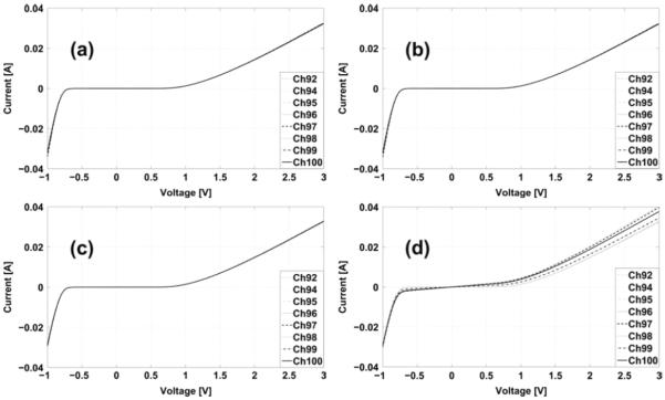
(a) The preamplifier input ESD protection circuit I-V before and (b) after Class 1A, (c) Class 1B, and (d) Class 1C ESD Testing. Results show that when the ESD protection circuit is intact, the forward and reverse biased conducting resistances are small with values around 7Ω and 50Ω at large bias voltages respectively.
The only electrical connections of the device that can be accessed externally are the 100 inputs of the preamplifier, hence the ESD safety test was carried out on those pins. Because the inputs of all preamplifiers are identical, we evaluated the ESD protection circuits in 8 channels out of 100 channels in the preamplifier ASIC. The ESD safety testing was done according to the Class 1A (250–500 V), Class 1B (500–1000 V), and Class 1C (1000–2000 V) JESD22-A114D ESD sensitivity classifications [43]. Fig. 9 shows the characteristics of the NMOS ESD protection circuits in 8 channels before and after the ESD test. These results show that the I–V curve of the NMOS devices remain unchanged after the 500 V Class 1A and 1000 V Class 1B ESD tests. After the 2000 V Class 1C ESD test, 4 out of 8 channels showed failures of their ESD protection circuits, degrading the input impedance on those channels to about 500 Ω to a few kΩ according to the slopes of the curves in Fig. 9(d) at low bias voltages. (The initial input impedance is higher than our instrument measurement range.) However, we believe that the input capacitor and the input PMOS gate oxide were unaffected by the 2000 V discharge pulse, since the amplifier gain and DC offset were the same after the test as before. The amplifier also remains insensitive to small (±50 mV) levels of DC input at the electrode pin.
B. Patient Safety Evaluation
The electrode-electrolyte interface between the MEA and the surrounding cerebrospinal fluid (CSF) will form a double layer capacitor with a dielectric layer one water molecule thick. Charging and discharging this double layer capacitor is an ideal mechanism of charge injection when there are no chemical changes in the tissue. However, the amount of charge that can be injected by the metal electrode to the double layer capacitor is only about 20 μC/cm2. Charge density in excess of this value will lead to the equivalent of the dielectric breakdown and onset of irreversible Faradaic reaction that is considered to be harmful to the patient [45]. To evaluate the patient safety of our device, the worst-case charge density was calculated when the voltage across the input capacitor is equal to the supply voltage of the system (3 V). In this case, the maximum charge that can deliver from the input to the tissue through the MEA electrode is 3 V × 10 pF = 3 × 10⁻⁵ μC. Since the minimum metal tip area of the MEA is in the order of 10−5 cm2, the maximum possible charge density deliver to the tissue through the device input is 3 μC/cm2. This value is about 7 times smaller than the safety limit and well within the safety levels. Even when the device ESD fails, as discussed earlier, the use of the two-stage diode connected NMOS ESD protection structure ensures that the input shorts to ground and there is no DC path from the supply source to the tissue. These tests give us further confidence that the device will be clinically safe for long-term patient use.
IV. Custom Wireless Receiver
An external superheterodyne receiver (shown in Fig. 10 with detailed part numbers) was developed to wirelessly receive the RF data. It uses a 10 dBi planar dual polarized antenna to reduce the motion sensitivity of the transmitter antenna. During the design phase, we measured the signal strength received by the 10 dBi antenna from the implanted device. It had a nominal value of −60 dBm at a few meters distance from the receiver. To accommodate and match the dynamic range of each block in the receiver according to this input signal level, the incoming 3.2 GHz to 3.8 GHz FSK signal is first amplified by two 24 dB LNAs with NF of 0.9 dB [46]. After that, it is down converted to 150 MHz to 750 MHz IF band by a wideband mixer [47] using an LO frequency at 3.05 GHz. The FSK-IF signal is then turned into an OOK-IF signal after the 750 MHz tone is filtered out by a 7th order 100 MHz Chebyshev band-pass filter centered at 150 MHz. After amplitude stabilization by an automatic-gain-control block [48], the OOK-IF is fed into an envelope detector that has two envelope filters with 70 MHz cutoff frequencies set by external capacitors [49]. Eventually, the baseband signal is restored, from which, the digital data and clock are extracted using a data/clock recovery block [50]. The recovered data is then forwarded to an FPGA and repackaged into 16-bit samples. Finally these samples of data get buffered though an 8 MB SDRAM and sent to a PC via USB 2.0 for further processing and visualization.
Fig. 10.

(a) Photograph and (b) block diagram of the RF superheterodyne receiver for the 100-ch wireless neural recording system.
The sensitivity performance of the RF receiver was evaluated using the test setup shown in Fig. 11. At first, a pseudorandom test pattern generator (TPG) using an external eighteen-bit linear feedback shift register (LFSR) was implemented in an FPGA. The external LFSR has a primitive polynomial P(x) = x18 + x7 + 1, which produces repeatable random sequences with the length of 218 − 1, which is long enough to be considered as a random signal. The pseudorandom pattern output from the FPGA was used to drive the same transmitter that was implemented in the device. The receiver picks up and recovers the FSK modulated pseudorandom digital signal as well as the clock with different received signal strengths. In the meantime, the original data was properly delayed, in such a way that it precisely aligned with the recovered data from the receiver. Finally, the error/difference between these two was calculated using an exclusive or function.
Fig. 11.
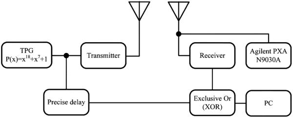
Bit error rate measurement setup for the custom RF receiver.
The input signal strength was measured at the receiver input using the Agilent PXA N9030A signal analyzer centered at 3.2 GHz and integrated over 100 MHz frequency range that equals to the receiver bandwidth. Since the PXA N9030A has a measured noise floor of −164.7 dBm/Hz even with the noise reduction option turned on, −84.7 dBm is the integrated noise power over 100 MHz bandwidth and indicates the minimum signal strength that can be measured using the setup shown in Fig. 11. The bit-error-rate (BER) of the receiver with different received signal strength is plotted in Fig. 12. It shows that at −77.7 dBm input single strength the receiver BER is around 10−8. The theoretical FSK BER curve of a non-coherent receiver is also shown in the figure as a comparison.
Fig. 12.

(a) Measured line-of-sight (LOS) received signal strength vs. distance using a 10 dBi planar antenna. (b) Measured BER for the receiver with different input signal strength using a 48 Mbps pseudorandom test pattern. The result is compared with the theoretical BER of a non-coherent FSK receiver.
The eye diagrams of the baseband data were also measured at different signal strengths using the Tektronix MSO5204 mixed signal oscilloscope and its advanced jitter, timing, and eye diagram analysis software DPOJET. As shown in Fig. 13, the received baseband signal eye diagrams with input signal strengths of (a) −41.1 dBm, (b) −47.6 dBm, (c) −57.8 dBm, and (d) −78.1 dBm at 33 Mbps were measured. The eye heights and widths are, respectively, 622 mV/28.7 ns for −41.1 dBm input, and 152.4 mV/14 ns for −78.1 dBm.
Fig. 13.

Measured eye diagram of the received baseband signal with different input signal strengths using a 33 Mbps pseudorandom test pattern. (a)–41.1 dBm input power. (b) –47.6 dBm input power. (c) –57.8 Bm input power. (d) –78.1 dBm input power. (e) Based band data pulse width and amplitude deviation summary.
V. Bench Top Measurements of the Full Wireless System
The full functionality and performance of the entire system (the neurosensing implant and the receiver) were tested on bench. As shown in Fig. 14, 1 mVpp artificial neural spike signals at 100 Hz were applied to all inputs of the 100-channel neurosensing device. The broadcasted RF data was received at a 1 m distance away and the recovered artificial spikes were stored and visualized in real-time by a home-made graphic user interface (GUI) collecting data over a high speed USB link. Meantime, a Gigabit Ethernet user interface is also developed to provide higher volume data rate and versatile data storage and visualization capabilities.
Fig. 14.
1 mVpp 100 Hz artificial spike signals recorded wirelessly using the 100-channel implantable neurosensing device at a 1 m distance.
The IR on-off switch was shown to function well in both bench top and in vivo testing. The irradiance of the IR on-off signal from a 980 nm 50 mW IR laser pointer directly pointed at the sapphire window through a 2 cm pig skin was measured to be ~1μW/cm2 at the top surface of the device after the reflection, scattering, and absorption loss through the skin. It was found that there is a 14% further reduction of the signal due to the sapphire window. The final irradiance induced a current around 6 μA in the phototransistor that is high enough to turn on the device after the implantation. As discussed in our early publication [23], the temperature increase due to charging (eddy currents in Ti-enclosure) is obviously a major concern for the first version of the device that uses 2 MHz power carrier. The FDA mandates that a device has to meet the ISO 14708–1:2000 E standard requiring no outer surface of a device rise more than 2°C above body temperature (37°C). We have lowered the power carrier down to ~150 kHz in the second version and observed a dramatic reduction of heat induced temperature rise to only a few degree C in room air, which is expected to be much lower in a real animal due to the larger thermal conductivity and perfusion rate of the blood vessels and tissue [51].
A summary of the measured specifications of the second version of the device is shown in Table I. In addition, a system comparison of the presented device with other state-of-the-art designs is listed in Table II.
TABLE I.
Measured Performance of the Second Version 100-Channel Wireless Neurosensing Device
| The Measured Performance of the 2nd Version 100-Ch Fully Implantable Wireless Neurosensing Device | |
|---|---|
| Number of channel | 100 |
| Preamplifier gain, bandwidth, and input referred noise | 200 (46dB), 1 Hz(tunnable) ~ 7.8 kHz, 2.83μVrms |
| Preamplifier ASIC size and power dissipation | 5.2×4.9mm2. 6mW@3V |
| Controller ASIC size and power dissipation | 2×2mm2, 10mW@3V (9mW for VCSEL driver) |
| System resolution and sampling rate | 12 bils for all channels, 2 MSps (20 kSps/Ch) |
| Data encoding | Manchester (48Mbps) |
| RF FSK Tx frequency and power dissipation | 3.2/3.8 GHz, 50mW |
| IR on-off switch wavelength | 980nm |
| Inductive power carrier and charging efficiency | 150kHz, 57.8%@3mm |
| RF receiver sensitivity | −77.7dBm@48Mbps with 10−8 BER |
| Battery | 200mAh medical grade I.i-ion rechargeable battery |
| Battery operational hours after fully charged | 6.6hrs |
| Total power dissipation (when not charging) | 30.2mA@3V |
| Titanium enclosure dimension with overmold | 56×42×11mm3 |
| Total weight of the system | 44.5g (7.4g for battery, 30.6g for the Ti-enciosure) |
TABLE II.
Comparison of State-of-the-Art Wireless Neural Recording Systems
| Ref | Type | Mode Tested | Amp BW Hz | Noise μVrms | Res Bits | S/ch ksps | # Ch | Data rate Mbps | Power mW | Size mm | Tx |
|---|---|---|---|---|---|---|---|---|---|---|---|
| (Chae, et al., 2009) [19] | Chip | Bench | 0.1, 200–2.2k configurable | 4.9 | 6–9 | 2 | 128 | 90 | 6 | 8.8×7.2 | UWB |
| (Harrison, et al., 2009) [13] | Chip | Bench | 250–5k | 5.0 | 10 | 15 | 100 | 0.345 | 10 | 5.4×4.7 | 902/928 FSK |
| (Shahrokhi, et al., 2010) [20] | Chip | Bench | 10–5k | 6.08 | 8 | 14 | 128 | n.a. | 9.33(Rec. +Stim.) | 3.4×2.5 | n.a. |
| (Gao, et al., 2012) [11] | External | Bench | <1–10k, 280–10k | 2.2 | 10 | 31.25 | 96 | 30 | 30(IC+Tx+FPGA) | 5×5(IC) | UWB |
| (Greenwald, et al., 2010) [18] | External | Rodent | n.a.-8.2k | 1.94 | 10 | 16 | 16 | 0.256(IC) 1 (UWB) | 15.84 | 24000mm3 | UWB |
| (Miranda, et al., 2010) [10] | External | Primate 3 month | <1–4.5k | 5.0 | 12 | 30 | 32 | 24 | 142 | 38×38×51 | 3.7/4.1GHz FSK |
| (Yin, et al., 2010) [17] | External | Rodent | 1–8.8k configurable | 4.9 | 8 | 20 | 32 | 2.56 | 5.6 | n.a. | 898/926MHz FSK |
| (Szuts, et al., 2011) [21] | External | Rodent 1hr | 10–4.5k configurable | 3.64 | Analog | 20 | 64 | 10 | 645 | n.a. | 2.38GHz FM |
| (Sodagar, et al., 2009) [22] | External | Guinea Pig | <100–10k configurable | 8.87 | 8 | 7.8 | 64 | 2 | 14.4 | 14.4×15.5 | 70 – 200MHz OOK |
| (Rizk, et al., 2007) [13] | External | Rodent | 500–8k | n. a. | 12 | 31.25 | 96 | 1 | 100 | 50×40×15 | 916.5 MHz ASK |
| (Rizk, et al., 2009)[14] | Implanted | Sheep 3hrs | n.a. | 7 | 12 | 31.25 | 96 | n.a. | 2000 | 50×40×15 | 916.5 MHz ASK |
| (Rouse, et al., 2011)[12] | Implanted | Primates | DC-500 configurable | 1(5Hz band) | n.a. | n.a | 4 | 0.0117 | 0.04 | n.a. | 175kHz |
| This work | Implanted | Swine & Primate >14 months | 0.1–7.8k configurable | 8.05/2.83 | 12 | 20 | 100 | 48 Manchester encoded | 90.6 | 52×46×11 | 3.2/3.8 GHz FSK |
VI. In Vivo Testing
Following the bench top measurements, the full functionality of the entire wireless neural recording system was validated in vivo in two adult awake Yorkshire swine [52] and two rhesus macaque monkeys over a period of more than a year. Fig. 15(a) shows a cartoon of the device implantation and array placement. In order to properly implant the device into those animals, specific surgical procedures were developed. The procedure usually started with a skin incision to expose the cranium after the preparation of the animal. A craniotomy was then made gain access to the intracranial space. The dura mater was then incised and reflected to expose the cortex. The Ethylene-Oxide sterilized device was then place in the surgical area and the titanium enclosure part was secured on to the skull using titanium bone screws. The microelectrode array (MEA) was carefully guided by the wirebundle and place a few millimeters above the target cortical location. In this case, we used the well-defined primary somatosensory cortex (SI) and the primary motor cortex (MI) for the swine model and the rhesus macaque monkey model respectively for their value towards neuroprosthetic research interests. The final insertion of the 1.5 mm MEA needle was then made by a pneumatic drive (Blackrock Microsystems) at 172 kPa. Following the insertion, the dura was sutured back and the bone-flap from the craniotomy was restore and secured onto the cranium to protect the cortex and MEA. Finally, the skin was sutured back in the swine model cases. For the rhesus macaque monkey model cases, since their skulls were significantly smaller than human skull and insetting the device was not possible, the closure of the skin would have been difficult. We decided not to close the skin to prevent subsequent problems that might compromise the superficial vasculature and skin integrity in these first two non-human primate implant experiments. However, recently, we were able to successfully fully implant our device into a monkey with slightly larger skull size. The detailed results will be reported elsewhere.
Fig. 15.

(a) A cartoon of the device implantation and array placement. (b) X-ray images of the implantable device in a swine and a rhesus macaque.
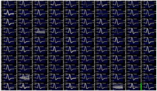
During recording sessions, the systems were successfully recharged and powered up with channels showed consistent input referred noise level of ~9 μVrms. This noise is mostly due to the physiological background noise and the electrode thermal noise. The neural spikes extracted from 10 seconds sample of recorded data from a Yorkshire pig (SU) are shown in Fig. 16(a) using a 6th order Butterworth filter with bandwidth from 300–5000 Hz. 48 channels out of 100 show clear neural spikes with an amplitude range from 60 to 160 μVpp . LFPs were also extracted from the data (the bottom traces of the Fig. 16) using filter with bandwidth from 0.1–300 Hz as this spectrum range is being increasingly used in neuroscientific research. Fig. 16(b) shows the counterpart data measured in a rhesus macaque monkey (JV) with 93 out 100 channels showing neural spikes with an amplitude range from 60 to 350μVpp. The insets at the top left corner of each 10 × 10 grid in Fig. 16 show examples of the channels that have multiple units. The insets to the left of each LFP trace show the zoom-in view of the spikes.
Fig. 16.

(a) Simultaneously recorded in vivo neural spikes from an awake Yorkshire swine and (b) a rhesus macaque monkey using the 100-Channel fully implanted wireless neurosensing device. The 100-channel sorted neural spikes are displayed in a 10 × 10 grid showing in the top column of the figure. The insets at the top left corner of each grid show examples of the channel that has multiple units. The bottom column of the figure shows the spike signal and LFP signal extracted from a signal channel. The insets on the left of each LFP trace show the zoom-in view of the spikes.
In addition, we have used the spike data to interpret and differentiate the particular movements associated with the animals' natural behavior by projecting the multidimensional spike train data onto a two-dimensional representation of neural trajectories [Fig. 17(a)]. Here, spiking data from each channel was run through a spike extraction operator of choice (we use the multiresolution Teager energy operator, MTEO [53]) to calculate a running firing rate. The extracted neural action potentials were then binned every 100 ms and smoothed with a Gaussian kernel yielding the smoothed firing rate on each channel. Principal component analysis (PCA) was used to align the smoothed firing rate of each input channel by contribution to the variance in the signal. When observed dynamically over time, the first two principal components are often termed “neural trajectory”. These were used to describe the dynamic state changes of the cortical network. This method of analysis is well documented elsewhere [54]–[56] and provides a low-dimensional representation of the dynamical state of the brain. We present neural trajectories produced during free movement of monkey JV: scratching eye (blue), touching an apple (green) and turning head (purple) in Fig. 17. Circles represent the centroids of trajectory during each movement. The ability to record natural movements from a distance without disturbing the subject brings with it the potential for new insights into the subtleties of motor dynamics and into the cortical pathways controlling movement. Additional details of the animal experiments with this wireless implant are given elsewhere [57].
Fig. 17.

Wirelessly recorded data from the neurosensing device implanted in a rhesus macaque monkey. (a) and (b) Threshold crossings across all channels can be reduced to a low-dimensional state space through principal component analysis (among other methods). We present such neural trajectories produced during free movement of monkey JV: scratching eye (blue), touching an apple (green) and turning head (purple). Circles represent centroids of trajectory during each movement. (c) A selection of 15/100 broadband recording channels demonstrating heterogeneity of the neural signals and the richness of high-sample rate data collection (20 kSps). (d) A raster plot (12 s) marking threshold-crossing timestamps for all input channels and behavior is indicated by color: scratching eye (blue), touching an apple (green) and turning head (purple).
VII. Conclusion and Discussion
We have presented the implementation of a 100 channel fully head implantable wireless broadband neural recording system with inductively rechargeable battery and RF data transfer. The prototype device system is viewed by us as a platform for translation to human neuroprothesis and potential brain disease diagnosis applications, while of potential importance also for behavioral neuroscience research in freely moving animals. The details of the system architecture and circuitry were presented with specific innovations and features not previously available in an active neural implant. The full functionality of the device has been demonstrated through bench-top measurements as well as in vivo wireless recording in two freely moving Yorkshire pigs and two freely moving rhesus macaque monkeys. Robust neural spikes and LFP signals from cortical microcircuits were acquired wirelessly. In addition to beginning the path to human translation, we are actively working on implementing this device in non-human primate models for freely moving behavioral research applications such as motor planning for arm and hand movements. Initial trials in such primate have been productive and preliminary behaviorally related neural data with decoded neural trajectories from a freely moving monkey are illustrated in this paper.
In addition to results in freely moving animal model, we note that there is further opportunity for improvement. First, although the eddy current and skin effect induced heat in the Ti-enclosure was much reduced by lowering the power carrier, we are also performing FEM modeling and in vivo measurements to characterize heat generation on the current version of the device for further optimization. Meanwhile, using different grades of titanium alloy with larger electrical resistivity for the enclosure might lower the eddy current loss in the Ti-enclosure (loss is reverse proportional to the electrical resistivity of the material). For example, Our present devices use Grade 2 titanium alloy with an electrical resistivity of 5.2 × 10⁻⁵ Ωω·cm [58], while e.g., Grade 5 titanium alloy has a value of 1.8 × 10⁻⁴ Ωω·cm [59], though must be able to accommodate the fabrication requirements of the hermetically sealed, high density feedthrough configuration. Second, nearly half the power consumption of the present device is used by the COTS RF transmitter. We are presently developing a custom RF transmitter ASIC, targeted to consume approximately 1/3 power dissipation of the COTS transmitter while still transmitting comparable RF power of approximately 5 dBm. In addition, the simple Manchester encoding scheme used for the data doubles the data rate and is not as bandwidth efficient as other methods. We are working on investigating advanced encoding methods, such as 8 b/10 b line code [60], [61] (widely used in serial ATA, Gigabit Ethernet, and USB3.0), to improve bandwidth efficiency, achieve DC-balance and bounded disparity, while still maintain sufficient state changes for clock recovery. The last and most important improvement needed is in regard to the natural behavior of the freely moving animal. Currently, our wireless data link can experience fading issues caused by either multipath or shadowing effects. In order to improve the reliability of the link, we are currently also investigating the multiple-input and multiple-output (MIMO) concept [62]–[64] (which is implemented in modern wireless communication standards such as IEEE 802.11n, 4G, LTE, and WiMAX) for our next generations of implantable, wireless, broadband neurosensing devices.
Acknowledgment
The authors acknowledge the roles of Cirtec Medical Inc., Microconnex Inc., CVInc., and Blackrock Microsystems Inc., in their important role for fabricating specific components of the implantable device. They thank the following doctors, J. Barrese, M. Goddard, S. Cash, L. Hochberg, and J. Donoghue, for their surgical and neurological expertise. They acknowledge Kineteks Inc. for fabricating the sterilizable and static-dissipative holder for devices through a constructive collaboration. Many members of the Brown University Neuroengineering Laboratory made key contributions. In particular, they thank C. Bull and N. Agha. The expertise and dedication of the staff of the Brown University Animal Care Facility was invaluable, and they thank Dr. J. Harper, V. Budz, R. Burrill, and P. Norberg. All animal experiments were conducted according to Institutional Animal Care and Use Committee guidelines and the USDA under protocol #0911091.
This work was supported in part by the National Institute of Health (NIBIB and NCMRR/NICHD, 1R01EB007401-01), the National Science Foundation under the EFRI Program (0937848), and the DARPA Repair Program. This paper was recommended by Associate Editor S. Carrara.
Biographies
Ming Yin (S'06–M'10) received the B.S. and M.S. degrees in electronics engineering from Tsinghua University, Beijing, China, and the Ph.D. degree in electrical engineering from North Carolina State University, Raleigh, NC, USA, in 2001, 2004, and 2009, respectively.
From 2009 to 2013, he worked as a Postdoctoral Fellow at Brown University, Providence, RI, USA. Currently, he is an Assistant Professor, Research, in the School of Engineering at Brown University. His research interests include low noise, low power analog/mixed circuit design for wireless biomedical devices.

David A. Borton (S'06–M'12) was born in Seattle, WA, USA. He received the B.S. degree in biomedical engineering from Washington University in St. Louis, St. Louis, MO, USA, and the Ph.D. in biomedical engineering from Brown University, Providence, RI, USA, in 2006 and 2012, respectively.
His thesis work on implantable neuroprostheses was supported by the Brown Institute for Brain Science through a Reismen and Dana Mahoney Fellowship. Currently, he is a Research Associate and Marie Curie International Fellow at the Swiss National Institute of Technology (EPFL), Lausanne, Switzerland, where he develops neurotechnology to study neuromotor disease and injury.

Juan Aceros (M'01) received the M.S. degree in mechanical engineering and the Ph.D. degree in electrical engineering from Northeastern University, Boston, MA, USA.
From 2009 to 2013, he was a Senior Research Associate with the Neuroengineering Laboratory at Brown University, Providence, RI, USA. Since 2013, he has been an Assistant Professor of Engineering at the University of North Florida, Jacksonville, FL, USA. His research interests are in the area of fabrication of implantable neuroengineering devices, assistive technologies, and topics related to micro/nano fabrication and MEMS.
Dr. Aceros is a member of the Materials Research Society (MRS), the America Society of Mechanical Engineers (ASME).

William R. Patterson (M'73) received the B.Sc. degree in physics and the M.Sc degree in electrical engineering from Brown University, Providence, RI, USA, in 1963 and 1966, respectively.
Since 1977, he has been with the Electrical Sciences Group, Division of Engineering, Brown University, where he is currently a Senior Lecturer and Senior Research Engineer. His research interests include low-power analog circuit design for biomedical applications, circuits, and architectures for microphone array technology.

Arto V. Nurmikko (M'90–SM'97–F'99) was born in Finland. He received the B.S., M.S., and Ph.D. degrees in electrical engineering from the University of California, Berkeley, Berkeley, CA, USA.
Currently, he is the L. Herbert Ballou University Professor of Engineering and Physics at Brown University, Providence, RI, USA. His research involves basic physical and neuroscience, including application of device technology concepts to neuroengineering.
Dr. Nurmikko is a Fellow of the American Physical Society and the Optical Society of America, and member of the American Academy of Arts and Sciences.
References
- [1].Simeral JD, Kim SP, Black MJ, Donoghue JP, Hochberg LR. Neural control of cursor trajectory and click by a human with tetraplegia 1000 days after implant of an intracortical microelectrode array. J. Neural Eng. 2011 Apr;8(2):025027. doi: 10.1088/1741-2560/8/2/025027. [DOI] [PMC free article] [PubMed] [Google Scholar]
- [2].Hochberg LR, Bacher D, Jarosiewicz B, Masse NY, Simeral JD, Vogel J, Haddadin S, Liu J, Cash SS, van der Smagt P, Donoghue JP. Reach and grasp by people with tetraplegia using a neurally controlled robotic arm. Nature. 2012 May;485(7398):372–375. doi: 10.1038/nature11076. [DOI] [PMC free article] [PubMed] [Google Scholar]
- [3].Velliste M, Perel S, Spalding MC, Whitford AS, Schwartz AB. Cortical control of a prosthetic arm for self-feeding. Nature. 2008 Jun;453(7198):1098–1101. doi: 10.1038/nature06996. [DOI] [PubMed] [Google Scholar]
- [4].Truccolo W, Donoghue JA, Hochberg LR, Eskandar EN, Madsen JR, Anderson WS, Brown EN, Halgren E, Cash SS. Single-neuron dynamics in human focal epilepsy. Nature Neurosci. 2011 May;14(5):635–641. doi: 10.1038/nn.2782. [DOI] [PMC free article] [PubMed] [Google Scholar]
- [5].Afshar A, Santhanam G, Yu BM, Ryu SI, M. S., Shenoy KV. Single-trial neural correlates of arm movement preparation. Neuron. 2011 Aug;71(3):555–564. doi: 10.1016/j.neuron.2011.05.047. [DOI] [PMC free article] [PubMed] [Google Scholar]
- [6].O'Doherty JE, Lebedev MA, Ifft PJ, Zhuang KZ, Shokur So., Bleuler H, Nicolelis MAL. Active tactile exploration using a brain-machine-brain interface. Nature. 2011 Nov;479(7372):228–231. doi: 10.1038/nature10489. [DOI] [PMC free article] [PubMed] [Google Scholar]
- [7].Nurmikko AV, Donoghue JP, Hochberg L, Patterson WR, Song Y-K, Bull C, Borton D, Laiwalla F, Park S, Yin M, Aceros J. Listening to brain microcircuits for interfacing with external world-progress in wireless implantable microelectronic neuroengineering devices. Proc. IEEE. 2010 Mar;98(3):375–388. doi: 10.1109/JPROC.2009.2038949. [DOI] [PMC free article] [PubMed] [Google Scholar]
- [8].Patterson WR, Song Y-K, Bull CW, Deangelis AP, Lay C, McKay JL, Nurmikko AV, Donoghue JP, Connors BW. A microelectrode/microelectronic hybrid device for brain implantable neuroprosthesic applications. IEEE Trans. Biomed. Eng. 2004 Oct;51(10):1845–1853. doi: 10.1109/TBME.2004.831521. [DOI] [PubMed] [Google Scholar]
- [9].Aceros J, Yin M, Borton DA, Patterson WR, Nurmikko AV. A 32-channel fully implantable wireless neurosensor for simultaneous recording from two cortical regions. Proc. IEEE 33th Engineering in Medicine and Biology Soc. Conf.; Aug. 2011. pp. 2300–2306. [DOI] [PMC free article] [PubMed] [Google Scholar]
- [10].Miranda H, Gilja V, Chestek CA, Shenoy KV, Meng TH. HermesD: A high-rate long-range wireless transmission system for simultaneous multichannel neural recording applications. IEEE Trans. Biomed. Circuits Syst. 2010 Jun;4(3):181–191. doi: 10.1109/TBCAS.2010.2044573. [DOI] [PubMed] [Google Scholar]
- [11].Gao H, Walker RM, Nuyujukian P, Makinwa KAA, Shenoy KV, Murmann B, Meng TH. HermesE: A 96-channel full data rate direct neural interface in 0.13 um CMOS. IEEE J. Solid State Circuits. 2012 Apr;47(4):1043–1054. [Google Scholar]
- [12].Rouse AG, Stanslaski SR, Cong P, Jensen RM, Afshar P, Ullestad D, Gupta R, Molnar GF, Moran1 DW, Denison TJ. A chronic generalized bi-directional brain-machine interface. J. Neural Eng. 2011 May;8:036018. doi: 10.1088/1741-2560/8/3/036018. [DOI] [PMC free article] [PubMed] [Google Scholar]
- [13].Harrison RR, Kier RJ, Chestek CA, Gilja V, Nuyujukian P, Ryu S, Greger B, Solzbacher F, Shenoy KV. Wireless neural recording with single low-power integrated circuit. IEEE Trans. Neural Syst. Rehabil. Eng. 2009 Aug;17(4):322–329. doi: 10.1109/TNSRE.2009.2023298. [DOI] [PMC free article] [PubMed] [Google Scholar]
- [14].Avestruz A, Santa W, Carlson D, Jensen R, Stanslaski S, Helfenstine A, Denison T. A 5 μW/channel spectral analysis IC for chronic bidirectional brain-machine interfaces. IEEE J. Solid-State Circuits. 2008 Dec;43(12):3006–3024. [Google Scholar]
- [15].Rizk M, Obeid I, Callender SH, Wolf PD. A single-chip signal processing and telemetry engine for an implantable 96-channel neural data acquisition system. J. Neural Eng. 2007 Sep;4(3):309–21. doi: 10.1088/1741-2560/4/3/016. [DOI] [PubMed] [Google Scholar]
- [16].Rizk M, Bossetti CA, Jochum TA, Callender SH, Nicolelis MAL, Turner DA, Wolf PD. A fully implantable 96-channel neural data acquisition system. J. Neural Eng. 2009 Apr;6(2):026002. doi: 10.1088/1741-2560/6/2/026002. art. [DOI] [PMC free article] [PubMed] [Google Scholar]
- [17].Yin M, Ghovanloo M. A low-noise clockless simultaneous 32-channel wireless neural recording system with adjustable resolution. Analog Integr. Circuits Signal Proc. 2011 Mar;66(3):417–431. [Google Scholar]
- [18].Greenwald E, Mollazadeh M, Thakor N, Tang W, Culurciello E. A VLSI neural monitoring system with ultra-wideband telemetry for awake behaving subjects. Proc. IEEE Int. Symp. Circuits and Systems; Paris, France. 2010. pp. 1193–1196. [DOI] [PubMed] [Google Scholar]
- [19].Chae M, Liu W, Yang Z, Chen T, Kim J, Sivaprakasam M, Yuce M. A 128-channel 6 mW wireless neural recording IC with on-the-fly spike sorting and UWB transmitter. Proc. IEEE Int. Solid-State Circuits Conf.; Feb. 3-7, 2008. pp. 146–603. [Google Scholar]
- [20].Shahrokhi F, Abdelhalim K, Serletis D, Carlen P, Genov R. 128-Channel fully differential digital integrated neural recording and stimulation interface. IEEE Trans. Biomed. Circuits Syst. 2010 Jun;4(3):149–161. doi: 10.1109/TBCAS.2010.2041350. [DOI] [PubMed] [Google Scholar]
- [21].Szuts T, Fadeyev V, Kachiguine S, Sher A, Grivich MV, Agrochão M, Hottowy P, Dabrowski W, Lubenov EV, Siapas AG, Uchida N, Litke AM, Meister M. A wireless multi-channel neural amplifier for freely moving animals. Nature Neurosci. 2011;14(263) doi: 10.1038/nn.2730. [DOI] [PubMed] [Google Scholar]
- [22].Sodagar AM, Perlin GE, Yao Y, Najafi K, Wise KD. An implantable 64-channel wireless microsystem for single-unit neural recording. IEEE J. Solid-State Circuits. 2009;44(9):2591–2604. [Google Scholar]
- [23].Yin M, Borton DA, Aceros J, Patterson WR, Nurmikko AV. A 100-channel hermetically sealed implantable device for wireless neurosensing applications. Proc. IEEE Int. Symp. Circuits and Systems. 2012 May;:2629–2632. doi: 10.1109/TBCAS.2013.2255874. [DOI] [PMC free article] [PubMed] [Google Scholar]
- [24].Jones KE, Campbell PK, Normann RA. A glass/silicon composite intracortical electrode array. Ann. Biomed. Eng. 1992 Jul;20(4):423–437. doi: 10.1007/BF02368134. [DOI] [PubMed] [Google Scholar]
- [25].Nordhausen C, Maynard E, Normann RA. Single unit recording capabilities of a 100 microelectrode array. Brain Res. 1996;726(1–2):129–140. [PubMed] [Google Scholar]
- [26].Rousche PJ, Normann RA. Chronic recording capability of the Utah intracortical electrode array in cat sensory cortex. J. Neurosci. Methods. 1998;82(1):1–15. doi: 10.1016/s0165-0270(98)00031-4. [DOI] [PubMed] [Google Scholar]
- [27].Blackrock Microsystems, Utah Array [Online] Available: http://www.blackrockmicro.com/userfiles/file/Microelectrode%20Arrays.pdf.
- [28].Seligman P. Prototype to product-developing a commercially viable neural prosthesis. J. Neural Eng. 2009 Oct;6(065006) doi: 10.1088/1741-2560/6/6/065006. [DOI] [PubMed] [Google Scholar]
- [29].NuSil Technology MED-4211 [Online] Available: http://www.nusil.com/library/products/MED-4211P.pdf.
- [30].Olsson RH, III, Gulari MN, Wise KD. A fully integrated bandpass amplifier for extracellular neural recording. Proc. 1st Int. IEEE Engineering in Medicine and Biology Soc. Conf. Neural Engineering; Mar. 2003. pp. 165–168. [Google Scholar]
- [31].Harrison RR, Charles C. A low-power, low-noise CMOS amplifier for neural recording applications. IEEE J. Solid-State Circuits. 2003 Jun;38(6):958–965. [Google Scholar]
- [32].Wattanapanitch W, Fee M, Sarpeshkar R. An energy-efficient micropower neural recording amplifier. IEEE Trans. Biomed. Circuits Syst. 2007 Jun;1(2):136–147. doi: 10.1109/TBCAS.2007.907868. [DOI] [PubMed] [Google Scholar]
- [33].Linear Technology Corporation LTC2366—3 Msps, 12-Bit Serial ADCs in TSOT-23 [Online] Available: http://www.linear.com/product/LTC2366.
- [34].Texas Instruments SN74AUP2G80 [Online] Available: www.ti.com/lit/ds/symlink/sn74aup2g80.pdf.
- [35].Texas Instruments SN74LVC1G86 [Online] Available: www.ti.com/lit/ds/symlink/sn74lvc1g86.pdf.
- [36].Z-Communications Inc. SMV3460A-LF [Online] Available: http://www.zcomm.com/PDFs/datasheets/SMV3460A-LF.pdf.
- [37].Vishay Intertechnology Inc. TEMT1000 Silicon NPN Phototransistor [Online] Available: http://www.vishay.com/docs/81554/temt1000.pdf.
- [38].Linear Technology LTC1844 [Online] Available: http://www.linear. com/product/LTC1844.
- [39].Texas Instruments BQ24108 [Online] Available: http://www.ti.com/product/bq24108.
- [40].Quallion, QL0200I-A [Online] Available: http://www.quallion.com/new-pdf/QL0200IA.pdf.
- [41].Fiorillo F. Measurement and Characterisation of Magnetic Materials. Elsevier Academic Press; Amsterdam, The Netherlands: 2004. p. 31. ISBN 0-12-257251-3. [Google Scholar]
- [42].Refraction Index of Sapphire [Online] Available: http://www.quartz-silica.net/sapphire.htm.
- [43].ESD HBM JEDEC Standard [Online] Available: http://www.syncpower.com/datasheet/JEDEC%20HBM.pdf.
- [44].Wang AZ, Feng HG, Gong K, Zhan RY, Stine J. On-chip ESD protection design for integrated circuits: An overview for IC designers. Microelectron. J. Elsevier Sci. 2001 Sep;32(9):733–747. [Google Scholar]
- [45].Agnew WF, McCreery DB. Neural Prostheses: Fundamental Studies. Vol. 27. Prentice Hall; Englewood Cliffs, NJ, USA: 1990. ISBN 0-13-615444-1. [Google Scholar]
- [46].Mini-Circuits, ZX60-3800LN+ Low Noise Amplifier [Online] Available: http://www.minicircuits.com/pdfs/ZX60-3800LN+.pdf.
- [47].Analog Devices, ADL5801, High IP3 10 MHz to 6 GHz Active Mixer [Online] Available: http://www.analog.com/static/imported-files/data_sheets/ADL5801.pdf.
- [48].Analog Devices, AD8367, 500 MHz Linear-in-dB VGA With AGC Decector [Online] Available: http://www.analog.com/static/imported-files/data_sheets/AD8367.pdf.
- [49].Analog Devices, ADL5511, DC-6 GHz Envelope&TruPwr RMS Detector [Online] Available: http://www.analog.com/static/imported-files/data_sheets/ADL5511.pdf.
- [50].Analog Devices, Inc. ADN2814 Continuous Rate 10 Mb/s to 675 Mb/s Clock and Data Recovery IC With Integrated Limiting Amp [Online] Available: http://www.analog.com/static/imported-files/data_sheets/ADN2814.pdf.
- [51].Van Leeuwen GMJ, Lagendijk JJW, Van Leersum BJAM, Zwamborm APM, Hornsleth SN, Kotte ANTJ. Calculation of change in brain temperatures due to exposure to a mobile phone. Phys. Med. Biol. 1999;44:2367–2379. doi: 10.1088/0031-9155/44/10/301. [DOI] [PubMed] [Google Scholar]
- [52].Borton D, Yin M, Aceros J, Agha N, Minxha J, Komar J, Patterson WR, Bull C, Nurmikko AV. Developing implantable neuroprosthetics: A new model in pig. Proc. IEEE 33th IEEE Engineering in Medicine and Biology Soc. Conf.; Aug. 2011. pp. 3024–3030. [DOI] [PMC free article] [PubMed] [Google Scholar]
- [53].Choi JH, Jung HK, Kim T. A new action potential detector using the MTEO and its effects on spike sorting systems at low signal-to-noise ratios. IEEE Trans. Biomed. Eng. 2006 Apr;53(4):738–746. doi: 10.1109/TBME.2006.870239. [DOI] [PubMed] [Google Scholar]
- [54].Afshar A, Santhanam G, Yu BM, Ryu SI, Sahani M, Shenoy KV. Single-trial neural correlates of arm movement preparation. Neuron. 2011 Aug;71(3):555–564. doi: 10.1016/j.neuron.2011.05.047. [DOI] [PMC free article] [PubMed] [Google Scholar]
- [55].Santhanam G, Yu BM, Gilja V, Ryu SI, Afshar A, Sahani M, Shenoy KV. Factor-analysis methods for higher-performance neural prostheses. J. Neurophys. 2009 Aug;102(2):1315–1330. doi: 10.1152/jn.00097.2009. [DOI] [PMC free article] [PubMed] [Google Scholar]
- [56].Yu BM, Cunningham JP, Santhanam G, Ryu SI, Shenoy KV, Sahani M. Gaussian-process factor analysis for low-dimensional single-trial analysis of neural population activity. J. Neurophys. 2009 Jul;102(1):614–635. doi: 10.1152/jn.90941.2008. [DOI] [PMC free article] [PubMed] [Google Scholar]
- [57].Borton DA, Yin M, Aceros J, Nurmikko AV. An implantable wireless neural interface for recording cortical circuit dynamics in moving primates. J. Neural Eng. 2013 Feb 21;10(2):026010. doi: 10.1088/1741-2560/10/2/026010. [DOI] [PMC free article] [PubMed] [Google Scholar]
- [58].Titanium Grade 2—ASM Material Data Sheet [Online] Available: http://asm.matweb.com/search/SpecificMaterial.asp?bassnum=MTU020.
- [59].Titanium Ti-6Al-4V (Grade 5), Annealed—ASM Material Data Sheet [Online] Available: http://asm.matweb.com/search/SpecificMaterial.asp?bassnum=MTP641.
- [60].Widmer AX, Franaszek PA. A DC-balanced, partitioned-block, 8b/10b transmission code. IBM J. Res. Develop. 1983 Sep;27(5):440–451. [Google Scholar]
- [61].Franaszek PA, Widmer AX. Byte oriented DC balanced (0,4) 8B/10B partitioned block transmission code. U.S. Patent 4 486 739. 1984 Dec 4;
- [62].Brandenburg LH, Wyner AD. Capacity of the Gaussian channel with memory: The multivariate case. Bell Syst. Tech. J. 1974 May-Jun;53(5):745–778. [Google Scholar]
- [63].Foschini GJ. Layered space-time architecture for wireless communication in a fading environment when using multiple antennas. Bell Labs Syst. Tech. J. 1996;1:41–59. [Google Scholar]
- [64].Kim JS, et al. Mobile communication apparatus and method including base station and mobile station having multi-antenna. U.S. Patent 7 324 480. 2008 Jan;